OWDTR-0030-ELand Mobile Base Station
HARRIS CORPORATION
Click to zoom
Application Details
- Equipment Class
- TNB - Licensed Non-Broadcast Station Transmitter
- Date of Grant
- Oct 09, 2003
- Application Purpose
- Original Equipment
- Date of Application
- Oct 09, 2003
- Equipment Note
- Land Mobile Base Station
- Frequency Range
- 851.00000000 - 870.00000000
- Company
- HARRIS CORPORATION
- Country
- United States
Documents & Files
Document Text
Text extracted from the exhibit documents filed with the FCC. Open a document above to read the original.
Users Manual
Installation Manual LBI-38636S MASTR ® III Conventional Base Station LBI-38636S 3 NOTE Repairs to this equipment should be made only by an authorized service technician or facility designated by the supplier. Any repairs, alterations or substitution of recommended parts made by the user to this equipment not approved by the manufacturer could void the user’s authority to operate the equipment in addition to the manufacturer’s warranty. NOTICE! The software contained in this device is copyrighted by M/A-COM Private Radio Systems, Inc. Unpublished rights are reserved under the copyright laws of the United States. This manual is published by M/A-COM Private Radio Systems, Inc., without any warranty. Improvements and changes to this manual necessitated by typographical errors, inaccuracies of current information, or improvements to programs and/or equipment, may be made by M/A-COM Private Radio Systems, Inc., at any time and without notice. Such changes will be incorporated into new editions of this manual. No part of this manual may be reproduced or transmitted in any form or by any means, electronic or mechanical, including photocopying and recording, for any purpose, without the express written permission of M/A-COM Private Radio Systems, Inc. Copyright 1992-2002 M/A-COM Private Radio Systems, Inc. All rights reserved. LBI-38636S 4 TABLE OF CONTENTS Page PRODUCT SPECIFICATION FOR CE MARKED EQUIPMENT ..................................................................................5 MAXIMUM PERMISSIBLE EXPOSURE (MPE) LIMITS .............................................................................................. 6 DETERMINING MPE RADIUS.................................................................................................................................... 6 SAFETY TRAINING INFORMATION ............................................................................................................................ 6 STATION SPECIFICATIONS (GENERAL)..................................................................................................................... 8 PUBLICATIONS INDEX .................................................................................................................................................. 9 SAFETY SUMMARY...................................................................................................................................................... 11 GROUND THE EQUIPMENT..................................................................................................................................... 11 REPLACEMENT OF PLUG-IN CIRCUIT MODULES ............................................................................................. 11 ELECTROSTATIC DISCHARGE - SENSITIVE COMPONENTS............................................................................ 11 DO NOT SUBSTITUTE PARTS OR MODIFY PRODUCT.......................................................................................12 INTRODUCTION ............................................................................................................................................................ 12 CABINET ..................................................................................................................................................................... 12 STATION POWER SUPPLY....................................................................................................................................... 12 TRANSMITTER/RECEIVER SHELF ......................................................................................................................... 12 TRANSMITTER POWER AMPLIFIER...................................................................................................................... 12 UNPACKING EQUIPMENT ........................................................................................................................................... 12 SITE PREPARATION AND INSTALLATION .............................................................................................................. 12 CABINET INSTALLATION ....................................................................................................................................... 12 Single 37-inch Cabinet Installation ........................................................................................................................... 12 Double Stacked 37-inch Cabinet installation ............................................................................................................ 13 ELECTRICAL CONNECTIONS ................................................................................................................................. 14 AC Power.................................................................................................................................................................. 14 Microphone ............................................................................................................................................................... 14 Antenna ..................................................................................................................................................................... 14 TELEPHONE LINE CHARACTERISTICS ................................................................................................................ 14 Telephone Lines........................................................................................................................................................ 14 Types Of Voice Grade Lines .................................................................................................................................... 14 Tone Remote Control Systems ................................................................................................................................. 17 Voting System Considerations....................................................…
Text truncated - open the document above for the full version.
Cover Letter(s)
Solectron Technical Centre 21 Richardson Side rd Kanata ON K2K 2C1 · Canada Tel 613 271-5322 Fax 613 271-2581 http://www.solectrontechnicalctr.com/ September 23, 2003 Denis Lalonde Radio Compliance Discipline Leader American TCB, Inc. 6731 Whittier Avenue Suite C110 McLean, VA 22101 Re: OWDTR-0030-E Dear Sir or Madam: This is a FCC Part 90 Original Equipment application for the M/A-COM MASTRIII 800 MHz base station that operates between 851 and 870 MHz. The FCCID of this equipment is OWDTR-0030-E. The MASTRIII 800 MHz base station has last been granted authorization in July 2001 (FCCID: OWDTR-329-A2). Since the last Grant of Authorization, changes were done to the Receiver IF module and a new DSP module was introduced. This permits the introduction of a new transmitted signal: the C4FM signal (4 level FM modulation). The base station is still capable of transmitting all the signals for which it was granted authorization in the past (FCCID: OWDTR-329-A2, Industry Canada: 3636194215). The new emission designators of the C4FM signal are: 8K2F1D and 8K2F1E. We ask to add them to the existing list of emission designators. The 8.2 kHz bandwidth of the C4FM signal signal was measured using the 99% bandwidth measurement feature of a spectrum analyzer. Please call me or write if you have any questions or comments. Regards, Denis Lalonde email: [email protected] Solectron Technical Centre
Cover Letter(s)
M/A-COM, Inc. 221 Jefferson Ridge Parkway Lynchburg, VA 24501 Telephone: 434.455.9527 www.macom.com September 22, 2003 To Whom It May Concern: The following organization is granted authority to act on M/A-COM’s behalf, to file technical reports, measurements, and forms for M/A-COM equipment with FCC ID: OWDTR-0030-E, 800 MHz Mastr III. Denis Lalonde Radio Compliance Discipline Leader Solectron Technical Centre 21 Richardson Side rd Kanata, ON K2K 2C1 · Canada We certify that we are not subject to denial of federal benefits, that includes FCC benefits, pursuant to Section 5301 of the Anti-Drug Abuse ACT of 1988, U.S.C.862. Further, no party, as defined in 47 CFR 1.2002(b), to the application is subject to denial of federal benefits, that includes FCC benefits. Sincerely, Daryl Popowitch
Cover Letter(s)
M/A-COM, Inc. 221 Jefferson Ridge Parkway Lynchburg, VA 24501 Telephone: 434.455.9527 www.macom.com September 18, 2003 American TCB, Inc. 6731 Whittier Avenue Suite C110 McLean, VA 22101 Subject: Type Acceptance FCC ID: OWDTR-0030-E M/A-COM, Inc. wishes to submit this confidentiality letter for the record on FCC ID: OWDTR-0030-E. M/A-COM, Inc. is requesting that Circuit Descriptions, Schematic Diagrams, not be made routinely available for public inspection. M/A-COM, Inc. considers the information in these exhibits to be classified as trade secrets, pursuant to 47 CFR Section 0.457 and Section 0.459 of the FCC rules. Thank you for your attention to this matter. Daryl Popowitch Engineering Project Manager M/A-COM, Inc. – Lynchburg, VA
External Photos
Exterior Photographs of Mastr III Base Station Radio Figure 1 - Mastr III - Front View Figure 2 - Mastr III - Rear View Figure 3 - Mastr III - Top Side View
Internal Photos
Page 1 Interior Photographs of Mastr III / SitePro Trunking Base Station Radio FCC ID: OWDTR-0024-E June 23, 2003 Page 2 Table of Figures Figure 1 - Backplane Top ................................................................................................ 3 Figure 2 - Backplane Board Bottom ................................................................................ 4 Figure 3 - Interface Board Top ........................................................................................ 5 Figure 4 - Interface Board Bottom ................................................................................... 6 Figure 5 - System Module Overall ................................................................................... 7 Figure 6 - System Module, cover removed...................................................................... 8 Figure 7 - System Module, main board top ..................................................................... 9 Figure 8 - System Module, main board bottom ............................................................. 10 Figure 9 - System Module - DSP Board top .................................................................. 11 Figure 10 - System Module - DSP Board bottom .......................................................... 12 Figure 11 - Tx Synthesizer overall................................................................................. 13 Figure 12 - Tx Synthesizer - cover removed ................................................................. 14 Figure 13 - Tx Synthesizer board top ............................................................................ 15 Figure 14 - Tx Synthesizer board bottom ...................................................................... 16 Figure 15 - Tx Synthesizer VCO top.............................................................................. 17 Figure 16 - Tx Synthesizer VCO bottom........................................................................ 18 Figure 17 - Tx Synthesizer disassembled..................................................................... 19 Figure 18 - PA overall.................................................................................................... 20 Figure 19 - PA with cover removed ............................................................................... 21 Figure 20 - PA board top, input end .............................................................................. 22 Figure 21 - PA board top, output end............................................................................ 23 Figure 22 - PA board bottom ......................................................................................... 24 Figure 23 - PA board bottom - input end ....................................................................... 25 Figure 24 - PA board bottom - output end ..................................................................... 26 Figure 25 - DSP Module overall .................................................................................... 27 Figure 26 - DSP Module board top................................................................................ 28 Figure 27 - DSP Module board bottom.......................................................................... 29 Figure 28 - Rx Synthesizer overall ................................................................................ 30 Figure 29 - Rx Synthesizer cover removed ................................................................... 31 Figure 30 - Rx Synthesizer board top............................................................................ 32 Figure 31 - Rx Synthesizer board bottom...................................................................... 33 Figure 32 - Rx Synthesizer frequency reference ........................................................... 34 Figure 33 - Rx IF overall................................................................................................ 35 Figure 34 - Rx IF board top ........................................................................................... 36 Figure 35 - Rx IF board bottom ..................................................................................... 37 Page 3 Figure 1 - Backplane Top Page 4 Figure 2 - Backplane Board Bottom Page 5 Figure 3 - Interface Board Top Page 6 Figure 4 - Interface Board Bottom Page 7 Figure 5 - System Module Overall Page 8 Figure 6 - System Module, cover removed Page 9 Figure 7 - System Module, main board top Page 10 Figure 8 - System Module, main board bottom Page 11 Figure 9 - System Module - DSP Board top Page 12 Figure 10 - System Module - DSP Board bottom Page 13 Figure 11 - Tx Synthesizer overall Page 14 Figure 12 - Tx Synthesizer - cover removed Page 15 Figure 13 - Tx Synthesizer board top Page 16 Figure 14 - Tx Synthesizer board bottom Page 17 Figure 15 - Tx Synthesizer VCO top Page 18 Figure 16 - Tx Synthesizer VCO bottom Page 19 Figure 17 - Tx Synthesizer disassembled Page 20 Figure 18 - PA overall Page 21 Figure 19 - PA with cover removed Page 22 Figure 20 - PA board top, input end Page 23 Figure 21 - PA board top, output end Page 24 Figure 22 - PA board bottom Page 25 Figure 23 - PA board bottom - input end Page 26 Figure 24 - PA board bottom - output end Page 27 Figure 25 - DSP Module overall Page 28 Figure 26 - DSP Module board top Page 29 Figure 27 - DSP Module board bottom Page 30 Figure 28 - Rx Synthesizer overall Page 31 Figure 29 - Rx Synthesizer cover removed Page 32 Figure 30 - Rx Synthesizer board top Page 33 Figure 31 - Rx Synthesizer board bottom Page 34 Figure 32 - Rx Synthesizer frequency reference Page 35 Figure 33 - Rx IF overall Page 36 Figure 34 - Rx IF board top Page 37 Figure 35 - Rx IF board bottom
Operational Description
M/A-COM Wireless SystemsP.O. Box 2000Lynchburg, Virginia 24501 ECR-7176 Phone: 1-800-431-2345 MASTR is a registered trademark of M/A-COM, Inc. 1-434-455-9489 Copyright © 2003 M/A-COM, Inc. All rights reserved. www.macom-wireless.com 09/03 Printed in U.S.A. The MASTR III P25 provides the flexibility to commission a base stationthat will meet critical communicationneeds today and into the future. Whetherusers are designing a conventional Project25 system, a conventional UHF system, oran IP-based P25 network, the MASTR IIIP25 keeps pace with their needs.Flexible, Efficient P25 DesignThe MASTR III P25 incorporates P25 digital voice and data using a digital signalprocessor modem for maximum designflexibility. The station can be configuredfor P25 mode, and can communicate withthe user’s current analog dispatch networkthrough a 4-wire audio port. The P25 digital voice is translated through an on-board voice encoder/decoder in the station to allow immediate access to P25communications through the user’s existing network. The MASTR III P25 can also be configured for normal conventional analogoperation at sites where P25 currently isnot in use. P25 IP Network As network needs expand, the MASTR IIIP25 is ready to grow to meet the communication requirements of the 21stcentury. The MASTR III P25 and aSitePro Controller enable IP voice and data packets to be sent over a M/A-COMP25 IP network and be received at the base station. This setup enables all of the advantages of IP: • Seamless integration of off-the-shelf IP data applications. • Easy interconnection of peripherals and ancillary equipment such as mobile data terminals, printers, scanners, and video devices for user organizations. • Economical routing and backhaul of network data. • Redundancy benefit of distributed IP architecture, one of the key require-ments for most public safety users. Programmable FlexibilityPC programmable options provide flexibility, simplified setup, and easy fieldupgrades. The fully synthesized design ofthe MASTR III P25 base station allows theuser to make frequency changes quickly,easily, and affordably. The modular design of the base station makes maintenance and servicing simpleand fast. For More InformationFor more information about this or anyother M/A-COM Wireless Systems product, call 1-800-431-2345 in the U.S.From outside the U.S. call +1-434-455-9489. Product Overview The MASTR III P25 digital Base Station, built on the tradition of the popular MASTR series of repeaters, is anindustry leader in interoperability, performance, and reliability. The MASTR III P25 provides secure digital communications for mission critical applications. The station is capable of both conventional Project 25 digitalcommunications and conventional analog communicationsfor maximum flexibility. The addition of a SitePro Controllerprovides the capability of delivering Internet Protocol (IP)data and voice to a M/A-COM P25 IP network. MASTR ® III P25 Station 800 MHz MASTR ® III P25 Station 800 MHz P25 IP Conventional Conventional Options and Accessories Programmable Options Transmit Frequencies Receive Frequencies Channel Guard Digital and Tone Channel Guard Disable Repeater Disable Intercom Function Type 99 DTMF Decode Morse Code ID Squelch Tail Elimination (STE) Carrier Control Timer Station Control DC Control Tone Control Repeater DC/Repeat Tone/Repeat 4-Wire Audio Scan Additional Options Service Microphone Antenna Multicoupler 50 Hz Power Supply Duplexer Antenna Relay Combiner Isolator Squelch-Operated Relay Remote Controllers Battery Standby Battery Charger Gel Cell Battery Switchable Channel Spacing Conventional Tone and DC Remote Controlled Stations Audio (Line to Transmitter) Line Terminating Impedance: 600 Ω Line Level (Adjustable): -20 to +7 dBm Frequency Response: ±3 dB @ 300-3000 Hz Tone Control Function Tones: 1050,1150,1250,1350,1450, 1550,1650, 1750,1850,1950 and 2050 Hz Secur-it Tone and Transmit Tone: 2175 Hz Transmitted 2175 Hz Tone Level: 20 dB Below Voice Permissible Control Line Loss @2175 Hz: 30 dB Audio (Receiver to Line) Audio Amplifier Input Impedance: 10 K Ω Input Level: 1 V RMS (for 5 kHz Deviation) Output Impedance to Line: 600 Ω Output Level to Line Voice (1 kHz ref): +7 dBm (Adjustable) Tone (1 kHz ref): +7 dBm (Reference 7 dBm) Frequency Response: +1 and -3 dB @ 300-3000 Hz Hum and Noise, Noise Squelch: -55 dB (Reference 7 dBm) Tone Squelch: -30 dB (Reference 7 dBm) DC Control Control Currents: -2.5, ±6, and ±11 mA Line Loop Resistance (maximum): 11 K Ω (Includes 3K Termination) One Conventional Channel Technical specifications are subject to change without notice. This product is subject to U.S. export control for national sec urity reasons. General Specifications Cabinet INDOOR CABINET (Floor Mount) Service Speaker: 1W @ 8 Ω Ω Ω Ω 37 inches (CNV) 69 inches Service Microphone: Transistorized Dynamic Size [in. (mm)] Duty Cycle (EIA) Continuous: Transmit/Receive - 100% Height Width 37.0 (940) 21.5 (550) 69.1 (1750) 23.1 (590) Ambient Temperature (or full spec performance per EIA): -22 to +140 o F (-30 to +60 o C) Depth 18.25 (460) 21.0 (533) Humidity (EIA): 90% @ 122 o F (50 o C) Input Power Source: 120 VAC (±20%) Weight (min) [(lb (kg)] Optional Input Power Source: 230 VAC (±15%), 50 Hz Continuous Duty 150 (68) 520 (236) Standby Battery Source: 13.8 VDC, 100 AH (min.) Packed, Domestic Shipping 165 (75) 550 (250) Antenna Connections: Type N Length of AC Power Cable: 10 ft (3048 mm) Number of Rack Units 17 33 Metering: Provided through Handset or TQ0619 Utility Software Max. Units w/Power Supply 1 3 Altitude: w/o Power Supply 1 4 Operable: Up to 15,000 ft (4,570 m) NOTE: One rack unit equals 1.75 inches. Stations occupy 8 rack units of cabinet space. Shippable: Up to 50,000 ft (15,250 m) Source Power Drain 800 MHz Analog 800 MHz P25 Digital Frequency Range (MHz) 851-870 TX, 806-825 RX 851-870 TX, 806-825 RX AC Input Power 5A @ 120 VAC or 3A @ 230 VAC 5A @ 120 VAC or 3A @ 230 VAC DC Input Power (A) VDC Tx (ful…
Text truncated - open the document above for the full version.
Parts List/Tune Up Info
PARTS LIST 7.0 PARTS LISTS 7.1 800 MHZ DRIVER MODULE 900029A001, REV. F SYMBOL PART NUMBER DESCRIPTION - - - - CAPACITORS - - - - C1 186-0002 4.7 μF, CAP1210 Y5V SMT. C2 and C3 200006A002 47pF, CAP RF NPO 0805 SMT C4 200003A001 0.1μF ±10%, 50V, CAP 0805. C5 and C6 200006A002 47pF, CAP RF NPO 0805 SMT C7 200003A001 0.1μF ±10%, 50V, CAP 0805. C8 200006A002 47pF, CAP RF NPO 0805 SMT C9 200003A001 0.1μF ±10%, 50V, CAP 0805. C10 200006A002 47pF, CAP RF NPO 0805 SMT C11 200003A001 0.1μF ±10%, 50V, CAP 0805. C12 200006A002 47pF, CAP RF NPO 0805 SMT C13 thru C15 200003A001 0.1μF ±10%, 50V, CAP 0805. C16 thru C18 200006A002 47pF, CAP RF NPO 0805 SMT. C19 and C20 200003A001 0.1μF ±10%, 50V, CAP 0805. C21 200006A002 47pF, CAP RF NPO 0805 SMT. C22 thru C26 200003A001 0.1μF ±10%, 50V, CAP 0805. C27 200004A003 0.01μF, 100V, CAP, SMT 0805. C28 thru C39 200006A002 47pF, CAP RF NPO 0805 SMT. C100 200006A002 47pF, CAP RF NPO 0805 SMT. C101 and C102 200003A001 0.1μF ±10%, 50V, CAP 0805. C103 thru C106 200006A002 47pF, CAP RF NPO 0805 SMT. C107 200003A001 0.1μF ±10%, 50V, CAP 0805. 20 MM101383V1 R2A PARTS LIST SYMBOLPART NUMBER DESCRIPTION C108 200006A002 47pF, CAP RF NPO 0805 SMT. C109 186-0002 4.7 μF, CAP1210 Y5V SMT. C110 200004A001 0.001μF, 100V, CAP, SMT, 0805. C111 200003A001 0.1μF ±10%, 50V, CAP 0805. C112 200006A002 47pF, CAP RF NPO 0805 SMT. C113 thru C117 921-00019-022 2.2pF, CAP, S, 0805. C118 200006A002 47pF, CAP RF NPO 0805 SMT. C119 200001A037 10 pF ±5%, CAP, SMT, 1111, RF PORC, 500. C120 200001A034 7.5 pF ± 0.1 pF, CAP, SMT, 1111, RF PORC, 500. C122 200003A001 0.1μF ±10%, 50V, CAP 0805. C123 200004A001 0.001μF, 100V, CAP, SMT, 0805. C124 200006A002 47pF, CAP RF NPO 0805 SMT. C125 200001A052 43 pF, 5%, CAP, SMT, 1111, RF PORC, 500. C126 200004A001 0.001μF, 100V, CAP, SMT, 0805. C127 200003A001 0.1μF ±10%, 50V, CAP 0805. C128 186-0002 4.7 μF, CAP1210 Y5V SMT. C130 200001A034 7.5 pF ± 0.1 pF, CAP, SMT, 1111, RF PORC, 500. C131 200001A052 43 pF ±5%, CAP, SMT, 1111, RF PORC, 500. C132 200001A035 8.2 pF ±0.1 pF, CAP, SMT, 1111, RF PORC, 500. - - - - DIODES - - - - D1 925-00127-001 2.5V Shunt Voltage Reference. D2 thru D4 926-00018-001 SWITCHING. D5 925-00127-002 IC: 5.0 VOLT REF,PREC. D9 340004A001 30 V TRANSIENT SUPPRESSOR. D10 340003A001 SMT SCHOTTKY RECTIFIER 15 AMP 50V. - - - - FERRITE BEAD - - - - FB100 600002A001 Chip: Ferrite Bead 1806. - - - - - CONNECTOR - - - - J13 440002A003 Header: SMT 0.1 2X5 POS, SHROUDED. - - - - - INDUCTOR - - - - L100 928-00017-018 1.8nH, S. MM101383V1 R2A 21 PARTS LIST SYMBOL PART NUMBER DESCRIPTION L101 928-00017-068 6.8nH, S. - - - - PRINTED WIRE BOARD - - - - PCB 500017A001 DRIVE MODULE - - - - TRANSISTORS - - - - Q1 thru Q3 310003A001 NPN Q4 310004A001 PNP Q5 310003A001 NPN - - - - COUPLER - - - - QC100 149-0001 3dB SMT - - - - RESISTORS - - - - R1 120001A001 POT: 5k Ohm Multi-Turn. R2 100003A014 6.340 k Ohms, 0 .125W, 1%, 0805. R3 thru R8 100003A001 10k Ohms, 0.125W, 1%, 0805. R9 120001A001 Pot: 5k Ohms Multi-Turn. R10| thru R16 100003A014 6.340 k Ohms, 0 .125W, 1%, 0805. R17 100001A022 1Meg Ohm, .125w, 0805. R18 100001A015 82k Ohms, 5% .125W, 0805. R19 100003A001 10k Ohms, 0.125W, 1%, 0805 R20 100003A014 6.340 k Ohms, 0 .125W, 1%, 0805. R21 100003A001 10k Ohms, 0.125W, 1%, 0805. R22 100001A015 82k Ohms, 5%, 0.125W. 0805. R23 100003A001 10k Ohms, 0.125W, 1%, 0805. R24 100003A003 1.0k Ohm, 0.125W, 1%, 0805. R25 100003A001 10k Ohms, 0.125W, 1%, 0805. R27 thru R30 100003A001 10k Ohms, 0.125W, 1%, 0805. R31 100003A003 1.0k Ohms, 0.125W, 1%, 0805. R32 100001A022 1 Meg Ohm, 0.125W, 0805. R33 100003A015 8.250k Ohms, 1%, 0.125W, 0805. R34 100003A001 10k Ohms, 0.125W, 1%, 0805. R35 100001A022 1 Meg Ohm, 0.125W, 0805. R36 100003A001 10k Ohms, 0.125W, 1%, 0805. R38 and R39 100003A001 10k Ohms, 0.125W, 1%, 0805. R40 100001A012 130 Ohms, 5% .125W, 0805. 22 MM101383V1 R2A PARTS LIST SYMBOLPART NUMBER DESCRIPTION R41 100003A001 10k Ohms, 0.125W, 1%, 0805. R42 100003A014 6.340 k Ohms, 0.125W, 1%, 0805. R43 100001A015 82k Ohms, 5%, 0.125W, 0805. R44 120001A001 Pot: 5k Ohms Multi-Turn. R45 100003A001 10k Ohms, 0.125W, 1%, 0805. R46 100003A005 49.9 Ohms, 0.125W, 1%, 0805. R47 and R48 100003A001 10k Ohms, 0.125W, 1%, 0805. R49 100003A014 6.340k Ohm, 0 .125w, 1%, 0805. R52 100003A003 1.0k Ohms, 0.125W, 1%, 0805. R53 100003A014 6.340k Ohm, 0 .125w, 1%, 0805. R57 and R58 100003A001 10k Ohms, 0.125W, 1%, 0805. R62 100003A003 1.0k Ohms, 0.125W, 1%, 0805. R63 100003A001 10k Ohms, 0.125W, 1%, 0805. R64 100001A015 82k Ohms, 5%, 0.125W, 0805. R67 100003A001 10k Ohms, 0.125W, 1%, 0805. R68 100003A014 6.340k Ohm, 0 .125w, 1%, 0805. R70 thru R74 100003A003 1.0k Ohms, 0.125W, 1%, 0805. R75 100003A016 590 Ohms, 0.125W, 1%, 0805. R76 thru R80 100003A003 1.0k Ohms, 0.125W, 1%, 0805. R101 100001A012 130 Ohms, 5%, 0.125W, 0805. R102 100003A005 49.9 Ohms, 0.125W, 1%, 0805. R103 100001A012 130 Ohms, 5%, 0.125W, 0805. R104 100001A024 300 Ohms, 0.125W, 0805. R105 100003A008 17.4 Ohms, 0.125W, 1%,0805. R106 100001A024 300 Ohms, 0.125W, 0805. R107 100001A012 130 Ohms, 5%, 0.125W, 0805. R109 100003A001 10k Ohms, 0.125W, 1%, 0805. R110 120001A001 Pot, 5k Ohm Multi-Turn R111 2 100003A010 9.09k Ohms, 0.125W, 1%, 0805. R112 923-00051-100 10 Ohms 0.25W, 5%,S,1206. R113 100005A001 50 Ohm Term, 25 Watts. - - - - INTEGRATED CIRCUITS - - - - U1 920-00223-006 V-REG, FXD, +24V, 3A. 2 Refer to PRODUCTION CHANGES. MM101383V1 R2A 23 PARTS LIST SYMBOL PART NUMBER DESCRIPTION U2 920-00223-005 V-REG, FXD, +15V,3A. U3 920-00223-004 V-REG, FXD, +6V,3A. U4 and U5 370001A002 QUAD JFET INPUT OP AMP. U6 370004A001 IC, SMT DUAL J-K FLIP W/ RESET. U7 and U8 370001A002 QUAD JFET INPUT OP AMP. U100 925-00083-002 IC, ATTN, VOLT VAR. U101 925-00131-002 IC, AMPLFR, PWR, LI. 7.2 800 MHZ PA OUTPUT MODULE 900030A001, REV. A SYMBOL PART NUMBER DESCRIPTION - - - - CAPACITORS - - - - C1 200003A001 0.1μF ±10%, 50V, 0805. C2 and C3 200006A002 47pF, RF, NPO, 0805, SMT. C4 200003A001 0.1μF ±10%, 50V, 0805. C5 and C6 200006A002 47pF, RF, NPO, …
Text truncated - open the document above for the full version.
Parts List/Tune Up Info
BILL OF MATERIALS PL-CB101792Rev B Revised Sept. 11, 03 MASTER III 70.2MHz RECEIVER IF ASSY. SCHEMATIC: WD-CB101792 Revision: B 221 Jefferson Ridge Parkway LYNCHBURG, VIRGINIA 24501 ItemQtyReferencePartSizePart No.Approved Mfgr ______________________________________________ 113 C1,C5,C6,C15,C19,C25,1n0805RJC 463 4044/1 C113,C119,C120,C136, C243,C244,C250 23 C2, C13,C145.6p0805RJC463 9041/56 32 C211,C347n0805RJC 464 2045/47 419 C4,C20,C27,C117,C12310n0805RJC 464 2045/1 C124,C128,C207,C233 C234,C237,C238,C239,C240, C241,C242,C245,C246,C249, 54 C7,C108,C209,C2104.7n0805RJC464 3044/47 67 C8,C102,C110,C201,C206,1uF1206RJC 464 3067/1 C216,C219 76 C9,C12,C17,C24,C29,C363-10p19A704350P102Murata 83 C10,C248,C25233p0805RJC 463 4042/33 94 C11,C16,C26,C28NO PLACE 106 C21,C35,C38,15p0805RJC 463 6042/15 C40,C151,C152 111 C2247p0805RJC 463 4042/47 121 C2339p0805RJC 463 4042/39 1332 C37,C104,C106,C109,C112,100n0805RJC 464 3046/1 C115,C116,C122,C125,C126, C130,C131,C132,C133,C134, C135,C137,C138,C140,C141, C142,C143,C144,C147,C154, C155,C157,C203,C205,C213, C214,C223 141 C4210p0805RJC 463 4042/1 156 C100,C101,C103,C105,C107,22n0805RJC 464 3045/22 C114 163 C111,C145,C208100p0805RJC463 4043/1 171 C12733uFD19A705205P15 181 C12927p0805RJC 463 4042/27 194 C139,C153,C156,C15822p0805RJC 463 4042/22 201 C1466.8uFB19A705205P5 211 C148120p0805RJC 463 4043/12 222 C212,C215470p0805RJC 463 4043/47 231 C20047uFD19A705205P111 244 C202,C204,C222,C2531uF POLA19A705205P2 252 C235,C236.33uF0805RJC 464 3046/33 261 D1SMS7630-005RKZ 323 661/5Skyworks 271 D2LED19A703595P10Agilent Tech. 281 D100BZX84C8V2/SOT19A700083P105ON Semicon. 291 D200BAT1819A700155P2Philips Semicon. 301 FL1,FL2 (2 filters/set)70.2 MHz5x7mmFL101909V1ToyoCom (1) 311 FL3,FL4 (2 filters/set)70.2 MHz5x7mmFL101909V4ToyoCom (1) 323 FL100,FL101,FL102CERAMIC FILTERVECFUM455FMurata 331 J1BNC19A115938P24 341 J296PIN CONN19B801587P7 351 L3.82uH1008REG704593/82 361 L46.8uH1008REG704594/68 374 L5,L6,L9,L10.22uH1008REG704123/22 381 L7.15uH1008REG704593/15 394 L100,L103,L201,L20210uH1210REG 704 14/37 401 L10182nH1008REG704592/82 412 Q2,Q12SC3356SOT2319A704708P2CEL (NEC) 424 Q3,Q4,Q100,Q101MMBT3904/SOTSOT2319A700076P2ON Semicon. 436 R1,R23,R103,R154,R245,51.1 0805344A3304P51R1 R247 463 R2,R24,R156100 0805344A3304P1000 479 R3,R10,R112,R125,R132,10k0805344A3304P1002 R135,R157,R217,R218, 484 R4,R114,R117,R2023.32k0805344A3304P3321 495 R5,R9,R110,R224825 0805344A3304P8250 503 R8,R13,R1547.5k0805344A3304P4752 516 R14,R7,R106,R152,R153,R1600 ohm080519B801251P1 525 R18,R26,R115,R118,R2086.81k0805344A3304P6811 539 R19,R111,R134,R138,R141,100k0805344A3304P1003 R205,R206,R207,R240, 543 R20,R133,R20415k0805344A3304P1502 553 R21,R122,R1472.21k0805344A3304P2211 561 R222.67k0805344A3304P2671 572 R30,R255.6 080519B801251P5R6 581 R28392 0805344A3304P3920 591 R2910344A3304P10R0 601 R1001K VARREL 316 1114/1Bourns 6110 R12,R31,R102,R209,R239,R241,1k344A3304P1001 R242,R243,R244,R246 621 R104332 0805344A3304P3320 633 R107,R101,R159221 0805344A3304P2210 642 R108,R215150k0805344A3304P1503 652 R109,R1421.5k0805334A3304P1501 661 R1134.32k0805344A3304P4321 671 R12012.1k0805344A3304P1212 686 R121,R123,R144,R14…
Text truncated - open the document above for the full version.
Contact Information
Applicant
Thomas Camper, Jr.(Regulatory Manager)
Technical Contact
Solectron Technical CentreDenis Lalonde
[email protected]613-271-5322
21 Richardson Side Road · Kanata · Canada
Technical Specifications
| # | Rule Parts | Frequency Range | Power Output | Emission | Tolerance |
|---|---|---|---|---|---|
| 8 | 9 | 851 MHz - 870 MHz | 100 W | 8K0F1E | 1.5 ppm |
Other Applications from HARRIS CORPORATION
OWDTR-0170-E
Apr 18, 2024XL-85M, 700/800MHZ Land Mobile Radio
Equipment Class
DTS - Digital Transmission System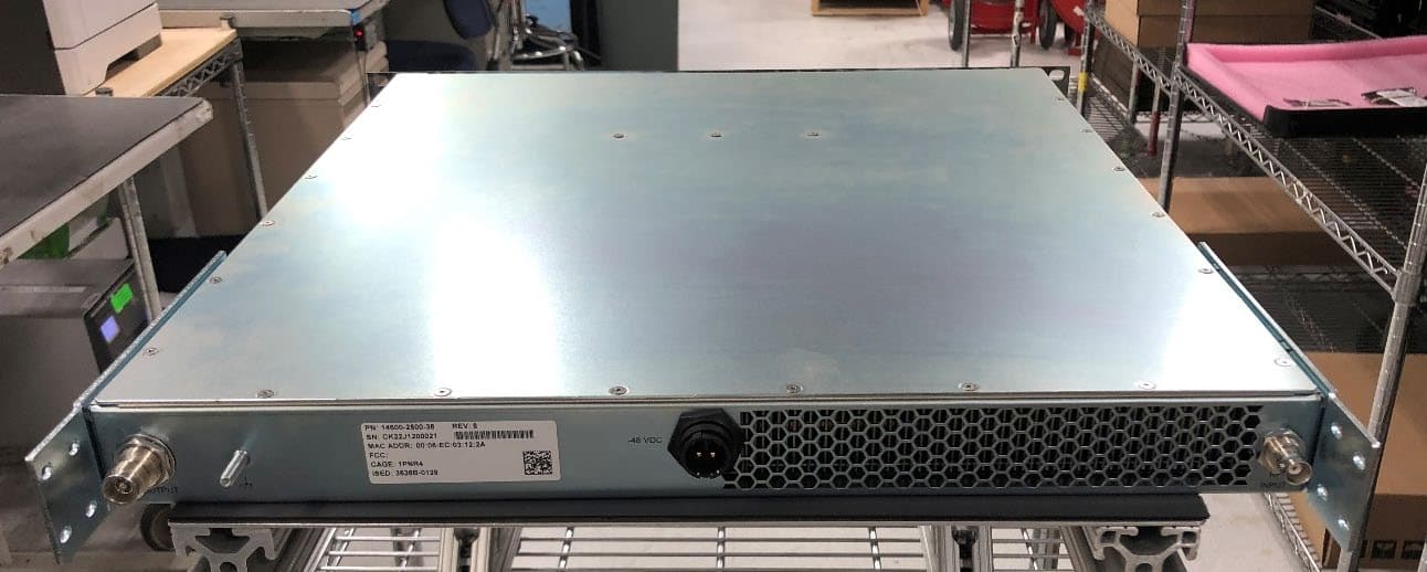
OWDTR-0172-E
Oct 02, 2023Two47, Base Station Transceiver (700 MHz Band)
Equipment Class
TNB - Licensed Non-Broadcast Station Transmitter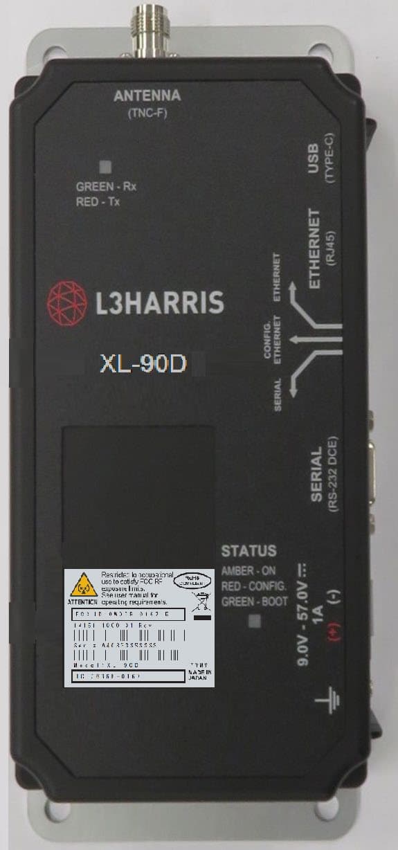
OWDTR-0167-E
Dec 13, 2022XL-90D 7/8/900 MHz Mobile Based Terminal Device
Equipment Class
PCB - PCS Licensed Transmitter
OWDTR-0164-E
Apr 18, 2021XL-400P, Multi-Band Portable Land Mobile Radio
Equipment Class
TNF - Licensed Non-Broadcast Transmitter Held to Face
OWDTR-0162-E
Mar 10, 2021XL-95P, 7/800MHz Portable Land Mobile Radio
Equipment Class
NII - Unlicensed National Information Infrastructure TX