PBJV284-ASubscriber WMU
Vyyo
Click to zoom
Application Details
- Equipment Class
- TNB - Licensed Non-Broadcast Station Transmitter
- Date of Grant
- Nov 20, 2005
- Application Purpose
- Original Equipment
- Date of Application
- Nov 20, 2005
- Equipment Note
- Subscriber WMU
- Frequency Range
- 776.07500000 - 776.92500000
- Company
- Vyyo
- Country
- United States
Documents & Files
Document Text
Text extracted from the exhibit documents filed with the FCC. Open a document above to read the original.
Users Manual
A Vyyo Inc. Technical Document V284-A WIRELESS MODEM UNIT User’s Guide Version 1.1.5 P/N 9090-096 i Vyyö V284-A WMU User’s www.vyyo.com Copyright and Trademark Information: © 2005 Vyyo Inc. All rights reserved. Vyyo Inc. reserves the right to alter the equipment specifications and descriptions in this publication without prior notice. No part of this publication shall be deemed part of any contract or warranty unless specifically incorporated by reference into such contract or warranty. The information contained herein is merely descriptive in nature, and does not constitute a binding offer for the sale of the product described herein. Any use of the Vyyo Inc. logo or trademarks is forbidden without prior written approval from Vyyo Inc. All trademarks mentioned herein are the property of their respective owners. Vyyo Inc.’s trademarks include, but are not limited to, “Vyyo” and “Wireless liberty for all.” ii Vyyö V284-A WMU User’s www.vyyo.com FCC Compliance Statement NOTE: This equipment is authorized under FCC ID No. PBJV284-A to operate in the A Block of the Upper 700 MHz Guard Band pursuant to Part 27 of the FCC’s rules. In addition, this equipment has been tested and found to comply with the limits for a Class B digital device pursuant to Part 15 of the FCC Rules. These limits are designed to provide reasonable protection against harmful interference in a residential installation. This equipment generates, uses and can radiate radio frequency energy and, if not installed and used in accordance with the instructions, may cause harmful interference to radio communications. However, there is no guarantee that interference will not occur in a particular installation. If this equipment does cause harmful interference to radio or television reception, which can be determined by turning the equipment off and on, the user is encouraged to try to correct the interference by one or more of the following measures: • Reorient or relocate the antenna. • Increase the distance between the equipment and receiver. • Connect the equipment into an outlet on a circuit different from that to which the receiver is connected. • Consult the dealer or an experienced radio/TV technician for help. Warning! Changes or modifications to this equipment not expressly approved by Vyyo, Inc. could void the user’s authority to operate the equipment. Warning! This product was tested and shipped with shielded coaxial cable and Category 5 Ethernet cable equipped with a shielded RJ-45 connector. These cables must be used with the unit to ensure compliance. iii Vyyö V284-A WMU User’s www.vyyo.com CONTENTS 1 Overview and Purpose ..................................................... 1 1.1 Purpose of This User’s Guide .......................................... 1 1.2 Target Audience............................................................... 1 1.3 Vyyo ................................................................................. 1 2 Modem Features and Components ................................. 2 2.1 Front Panel Indicators ...................................................... 2 2.2 Rear Panel Connectors.................................................... 4 3 Using the Modem .............................................................. 5 4 Technical Specifications .................................................. 6 5 Problem Troubleshooting ................................................ 8 6 Warranty Information ........................................................ 10 7 FCC Declaration of Conformity........................................ 11 8 Contacting Vyyo................................................................ 12 1 Vyyö V284-A WMU User’s www.vyyo.com 1 OVERVIEW AND PURPOSE Welcome to the User’s Guide for the Vyyo Inc. V284-A Modem. Figure 1-1: The Vyyo V284-A Wireless Modem Unit 1.1 Purpose of This User’s Guide The purpose of this User’s Guide is to provide clear and concise instructions for operating the Vyyo Inc. V284-A modem. 1.2 Target Audience This User’s Guide is intended for users of the V284-A modem. 1.3 Vyyo Vyyo Inc. provides fixed wireless broadband end-to-end telephony and high-speed data connections to business and residential subscribers. Vyyo Inc. technology uses point-to- multipoint architecture to deliver circuit-switched telephony and data over IP to commercial and private customers throughout the world. 2 Vyyö V284-A WMU User’s www.vyyo.com 2 MODEM FEATURES AND COMPONENTS The V284-A modem offers the following features: • Point-to-multipoint broadband wireless Internet access • Superior operations over a wide range of modulation formats and IF bandwidths, including noisy channels • Easy installation • Robust RF performance • Internal radio for UHF bands 2.1 Front Panel Indicators Four Light Emitting Diode (L.E.D.) indicators are located at the front of the modem. The L.E.D.s provide information about the type and status of modem operations, as described in Table 1. Figure 2-1: V284-A WMU Front Panel L.E.D. Indicators 3 Vyyö V284-A WMU User’s www.vyyo.com Table 2-1: L.E.D. Status and Functions L.E.D. Indicator Function POWER • On = Power On • Off = Power Off • Flashing = Fatal Error STATUS • On = Modem is connected to the Internet • Off = Modem is not connected to the Internet RF LINK When Status L.E.D. is Off: • RF On = The downstream link is operational • RF Off = The modem has not yet begun downstream acquisition, the downstream link is idle, or there is a problem with data reception • RF Flashing = Downstream link is being acquired When Status L.E.D. is On: • RF Flashing = Data is transferring in either in the Upstream or Downstream direction LAN& USB • On = The LAN link is operational • Off = The LAN link is not operational • Flashing = Data is transferring to or from the LAN 4 Vyyö V284-A WMU User’s www.vyyo.com 2.2 Rear Panel Connectors There are four connectors located on the rear panel of the V284-A modem. Figure 2-2: V284-A WMU Rear Panel Connectors Connector or Button Func…
Text truncated - open the document above for the full version.
Block Diagram
Vyyo Inc. FCC ID:PBJV284-A Page 1 of 1
Cover Letter(s)
October 16, 2005 American TCB 6731 Whittier Ave. Suite C110 McLean, VA 22101 USA Subject: Request for confidentiality for Wireless Modem Unit, FCC ID:PBJV284-A Dear Gentlemen, In regards the exhibits submitted in support of the application for FCC ID:PBJV284-A, please classify the following as confidential under the provision of 47 CFR 0.459: 1) Schematic diagram, file “Schematics_16544” (1 page). 2) BOM, file “Part_list_16544” (2 pages). 3) Description, file “Schematic_description_16544” (2 pages) The above material contains trade secrets or technical data which Vyyo Inc. deems to be proprietary. Therefore this information would customarily be guarded from competitors and cannot be accessible to the general public. Sincerely, Dr. Mike Ritter V.P. Marketing
Cover Letter(s)
American Telecommunications Certification Body Inc. 6731 Whittier Ave, McLean, VA 22101 October 28, 2005 RE: Vyyo Inc. FCC ID: PBJV284-A After a review of the submitted information, I have a few comments on the above referenced Application. 1) Please provide an internal photograph #3 with all shields removed. 2) Please explain how the 75 to 50 ohm conversions were taken into account in any testing done with a direct attachment to the antenna port (i.e. power, conducted spurious, bandedge etc.). The concern is that many measurements are marginal to limits, and typically the insertion of a minimum-loss pad (75 to 50 ohms) requires a correction of about 5.72 dB. 3) Please explain why the power limit for FCC ID: PBJV284 was use for fixed installation, while the FCC ID: PBJV284-A was used as mobile/control stations. This appears inconsistent as both appear to have a 30 W ERP limitation. 4) Please explain how power output was calibrated in terms of RMS equivalent voltage according to 27.50(c)(4). 5) Users manual should contain antenna installation instructions regarding RF exposure conditions necessary for the installer/user to be in compliance with RF exposure requirements and/or any co- location limitations. Please update. 6) Please define and justify the use of the emissions designators given on the 731. Note that the measured bandwidths appear different than on the 731. Additionally, please clarify which is intended for QPSK and which is intended for QAM. 7) Please provide both current and voltage applied into the several elements of the final radio frequency amplifying device for normal operation over the power range per (2.1033(c)(8)). 8) Please explain compliance to 47 CFR 27.55. 9) The report appears to be missing the information required by 25.53(e). 10) FYI....The AC power conducted emissions appear to have an extension between the LISN and Adapter. Generally every effort should be made to plug the adapter as close to the LISN as possible. Please be careful of this in future applications. Timothy R. Johnson Examining Engineer mailto: [email protected] The items indicated above must be submitted before processing can continue on the above referenced application. Failure to provide the requested information may result in application termination. Correspondence should be considered part of the permanent submission and may be viewed from the Internet after a Grant of Equipment Authorization is issued. Please do not respond to this correspondence using the email reply button. In order for your response to be processed expeditiously, you must submit your documents through the AmericanTCB.com website. Also, please note that partial responses increase processing time and should not be submitted. Any questions about the content of this correspondence should be directed to the sender.
Cover Letter(s)
HERM O N LA BO RA TO RIES November 20, 2005 American TCB 6731 Whittier Ave Suite C110 McLean, VA 22101 Attn: Mr. Timothy Johnson, Examining Engineer RE: your e-mail dated October 28, 2005; Vyyo Ltd. FCC ID: PBJV284-A, ATCB002898 Dear Mr. Johnson, Please find below the answers to your questions. 1) The revised file “Internal_photographs_16544_rev1” with additional photograph #4 of Tuner without shields was uploaded on November 20, 2005 via Internal Photographs folder. 2) The 1.9 dB voltage division correction factor generally represents the worst case for ideal source, internal impedance 75 Ohm and load. In this configuration the difference between measurements at 50 Ohm and 75 Ohm loads will be expressed by the following equation: V@50 Ohm / V@75 Ohm= Vemf(50/(75+50))/ Vemf(75/(75+75))= 0.8 or in logarithmic units 20 log 0.8 = -1.9 dB. For power correction the situation is even better: P@75 Ohm (dBm) = V@75 Ohm (dBuV) - 108.7 dB P@50 Ohm (dBm) = V@50Ohm (dBuV) - 107 dB Assuming the correction factor will be added, we obtain P@50 Ohm (dBm) = V@50 Ohm (dBuV) - 107 dB - 1.9 dB = V@50 Ohm (dBuV) - 108.9 dB or 0.2 dB correction. The similar corrections used in ESA series of spectrum analyzers from Agilent for 50 and 75 Ohm inputs. The 75 Ohm to 50 Ohm direct transaction corresponds to VSWR=1.5 or 0.2 reflection coefficient. The most of spectrum analyzers yields the same VSWR, so generally saying this is still uncertain will it give the result closer to the "true" one or not. Moreover, the VSWR of the EUT output port is not considered at all, which may be much higher than at the spectrum analyzer input. That is why, we used VSWR=1.5 0.2 reflection coefficient for spectrum analyzer and VSWR=2 0.33 reflection coefficient for EUT antenna port in the measurement uncertainty calculations. These parameters fully cover the range of measurements . 3) The device is classified as a mobile one. 4) There is no true RMS detector in the spectrum analyzer we used for the test as well as in the most spectrum analyzers of Agilent. Peak detector was used for testing. The peak detector is calibrated in terms of equivalent RMS voltage/power of the envelope detector . 5) The revised “User_Guide_16544_rev1” with corrected Section 3 “Using the Modem” was uploaded on November 20, 2005 via “Users Manual” folder. 6) The revised ATCB_Form_731_16544_rev1 was uploaded on November 20, 2005 via Application Forms folder. We used the Emission Designator 110KD1W for 16QAM and 112KD1W for QPSK. HERM O N LA BO RA TO RIES 7) Please refer to the document “RF_specifications_16544”, page 2, Table “General”, Power Amplifier: 6 V, 650 mA. 8) The field strength at any location depends on the installation conditions: a) Antenna b) Height above sea level c) Feeder loss. These conditions will be defined by a licensee holder and depend on a licensee bureau. 9) The revised test report VYYRAD_FCC.16544_rev1 with additional section 7.8 and Attachment to setup photos, file “Setup_photos_16544_attachment” were uploaded on November 20, 2005. 10) Thank you for the help. Sincerely, Marina Cherniavsky, certification engineer Hermon Laboratories
External Photos
Vyyo Inc. FCC ID:PBJV284-A Date: October 2005 Page 1 of 7 EXTERNAL PHOTOGRAPHS This document contains 6 photographs Vyyo Inc. FCC ID:PBJV284-A Date: October 2005 Page 2 of 7 Photograph No.1 Top view Vyyo Inc. FCC ID:PBJV284-A Date: October 2005 Page 3 of 7 Photograph No.2 Side view Vyyo Inc. FCC ID:PBJV284-A Date: October 2005 Page 4 of 7 Photograph No.3 General view in standing position Vyyo Inc. FCC ID:PBJV284-A Date: October 2005 Page 5 of 7 Photograph No.4 Rear view Vyyo Inc. FCC ID:PBJV284-A Date: October 2005 Page 6 of 7 Photograph No.5 Antenna connector Vyyo Inc. FCC ID:PBJV284-A Date: October 2005 Page 7 of 7 Photograph No.6 Front view
ID Label/Location Info
Vyyo Inc. FCC ID:PBJV284-A Date: October 2005 Page 1 of 2 LABEL The label shown below is affixed on the rear panel of the V284-A unit. The label material is PVC with a permanent adhesive. Label location on the V284-A rear panel, FCC ID:PBJV284-A Vyyo Inc. FCC ID:PBJV284-A V284-A - Modem. H H / / W W V V e e r r . . : : S S / / W W V V e e r r . . : : M M a a c c A A d d d d r r e e s s s s S S e e r r i i a a l l N N o o . . : : F F C C C C I I D D : : P P B B J J V V 2 2 8 8 4 4 - - A A This device complies with Part 15 of the FCC Rules. Operation is subject to the following two conditions: 1) This device may not cause harmful interference, and 2) This device must accept any interference received, including interference that may cause u undesired operation This Class B digital apparatus complies with Canadian ICES-003. Cet appareil numarique de la classe B est conforme a la norme NMB-003 du Canada. D D C C I I n n p p u u t t : : 1 1 2 2 V V D D C C / / 1 1 . . 2 2 5 5 A A Made in China
Internal Photos
Vyyo Inc. FCC ID:PBJV284-A Date: October 2005 Page 1 of 8 INTERNAL PHOTOGRAPHS, Rev1 This document contains 7 photographs Vyyo Inc. FCC ID:PBJV284-A Date: October 2005 Page 2 of 8 Photograph No.1 Internal view Vyyo Inc. FCC ID:PBJV284-A Date: October 2005 Page 3 of 8 Photograph No.2 Internal view without cover Vyyo Inc. FCC ID:PBJV284-A Date: October 2005 Page 4 of 8 Photograph No.3 RF module Vyyo Inc. FCC ID:PBJV284-A Date: October 2005 Page 5 of 8 Photograph No.4 RF part with shields removed Vyyo Inc. FCC ID:PBJV284-A Date: October 2005 Page 6 of 8 Photograph No.5 Antenna connector Vyyo Inc. FCC ID:PBJV284-A Date: October 2005 Page 7 of 8 Photograph No.6 Close view of the RF part Vyyo Inc. FCC ID:PBJV284-A Date: October 2005 Page 8 of 8 Photograph No.7 Print side of the PCB
Parts List/Tune Up Info
Vyyo Inc. FCC ID: PBJV284-A Date: September 2005 Page 1 of 1 V284-A Tune Up Procedure over the power General: The modem output level is controlled by the WMTS in a periodic ranging procedure. The WMTS set the modem TX level such that it will receive a fix predetermined level. The procedure is based on the DOCSIS procedure. Step 1: Initial ranging: After acquisition of downstream signal, the modem starts to send upstream messages. The modem starts to transmit at the minimum TX level. If this signal was acquired by the WMTS, The WMTS will send an acknowledgment, including a message with a correction of the TX level (to be received at the nominal RX level). The modem is waiting to the acknowledgment. If the modem is not getting an acknowledgment, it increases the TX level by a 6 dB step. This procedure is going on till the modem is getting acknowledgment with the correct TX level, or till it arrives the maximum power. If the modem arrived the maximum power, without getting an acknowledgment, it starts the procedure from the beginning. Step 2: Periodic ranging After the initial ranging, the modem is getting a periodic ranging message from the WMTS. This message includes fine correction of TX level, if needed. The periodic ranging period is typically 3 seconds (can be define through the NMS). Maximum output power: The modem cannot transmit above a pre-defined output level.
Test Report
Hermon Laboratories Ltd. P.O.Box 23, Binyamina 30500, Israel Tel. +972 4628 8001 Fax. +972 4628 8277 E-mail: [email protected] Page 1 of 135 Report ID: VYYRAD_FCC.16544_rev2.doc Date of Issue: November 2005 Electrical TEST REPORT ACCORDING TO: FCC part 27: 2004 FCC part 15: 2005 subpart B FOR: Vyyo Ltd. Wireless modem Model:V284-A This report is in conformity with ISO/ IEC 17025. The A2LA logo endorsement applies only to the test methods and the standards that are listed in the scope of Hermon Laboratories accreditation. The test results relate only to the items tested. This test report shall not be reproduced in any form except in full with the written approval of Hermon Laboratories Ltd. Report ID: VYYRAD_FCC.16544_rev2.doc Date of Issue: November 2005 Project: 16544 Page 2 of 135 Table of contents 1 Applicant information..................................................................................................................................................... 3 2 Equipment under test attributes .................................................................................................................................... 3 3 Manufacturer information .............................................................................................................................................. 3 4 Test details.................................................................................................................................................................... 3 5 Tests summary.............................................................................................................................................................. 4 6 EUT description............................................................................................................................................................. 5 6.1 General information....................................................................................................................................................... 5 6.2 Ports and lines .............................................................................................................................................................. 5 6.3 Support and test equipment .......................................................................................................................................... 5 6.4 Operating frequencies ................................................................................................................................................... 5 6.5 Changes made in the EUT ............................................................................................................................................ 5 6.6 Test configuration.......................................................................................................................................................... 6 6.7 Transmitter characteristics ............................................................................................................................................ 7 7 Transmitter characteristics ............................................................................................................................................ 8 7.1 Peak output power test.................................................................................................................................................. 8 7.2 RF exposure................................................................................................................................................................ 11 7.3 Spurious emissions at RF antenna connector test ...................................................................................................... 13 7.4 Adjacent channel coupled power test.......................................................................................................................... 24 7.5 Radiated spurious emission measurements................................................................................................................ 69 7.6 Frequency stability test................................................................................................................................................ 87 7.7 Occupied bandwidth test ............................................................................................................................................. 91 7.8 Radiated spurious emission measurements in 1559-1610 MHz band ........................................................................ 97 8 Emissions tests according to 47CFR part 15 subpart B requirements ...................................................................... 101 8.1 Conducted emissions ................................................................................................................................................ 101 8.2 Radiated emission measurements ............................................................................................................................ 104 8.3 Antenna power conducted measurements for receiver ............................................................................................. 113 9 APPENDIX A Test equipment and ancillaries used for tests..................................................................................... 118 10 APPENDIX B Measurement uncertainties................................................................................................................. 120 11 APPENDIX C Test facility description ....................................................................................................................... 121 12 APPENDIX D Specification references ..................................................................................................................... 121 13 APPENDIX E Abbreviations and acronyms.......................................................................................................…
Text truncated - open the document above for the full version.
Test Setup Photos
Vyyo Inc. FCC ID:PBJV284-A Date: October 2005 Page 1 of 8 SETUP PHOTOGRAPHS This document contains 7 photographs Vyyo Inc. FCC ID:PBJV284-A Date: October 2005 Page 2 of 8 Photograph No.1 Peak output power, adjacent channel coupled power and spurious emissions at RF antenna connector test setup Vyyo Inc. FCC ID:PBJV284-A Date: October 2005 Page 3 of 8 Photograph No.2 Maximum permissible exposure (MPE) measurement setup Vyyo Inc. FCC ID:PBJV284-A Date: October 2005 Page 4 of 8 Photograph No.3 Setup for spurious emission field strength measurements in 9 kHz to 30 MHz range in the anechoic chamber Vyyo Inc. FCC ID:PBJV284-A Date: October 2005 Page 5 of 8 Photograph No.4 Setup for spurious emission field strength measurements in 30 MHz to 1 GHz range in the anechoic chamber Vyyo Inc. FCC ID:PBJV284-A Date: October 2005 Page 6 of 8 Photograph No.5 Setup for spurious emission field strength measurements above 1 GHz in the anechoic chamber Vyyo Inc. FCC ID:PBJV284-A Date: October 2005 Page 7 of 8 Photograph No.6 Setup for substitution ERP measurements of spurious Vyyo Inc. FCC ID:PBJV284-A Date: October 2005 Page 8 of 8 Photograph No.7 Setup for conducted emission measurements at the mains power port
Test Setup Photos
Vyyo Inc. FCC ID:PBJV284-A Date: November 2005 Page 1 of 3 ATTACHMENT TO SETUP PHOTOGRAPHS This document contains 2 photographs Vyyo Inc. FCC ID:PBJV284-A Date: November 2005 Page 2 of 3 Photograph No.1 Setup for spurious emission field strength measurements in 1559-1610 MHz at the OATS Vyyo Inc. FCC ID:PBJV284-A Date: November 2005 Page 3 of 3 Photograph No.2 Setup for substitution EIRP measurements of spurious
Contact Information
Applicant
Dr. Mike Ritter(VP Marketing)
Technical Contact
Hermon LaboratoriesAlex Usoskin
[email protected]972 4 628-8001
Harakevet Industrial zone · Binyamina · Israel
Non-Technical Contact
Vyyo Ltd.Hila Cohen
[email protected]+972 3976 9999
Test Firm
Hermon Laboratories Ltd.Alexander Usoskin
Technical Specifications
| # | Rule Parts | Frequency Range | Power Output | Emission | Tolerance |
|---|---|---|---|---|---|
| 2 | 27 | 776.075 MHz - 776.925 MHz | 247.00 mW | 112KG1W | 1351 Hz |
Other Applications from Vyyo

PBJV284-PLUS-A
Apr 10, 2006Subscriber WMU
Equipment Class
TNB - Licensed Non-Broadcast Station Transmitter
PBJV3000-C
Mar 02, 2006Base Station Transmitter
Equipment Class
TNB - Licensed Non-Broadcast Station Transmitter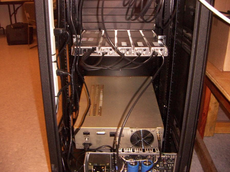
PBJV3000-A
Jan 29, 2006Base Station Transmitter
Equipment Class
TNB - Licensed Non-Broadcast Station Transmitter
PBJV284-PLUS-C
Dec 20, 2005Subscriber WMU
Equipment Class
TNB - Licensed Non-Broadcast Station Transmitter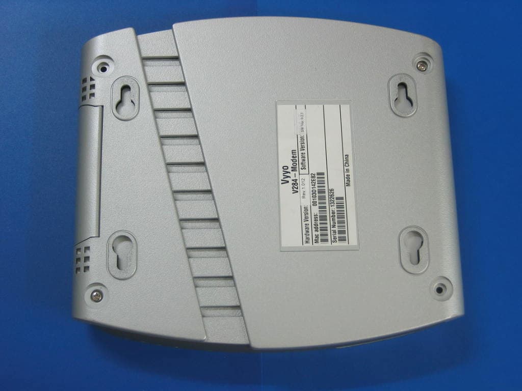
PBJV284
Nov 14, 2005Subscriber WMU
Equipment Class
TNB - Licensed Non-Broadcast Station Transmitter