PD97260NAIntel 7260M2NA
Intel Corporation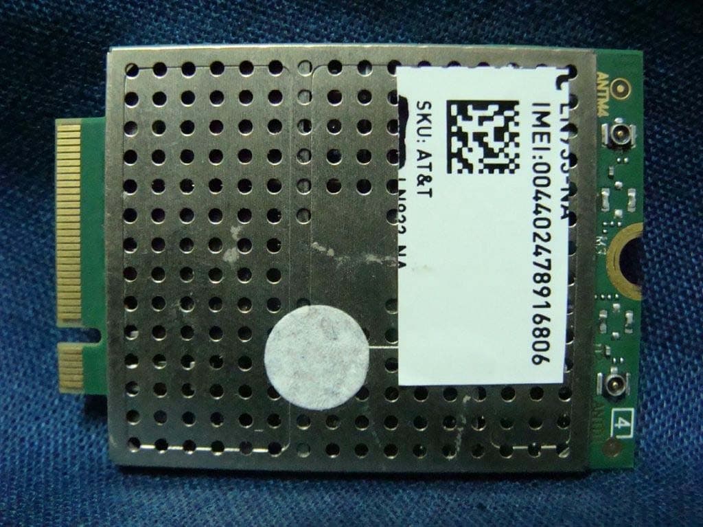
Click to zoom
Application Details
- Equipment Class
- PCB - PCS Licensed Transmitter
- Date of Grant
- Dec 18, 2014
- Application Purpose
- Original Equipment
- Date of Application
- Dec 17, 2014
- Equipment Note
- Intel 7260M2NA
- Frequency Range
- 1720.00000000 - 1745.00000000
- Company
- Intel Corporation
- Country
- France
Documents & Files
Document Text
Text extracted from the exhibit documents filed with the FCC. Open a document above to read the original.
Users Manual
Document Number: N/A Intel 7260M2NA User Guide Revision 1.0, August‐2014 Revision History Rev. 1.0, September‐2012 2/60 Hardware User Guide, Document Number: N/A Revision History Revision Number Description Revision Date 1.0 Initial version of the document 17‐Dec‐2012 Revision History Rev. 1.0, September‐2012 3/60 Hardware User Guide, Document Number: N/A Contents 1 Introduction ................................................................................ 9 2 Software Framework ............................................................. 12 2.1 Driver Installation................................................................... 12 2.1.1 General Considerations ........................................................ 12 2.1.2 Intel High Speed Modem Driver (ecm200) .................. 14 2.1.2.1 Client offset configuration. ................................................. 19 2.1.2.2 Static IP Address Configuration ........................................ 21 2.1.3 Comneon High Speed Modem Driver .............................. 25 2.1.4 Flash USB driver and FTDI Driver .................................... 28 2.1.5 Prolific Serial to USB Driver ................................................ 29 2.2 LTE debug UART configuration .......................................... 30 2.3 System Trace Box .................................................................. 33 Revision History Rev. 1.0, September‐2012 4/60 Hardware User Guide, Document Number: N/A 2.3.1 Setup and Configuration ...................................................... 33 2.3.1.1 Entering AT Commands ....................................................... 33 2.3.1.2 Board Configuration and required AT Commands ..... 34 2.3.2 Connecting the UE .................................................................. 35 2.4 AT Commands Examples ..................................................... 37 3 Test Cases ................................................................................. 42 3.1 Protocol Test (CMW500) ...................................................... 42 3.1.1 CWM 500 Firmware ............................................................... 42 3.1.2 Test Scenario ........................................................................... 44 3.1.3 AT Commands .......................................................................... 45 3.1.4 The Data Application Unit .................................................... 45 4 Regulatory Notice ................................................................... 50 5 Abbreviations / Terminology .............................................. 51 Revision History Rev. 1.0, September‐2012 5/60 Hardware User Guide, Document Number: N/A Appendix A ................................................... Definitions/Explanations ....................................................................................................... 53 Figures Figure 1. Location of the Prolific serial to USB driver, the Flash USB driver and the FTDI diver within the flash tool folder. ................................................................. 13 Figure 2. Use the already installed driver. ................... 15 Figure 3. Install the driver again. .................................... 16 Figure 4. The network modem and four COM ports are now appearing at the device manager. ............ 16 Figure 5. Open the network connections dialog. Win XP : Start:Settings:NetworkConnectios. A new network device did pop up. It is not yet connected. .................................................................................................. 17 Revision History Rev. 1.0, September‐2012 6/60 Hardware User Guide, Document Number: N/A Figure 6. On Win7: Select “Start:Control Panel:Network and Sharing Center” followed by “Change adapter settings”. ............................................ 18 Figure 7. Open the properties dialog of the new network device (right click). .......................................... 18 Figure 8. Select the configuration dialog. ..................... 19 Figure 9. Set the client offset to 1 and press “OK”. . 20 Figure 10. Press “OK” to save these settings. Otherwise these settings get lost. .............................. 20 Figure 11. Open the Internet Protocol TCP/IP settings. ................................................................................. 23 Figure 12. Set the static Network IP and press OK. . 24 Figure 13. To close the properties dialog and save the settings press “OK”. .................................................. 25 Revision History Rev. 1.0, September‐2012 7/60 Hardware User Guide, Document Number: N/A Figure 14. Congratulations. Your ecm200 driver and its IP connection are now properly configured. ..... 25 Figure 15. Use the already installed driver. ................. 26 Figure 16. Install the driver. .............................................. 27 Figure 17. Comneon suspend and six COM ports are now appearing at the device manager. .................... 28 Figure 18. USIF1 Device Manager Prolific USB-to- Serial COM Port .................................................................. 30 Figure 19. Putty configuration. ......................................... 32 Figure 20. CMW 500 .............................................................. 42 Tables Table 1. Terminal Port Settings ........................................ 31 Table 2. AT Commands trace box support. ............. Error! Bookmark not defined. Revision History Rev. 1.0, September‐2012 8/60 Hardware User Guide, Document Number: N/A Table 3. Terminal Port Settings ........................................ 38 Table 4. AT Commands to check ARM software version ................................................................................... 38 Table 5. AT Commands to Register on the Network 38 Table 6. AT Commands for an Incoming Call .............. 38 Table 7. AT Commands for an Outgoing Call .............. 39 Table 8. AT Commands for SMS Management ............ 39 Revision Hist…
Text truncated - open the document above for the full version.
Attestation Statements
Intel Mobile Communications 100 Center Point Circle, Suite 200 Columbia, South Carolina 29210 USA Nov 21, 2014 Software Security Attestation FCC ID: PD97260NA Model: Intel 7260M2NA To Whom It May Concern, This letter is to confirm there are no user controls or software provided that will allow critical radio parameters to be altered or changed to operate the device outside the authorized conditions or to allow operation outside the USA. We don't provide any controls or software to allow operation outside the USA for devices sold in the USA. Sincerely, Steven C. Hackett Product Regulations Engineer Wireless Platforms R&D TEL: 803-216-2344 CELL: 803-315-6704 [email protected]
Cover Letter(s)
100 Center Point Circle Columbia, SC 29210 Authority to Act as Agent November 20, 2014 American Certification Body, Inc. 6731 Whittier Avenue Suite C110 McLean, VA 22101 To Whom It May Concern: Quietek is authorized to act on our behalf, until otherwise notified, for applications to American Certification Body, Inc. (ACB). Intel retains the rights to communicate or obtain information directly from ACB or Quietek at our discretion at any time regarding applications made on our behalf. We certify that we are not subject to denial of federal benefits, that includes FCC benefits, pursuant to Section 5301 of the Anti-Drug Abuse Act of 1988, 21 U.S.C. 862. Further, no party, as defined in 47 CFR 1.2002 (b), to the application is subject to denial of federal benefits, that includes FCC benefits. Thank you, Agency Agreement Expiration Date: November 21, 2015 By: Steven C. Hackett (Signature 1 ) (Print name) Title: Wireless Regulations Engineer On behalf of: Intel Mobile Communications (Company Name) Telephone: 803-216-2344
Cover Letter(s)
100 Center Point Circle Columbia, SC 29210 November 21, 2014 Subject: Confidentiality Request for FCC ID: PD97260NA Pursuant to FCC 47 CRF 0.457(d) and 0.459 the applicant requests that a part of the subject FCC application be held confidential. Type of Confidentiality Requested Exhibit Short Term Permanent Block Diagrams Short Term External Photos Short Term Permanent Internal Photos Short Term Permanent Operation Description/Antenna Specification Short Term Permanent Operation Description/HW Theory of Operation Short Term Permanent Bill of Materials List Short Term Permanent Schematics Short Term Permanent Bill of Materials Short Term Permanent Tune-Up Attestation Short Term Test Setup Photos Short Term Permanent User’s Manual Intel Corporation has spent substantial effort in developing this product and it is one of the first of its kind in industry. Having the subject information easily available to "competition" would negate the advantage they have achieved by developing this product. Not protecting the details of the design will result in financial hardship. Permanent Confidentiality: The applicant requests the exhibits listed above as permanently confidential be permanently withheld from public review due to materials that contain trade secrets and proprietary information not customarily released to the public. Short-Term Confidentiality: The applicant requests the exhibits selected above as short term confidential be withheld from public view for a period of 180 days from the date of the Grant of Equipment Authorization and prior to marketing. This is to avoid premature release of sensitive information prior to marketing or release of the product to the public. Applicant is also aware that they are responsible to notify ATCB in the event information regarding the product or the product is made available to the public. ATCB will then release the documents listed above for public disclosure pursuant to FCC Public Notice DA 04- 1705. Sincerely, Steven C. Hackett By: __________________________ ________________________ (Signature/Title 1 ) (Print Name)
Cover Letter(s)
Intel Corporation 100 Center Point Circle Columbia, SC 29210 Modular Approval Requirements Attestation FCC ID: PD97260NA IC: 1000M-7260NA (Model 7260M2NA) Modular Approval is being requested for this device under the ID’s listed above. This device is a self contained, physically delineated, component for which compliance was demonstrated independent of any host operating conditions and complies with all eight requirements of FCC Part 15.212(a)(1) and IC RSS-GEN, 3.2.2. The details of these requirements and the manner in which the devices meet them are summarized below. The module must have its own RF shielding. The module contains a metal shield which covers all RF components and circuitry; this shield is located on the top side of the board located next to the antenna connectors. All modulation and data input(s) are buffered. Data to the modulation circuit is buffered on the module; please refer to the “theory of operation” document filed with this application for full description. The module has its own power supply regulation and local reference oscillator. The module contains its own power supply regulation and the rf reference oscillator is contained within the module. Please refer to the schematics and “theory of operation” documents filed with this application for full description. The modular transmitter must comply with the antenna requirements of Section 15.203 and 15.204(c). The certification submission contains a detailed description of all antennas that will be used with the module. The module connects to its antenna via using an UFL type connector. This antenna connector is a non-standard connector. The antenna tested was a PIFA type and the data sheet is included in the application. The modular transmitter must be tested in a stand-alone configuration, i.e., the module must not be inside another device during testing. Test data contained in this application is for the device tested as a stand-alone device connected externally to a PC. See test set-up photographs filed with this application. For the FCC, the modular transmitter must be labeled with its own FCC ID number, and, if the FCC ID is not visible when the module is installed inside another device, then the outside Intel Corporation 100 Center Point Circle Columbia, SC 29210 of the device into which the module is installed must also display a label referring to the enclosed module. This exterior label can use wording such as the following: “Contains Transmitter Module FCC ID: XYZMODEL1” or “Contains FCC ID: XYZMODEL1.” For Industry Canada, the module meets certification labeling requirements for Category I Equipment. The module is appropriately labeled (refer to the label and label location drawings contained within this application). Information to the integrator of this device regarding the labeling requirements for the host system is contained in the instructions provided with the module. The modular transmitter must comply with any applicable RF exposure requirements. The module meets the requirements for a mobile/portable device that may be used at separation distances of more than 8mm from the human body. Refer to the RF Exposure test report submitted with this application. Sincerely, Steven C. Hackett Product Regulations Engineer [email protected]
External Photos
Report No.: 1490343R-HPUSP11V00 Page : 1 of 4 Attachment 2 : EUT Detailed Photographs (1) EUT Photo (2) EUT Photo Report No.: 1490343R-HPUSP11V00 Page : 2 of 4 (3) EUT Photo (4) EUT Photo
ID Label/Location Info
Intel Mobile Communications 100 Center Point Circle, Suite 200 Columbia, South Carolina 29210 USA Tel : 803-216-2344 IC Label The IC Label will be placed on the equipment as shown in the photograph below.
Internal Photos
Report No.: 1490343R-HPCAP33V00 Page : 1 of 4 Attachment 2 : EUT Detailed Photographs (1) EUT Photo (2) EUT Photo Report No.: 1490343R-HPCAP33V00 Page : 2 of 4 (3) EUT Photo (4) EUT Photo
RF Exposure Info
Report No. 1490343R-RF-US-RFEXP Page: 1 of 5 RF Exposure Evaluation declaration Product Name : Intel 7260M2NA Model No. : 7260M2NA FCC ID : PD97260NA Applicant : Intel Mobile Communications Address : 100 Center Point Circle, Suite 200 Columbia, South Carolina 29210 USA Date of Receipt : Sep. 12, 2014 Date of Declaration : Nov. 21, 2014 Report No. : 1490343R-RF-US-RFEXP The test results relate only to the samples tested. The test results shown in the test report are traceable to the national/international standard through the calibration of the equipment and evaluated measurement uncertainty herein. This report must not be used to claim product endorsement by TAF or any agency of the government. The test report shall not be reproduced without the written approval of QuieTek Corporation. Report No. 1490343R-RF-US-RFEXP Page: 2 of 5 1. GENERAL INFORMATION 1.1. EUT Description Product Name Intel 7260M2NA Model No. 7260M2NA Trade Name Intel IMEI No. 004402-xx-xxxxxx-x FCC ID PD97260NA GSM850: 824.2 ~ 848.8 MHz GSM1900: 1850.2~ 1909.8MHz WCDMA Band 2: 1852.4 ~ 1907.6 MHz WCDMA Band 4: 1712.4~ 1752.6 MHz WCDMA Band 5: 826.4~ 846.6 MHz LTE Band 2: 1850~1910MHz LTE Band 4: 1710~1755MHz LTE Band 5: 824~849MHz TX Frequency LTE Band 17: 704~716MHz GSM850: 869.2 ~ 893.8 MHz GSM1900: 1930.2 ~ 1989.8 MHz WCDMA Band 2: 1932.4 ~ 1987.6 MHz WCDMA Band 4: 2112.4 ~ 2152.6 MHz WCDMA Band 5: 871.4 ~ 891.6 MHz LTE Band 2: 1930~1990MHz LTE Band 4: 2110~2155MHz LTE Band 5: 869~894MHz Rx Frequency LTE Band 17: 734~746MHz HW Version PR3.1 SW Version 1433 Antenna Type Dipole 1.2. Antenna List : No. Manufacturer Part No. Peak Gain 1 Pulse SPDA24700/2700 2dBi Report No. 1490343R-RF-US-RFEXP Page: 3 of 5 2. RF Exposure Evaluation 2.1. Limits According to FCC 1.1310: The criteria listed in the following table shall be used to evaluate the environment impact of human exposure to radio frequency (RF) radiation as specified in 1.1307(b). LIMITS FOR MAXIMUM PERMISSIBLE EXPOSURE (MPE) Frequency Range (MHz) Electric Field Strength (V/m) Magnetic Field Strength (A/m) Power Density (mW/cm 2 ) Average Time (Minutes) (A) Limits for Occupational/ Control Exposures 300-1500 -- -- F/300 6 1500-100,000 -- -- 5 6 (B) Limits for General Population/ Uncontrolled Exposures 300-1500 -- -- F/1500 30 1500-100,000 -- -- 1 30 F= Frequency in MHz Friis Formula Friis transmission formula: Pd = (Pout*G)/(4*Pi*R 2 ) Where Pd = power density in mW/cm 2 Pout = output power to antenna in mW G = gain of antenna in linear scale Pi = 3.1416 R = distance between observation point and center of the radiator in cm Pd is the limit of MPE, 1 mW/cm 2 . If we know the maximum gain of the antenna and the total power input to the antenna, through the calculation, we will know the distance r where the MPE limit is reached. 2.2. Test Procedure Software provided by client enabled the EUT to transmit and receive data at lowest, middle and highest channel individually. The temperature and related humidity: 21°Cand 60% RH. Report No. 1490343R-RF-US-RFEXP Page: 4 of 5 2.3. Test Result of RF Exposure Evaluation Product : Intel 7260M2NA Test Item : RF Exposure Evaluation Test Site : N/A GPRS 850 Peak Gain: 2dBi Frequency Conducted Peak Power (dBm) Maximum ERP (W) Maximum ERP Limit(W) Duty Cycle (%) Conducted Average Power (dBm) Output Power to Antenna (mW) Power Density at R = 20 cm (mW/cm 2 ) Limit (mW/cm 2 ) Pass/Fail 848.8 32.07 1.56 7 12.5 23.04 201.3 0.0635 0.57 Pass 836.4 31.78 1.46 7 25 25.76 376.7 0.1188 0.56 Pass 836.4 31.29 1.30 7 37.5 27.03 504.7 0.1591 0.56 Pass 836.4 30.58 1.10 7 50 27.57 571.4 0.1802 0.56 Pass EGPRS 850 Peak Gain: 2dBi Frequency Conducted Peak Power (dBm) Maximum ERP/EIRP (W) Maximum ERP/EIRP Limit(W) Duty Cycle (%) Conducted Average Power (dBm) Output Power to Antenna (mW) Power Density at R = 20 cm (mW/cm 2 ) Limit (mW/cm 2 ) Pass/Fail 824.2 27.54 0.55 7 12.5 18.51 70.9 0.0224 0.55 Pass 824.2 27.48 0.54 7 25 21.46 139.9 0.0441 0.55 Pass 824.2 26.85 0.47 7 37.5 22.59 181.6 0.0572 0.55 Pass 824.2 25.74 0.36 7 50 22.73 187.5 0.00591 0.55 Pass GPRS 1900 Peak Gain: 2dBi Frequency Conducted Peak Power (dBm) Maximum EIRP (W) Maximum EIRP Limit(W) Duty Cycle (%) Conducted Average Power (dBm) Output Power to Antenna (mW) Power Density at R = 20 cm (mW/cm 2 ) Limit (mW/cm 2 ) Pass/Fail 1850.2 29.84 1.53 2 12.5 20.81 120.5 0.0380 1 Pass 1850.2 29.83 1.52 2 25 23.81 240.4 0.0758 1 Pass 1850.2 29.27 1.34 2 37.5 25.01 317.0 0.0999 1 Pass 1850.2 28.18 1.04 2 50 25.17 328.8 0.1037 1 Pass Report No. 1490343R-RF-US-RFEXP Page: 5 of 5 EGPRS 1900 Peak Gain: 2dBi Frequency Conducted Peak Power (dBm) Maximum EIRP (W) Maximum EIRP Limit(W) Duty Cycle (%) Conducted Average Power (dBm) Output Power to Antenna (mW) Power Density at R = 20 cm (mW/cm 2 ) Limit (mW/cm 2 ) Pass/Fail 1909.8 26.67 0.74 2 12.5 17.64 58.1 0.0183 1 Pass 1909.8 26.76 0.75 2 25 20.74 118.6 0.0374 1 Pass 1909.8 25.99 0.63 2 37.5 21.73 148.9 0.0470 1 Pass 1909.8 24.75 0.47 2 50 21.74 149.3 0.0471 1 Pass WCDMA Peak Gain: 2dBi Band Frequency Conducted Peak Power (dBm) Maximum ERP/EIRP (W) Maximum ERP/EIRP Limit (W) Duty Cycle (%) Conducted Average Power (dBm) Output Power to Antenna (mW) Power Density at R = 20 cm (mW/cm 2 ) Limit (mW/cm 2 ) Pass/Fail II 1852.4 24.66 0.46 2 100 24.66 292.4 0.0922 1 Pass IV 1712.4 24.54 0.45 1 100 24.54 284.4 0.0897 1 Pass V 826.4 23.88 0.24 7 100 23.88 244.3 0.0770 0.55 Pass LTE Peak Gain: 2dBi Band Frequency Conducted Peak Power (dBm) Maximum ERP/EIRP (W) Maximum ERP/EIRP Limit (W) Duty Cycle (%) Conducted Average Power (dBm) Output Power to Antenna (mW) Power Density at R = 20 cm (mW/cm 2 ) Limit (mW/cm 2 ) Pass/Fail II 1855 23.21 0.33 2 100 23.21 209.4 0.0660 1 Pass IV 1750 23.09 0.32 1 100 23.09 203.7 0.0642 1 Pass V 824.7 22.85 0.19 7 100 22.85 192.8 0.0608 0.55 Pass XVII 709 22.82 0.18 3 100 22.82 191.4 0.0604 0.47 Pass Note: The conducted output power is refer to report No.: 1490343R-HPUSP11V00 & 1490343R-HPUSP45V00 from the QuieTek.
Test Report
Report No.:1490343R-HPUSP11V00 Page: 1 of 77 FCC Test Report (Part 22&24&27) Product Name : Intel 7260M2NA Model No : 7260M2NA FCC ID : PD97260NA Applicant : Intel Mobile Communications Address : 100 Center Point Circle, Suite 200 Columbia, South Carolina 29210 USA Date of Receipt:2014/09/12 Issued Date :2014/11/03 Report No. :1490343R-HPUSP11V00 Report Version:V1.0 The test results relate only to the samples tested. The test results shown in the test report are traceable to the national/international standard through the calibration of the equipment and evaluated measurement uncertainty herein. This report must not be used to claim product endorsement by TAF or any agency of the government. The test report shall not be reproduced without the written approval of QuieTek Corporation. Report No.:1490343R-HPUSP11V00 Page: 2 of 77 Test Report Issued Date : 2014/11/03 Report No.: 1490343R-HPUSP11V00 Product Name : Intel 7260M2NA Applicant : Intel Mobile Communications Address : 100 Center Point Circle, Suite 200 Columbia, South Carolina 29210 USA Manufacturer : Intel Mobile Communications Trade Name : Intel Model No. : 7260M2NA EUT Rated Voltage : DC 3.3V EUT Test Voltage DC 3.3V Measurement Standard : FCC CFR Title 47 Part 2 22 24 27 Measurement Reference : TIA/EIA 603-C Test Result : Complied Documented By : (Adm. Specialist / Anny Chou) Tested By : (Senior Engineer / Vorana Chen) Approved By : (Director /Vincent Lin) Report No.:1490343R-HPUSP11V00 Page: 3 of 77 TABLE OF CONTENTS Description Page 1. GENERAL INFORMATION ............................................................................................ 4 1.1. EUT Description ........................................................................................................... 4 1.2. Antenna List.................................................................................................................. 4 1.3. Operational Description............................................................................................... 5 1.4. Configuration of tested System .................................................................................. 6 1.5. EUT Setup Procedures ................................................................................................ 6 1.6. Test Facility ...................................................................................................................7 1.7. Type of Emission ..........................................................................................................8 1.8. Voltages and DC currents ............................................................................................ 8 2. Technical Test ...............................................................................................................9 2.1. Summary of test result ................................................................................................ 9 2.2. List of test Equipment................................................................................................ 10 2.3. Measurement Uncertainty.......................................................................................... 10 3. Conducted Output Power Measurment .................................................................... 11 3.1. Test Specification ....................................................................................................... 11 3.2. Test Setup ................................................................................................................... 11 3.3. Limits ........................................................................................................................... 11 3.4. Test Procedure ........................................................................................................... 11 3.5. Test Result of Maximum Power Output.................................................................... 12 4. Occupied Bandwidth.................................................................................................. 13 4.1. Test Specification ....................................................................................................... 13 4.2. Test Setup ................................................................................................................... 13 4.3. Test Procedure ........................................................................................................... 13 4.4. Test Result of Occupied Bandwidth ......................................................................... 14 5. Spurious Emission At Antenna Terminals (+/-1MHz) .............................................. 29 5.1. Test Specification ....................................................................................................... 29 5.2. Setup ........................................................................................................................... 29 5.3. Limits ........................................................................................................................... 29 5.4. Test Procedure ........................................................................................................... 29 5.5. Test Result of Spurious Emission At Antenna Terminals (+/-1MHz)...................... 30 6. Spurious Emission ..................................................................................................... 37 6.1. Test Specification ....................................................................................................... 37 6.2. Test Setup ................................................................................................................... 37 6.3. Limits ........................................................................................................................... 38 6.4. Test Procedure ........................................................................................................... 38 6.5. Test Result of Spurious Emission …
Text truncated - open the document above for the full version.
Test Report
Report No.:1490343R-HPUSP11V00 Page: 46 of 77 Report No.:1490343R-HPUSP11V00 Page: 47 of 77 Report No.:1490343R-HPUSP11V00 Page: 48 of 77 Product Intel 7260M2NA Test Mode Spurious Emission (Conducted) Date of Test 2014/09/22 Test Site CTR Test Condition PCS 1900 EGPRS Test Range 30MHz~20GHz PCS 1900 EGPRS High-Channel 810 Frequency (MHz) Reading Level (dBm) Path Loss (dB) Emission Level (dBm) Limit (dBm) 3819.6 -46.976 1.1 -45.876 -13 5729.4 -63.933 1.23 -62.703 -13 7639.2 -64.546 1.59 -62.956 -13 9549 -65.187 1.89 -63.297 -13 11458.8 -66.657 2.07 -64.587 -13 13368.6 -64.983 2.26 -62.723 -13 15278.4 -59.957 2.64 -57.317 -13 17188.2 -59.778 3.5 -56.278 -13 19098 -59.012 3.7 -55.312 -13 Report No.:1490343R-HPUSP11V00 Page: 49 of 77 Report No.:1490343R-HPUSP11V00 Page: 50 of 77 Report No.:1490343R-HPUSP11V00 Page: 51 of 77 Product Intel 7260M2NA Test Mode Spurious Emission (Conducted) Date of Test 2014/09/22 Test Site CTR Test Condition WCDMA BAND 2 Test Range 30MHz~20GHz WCDMA BAND 2 Mid-Channel 9400 Frequency (MHz) Reading Level (dBm) Path Loss (dB) Emission Level (dBm) Limit (dBm) 3708 -54.242 1.1 -53.142 -13 5557.2 -64.013 1.23 -62.783 -13 7409.6 -65.668 1.59 -64.078 -13 9262 -65.918 1.89 -64.028 -13 11114.4 -66.381 2.07 -64.311 -13 12966.8 -64.998 2.26 -62.738 -13 14819.2 -60.079 2.64 -57.439 -13 16671.6 -59.279 3.5 -55.779 -13 18524 -57.988 3.7 -54.288 -13 Report No.:1490343R-HPUSP11V00 Page: 52 of 77 Report No.:1490343R-HPUSP11V00 Page: 53 of 77 Report No.:1490343R-HPUSP11V00 Page: 54 of 77 Product Intel 7260M2NA Test Mode Spurious Emission (Conducted) Date of Test 2014/09/22 Test Site CTR Test Condition WCDMA BAND 4 Test Range 30MHz~20GHz WCDMA BAND 4 Low-Channel 1312 Frequency (MHz) Reading Level (dBm) Path Loss (dB) Emission Level (dBm) Limit (dBm) 3424.8 -57.188 1.1 -56.088 -13 5137.2 -55.690 1.23 -54.460 -13 6849.6 -64.060 1.59 -62.470 -13 8562 -65.474 1.89 -63.584 -13 10274.4 -65.945 2.07 -63.875 -13 11986.8 -65.532 2.26 -63.272 -13 13699.2 -62.949 2.64 -60.309 -13 15411.6 -60.070 3.5 -56.570 -13 17124 -59.582 3.7 -55.882 -13 Report No.:1490343R-HPUSP11V00 Page: 55 of 77 Report No.:1490343R-HPUSP11V00 Page: 56 of 77 Report No.:1490343R-HPUSP11V00 Page: 57 of 77 Product Intel 7260M2NA Test Mode Spurious Emission (Conducted) Date of Test 2014/09/22 Test Site CTR Test Condition WCDMA BAND 5 Test Range 30MHz~10GHz WCDMA BAND 5 Low-Channel 4132 Frequency (MHz) Reading Level (dBm) Path Loss (dB) Emission Level (dBm) Limit (dBm) 1651 -60.487 0.58 -59.907 -13 2479.2 -62.412 0.7 -61.712 -13 3305.6 -65.247 1.01 -64.237 -13 4132 -65.396 1.18 -64.216 -13 4958.4 -63.744 1.23 -62.514 -13 5784.8 -61.810 1.45 -60.360 -13 6611.2 -62.703 1.56 -61.143 -13 7437.6 -65.747 1.59 -64.157 -13 8264 -65.549 1.82 -63.729 -13 Report No.:1490343R-HPUSP11V00 Page: 58 of 77 Report No.:1490343R-HPUSP11V00 Page: 59 of 77 Report No.:1490343R-HPUSP11V00 Page: 60 of 77 Product Intel 7260M2NA Test Mode Spurious Emission (Radiated) Date of Test 2014/10/10 Test Site Site3 Test Condition Channel 251 (GSM 850 GPRS) Test Range 9kHz ~10GHz Frequency Reading Level Signal Generator Level Cable Loss Antenna Gain EIRP Value Limit (GHz) (dBm) (dBm) (dB) (dBi) (dBm) (dBm) Horizontal Emissions 1698.000 -49.476 -52.212 1.630 9.800 -44.042 -13 2545.000 -38.485 -39.314 2.100 10.600 -30.814 -13 3395.000 -54.914 -56.399 2.350 12.300 -46.449 -13 4244.000 -55.406 -53.690 2.700 12.600 -43.790 -13 5093.000 -53.943 -49.379 2.830 12.700 -39.509 -13 5942.000 -52.196 -47.987 3.200 13.000 -38.187 -13 Vertical Emissions 1698.000 -54.225 -56.539 1.630 9.800 -48.369 -13 2545.000 -40.455 -40.448 2.100 10.600 -31.948 -13 3395.000 -55.312 -55.697 2.350 12.300 -45.747 -13 4244.000 -57.026 -54.162 2.700 12.600 -44.262 -13 5093.000 -54.803 -49.959 2.830 12.700 -40.089 -13 5942.000 -53.000 -48.732 3.200 13.000 -38.932 -13 Note: 1. Receiver setting (Peak Detector) : RBW:1MHz; VBW:3MHz 2. EIRP Value = Signal Generator Level + Antenna Gain - Cable Loss 3. Spurious emissions past 6 GHz are not shown, due to the magnitude of spurious emissions attenuated more than 20 dB below the limit. Report No.:1490343R-HPUSP11V00 Page: 61 of 77 Product Intel 7260M2NA Test Mode Spurious Emission (Radiated) Date of Test 2014/10/10 Test Site Site3 Test Condition Channel 128 (GSM 850 EGPRS) Test Range 9kHz ~10GHz Frequency Reading Level Signal…
Text truncated - open the document above for the full version.
Contact Information
Applicant
Benjamin Lavenant(Regulatory Engineer)
Technical Contact
QuieTek Corp.Maggie Chen
[email protected]886286013788
No. 5-22, Rueishu Keng, Linkou Dist. · New Taipei City · Taiwan
Test Firm
DEKRA Testing and Certification Co., Ltd.Sky Hsu
Technical Specifications
| # | Rule Parts | Frequency Range | Power Output | Emission | Tolerance |
|---|---|---|---|---|---|
| 43 | 27 | 1.72 GHz - 1.75 GHz | 243.00 mW | 18M8W7D | 0.008 ppm |
Other Applications from Intel Corporation
PD9BE201D2P
Aug 20, 2024Intel BE201D2WP
Equipment Class
NII - Unlicensed National Information Infrastructure TXPD9AX411NG
Jul 02, 2024Intel WiFi 6E AX411
Equipment Class
6CD - 15E 6 GHz Low Power Dual ClientPD9AX211D2H
Jan 28, 2024Intel Wi-Fi 6E AX211
Equipment Class
DSS - Part 15 Spread Spectrum Transmitter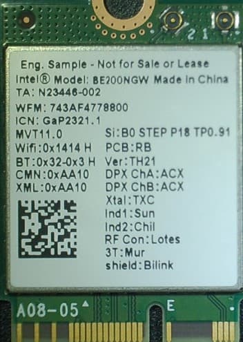
PD9BE200NG
Sep 13, 2023Intel BE200
Equipment Class
6CD - 15E 6 GHz Low Power Dual Client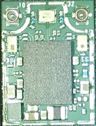
PD9BE200D2
Sep 13, 2023Intel BE200
Equipment Class
6CD - 15E 6 GHz Low Power Dual Client