PD97262W2WWAN Module Adapter Card
Intel Corporation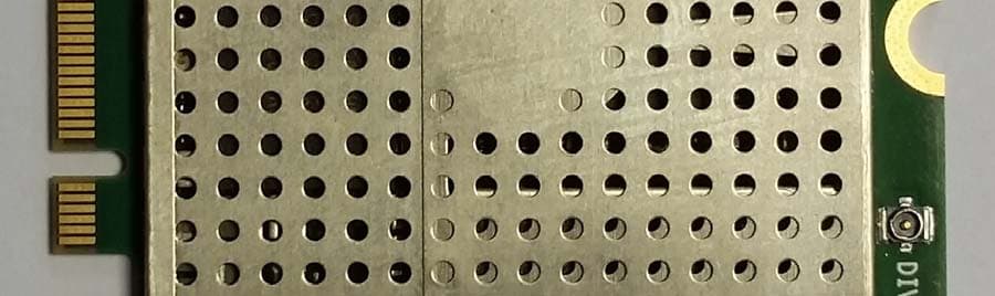
Click to zoom
Application Details
- Equipment Class
- PCB - PCS Licensed Transmitter
- Date of Grant
- Jul 30, 2015
- Application Purpose
- Original Equipment
- Date of Application
- Jul 29, 2015
- Equipment Note
- WWAN Module Adapter Card
- Frequency Range
- 2310.00000000 - 2310.00000000
- Company
- Intel Corporation
- Country
- France
Documents & Files
Document Text
Text extracted from the exhibit documents filed with the FCC. Open a document above to read the original.
Users Manual
Document Number: N/A Intel Model 7260M2NA and 7262M2WW User Guide Revision 1.2, Feb 2015 Revision History Rev. 1.2, Feb. 2015 2/44 Hardware User Guide, Document Number: N/A Revision History Revision Number Description Revision Date 1.0 Initial version of the document 17‐Dec‐2012 1.1 Revise to add model 7260M2NA Nov 2014 1,2 Revise to add model 7262M2WW Feb 2015 Revision History Rev. 1.2, Feb. 2015 3/44 Hardware User Guide, Document Number: N/A Contents 1 Introduction............................................................................................................................................ 6 2 Software Framework .......................................................................................................................... 8 2.1 Driver Installation ................................................................................................................................ 8 2.1.1 General Considerations ...................................................................................................................... 8 2.1.2 Intel High Speed Modem Driver (ecm200) ................................................................................ 9 2.1.2.1 Client offset configuration. ............................................................................................................. 13 2.1.2.2 Static IP Address Configuration.................................................................................................... 15 2.1.3 Comneon High Speed Modem Driver ......................................................................................... 18 2.1.4 Flash USB driver and FTDI Driver ............................................................................................... 20 2.1.5 Prolific Serial to USB Driver ........................................................................................................... 20 2.2 LTE debug UART configuration ..................................................................................................... 21 2.3 System Trace Box .............................................................................................................................. 23 2.3.1 Setup and Configuration ................................................................................................................. 23 2.3.1.1 Entering AT Commands ................................................................................................................... 23 2.3.1.2 Board Configuration and required AT Commands ................................................................. 23 2.3.2 Connecting the UE ............................................................................................................................. 24 2.4 AT Commands Examples ................................................................................................................ 24 3 Test Cases ............................................................................................................................................ 28 3.1 Protocol Test (CMW500) ................................................................................................................. 28 3.1.1 CWM 500 Firmware ........................................................................................................................... 28 3.1.2 Test Scenario ....................................................................................................................................... 29 3.1.3 AT Commands ..................................................................................................................................... 30 3.1.4 The Data Application Unit ............................................................................................................... 30 4 Regulatory Notice .............................................................................................................................. 33 5 Abbreviations / Terminology ......................................................................................................... 34 Appendix A Definitions/Explanations .................................................................................................................. 36 Revision History Rev. 1.2, Feb. 2015 4/44 Hardware User Guide, Document Number: N/A Figures Figure 1. Location of the Prolific serial to USB driver, the Flash USB driver and the FTDI diver within the flash tool folder. ................................................................................ 8 Figure 2. Use the already installed driver. ............................................................................... 10 Figure 3. Install the driver again. ................................................................................................ 10 Figure 4. The network modem and four COM ports are now appearing at the device manager. ......................................................................................................................... 11 Figure 5. Open the network connections dialog. Win XP : Start:Settings:NetworkConnectios. A new network device did pop up. It is not yet connected. ............................................................................................................................. 12 Figure 6. On Win7: Select “Start:Control Panel:Network and Sharing Center” followed by “Change adapter settings”. ........................................................................... 12 Figure 7. Open the properties dialog of the new network device (right click). ......... 12 Figure 8. Select the configuration dialog. ................................................................................ 13 Figure 9. Set the client offset to 1 and press “OK”. ............................................................. 14 Figure 10. Press “OK” to save these settings. Otherwise these settings get lost. ... 14 Figure 11. Open the Internet Protocol TCP/IP settings. ................…
Text truncated - open the document above for the full version.
Cover Letter(s)
100 Center Point Circle Columbia, SC 29210 July 20, 2015 Subject: Confidentiality Request for FCC ID: PD97262W2 Pursuant to FCC 47 CRF 0.457(d) and 0.459 the applicant requests that a part of the subject FCC application be held confidential. Type of Confidentiality Requested Exhibit Short Term Permanent Block Diagrams Short Term External Photos Short Term Permanent Internal Photos Short Term Permanent Operation Description/HW Theory of Operation Short Term Permanent Parts List Short Term Permanent Tune Up Procedure Short Term Permanent Schematics Short Term Test Setup Photos Short Term Permanent User’s Manual Intel Mobile Communications has spent substantial effort in developing this product and it is one of the first of its kind in industry. Having the subject information easily available to "competition" would negate the advantage they have achieved by developing this product. Not protecting the details of the design will result in financial hardship. Permanent Confidentiality: The applicant requests the exhibits listed above as permanently confidential be permanently withheld from public review due to materials that contain trade secrets and proprietary information not customarily released to the public. Short-Term Confidentiality: The applicant requests the exhibits selected above as short term confidential be withheld from public view for a period of 180 days from the date of the Grant of Equipment Authorization and prior to marketing. This is to avoid premature release of sensitive information prior to marketing or release of the product to the public. Applicant is also aware that they are responsible to notify ACB in the event information regarding the product or the product is made available to the public. ACB will then release the documents listed above for public disclosure pursuant to FCC Public Notice DA 04-1705. Sincerely, Steven C. Hackett By: __________________________ ________________________ (Signature/Title 1 ) (Print Name)
Cover Letter(s)
Intel Corporation 100 Center Point Circle Columbia, SC 29210 Modular Approval Requirements Attestation FCC ID: PD97262W2 Modular Approval is being requested for this device under the ID listed above. This device is a self contained, physically delineated, component for which compliance was demonstrated independent of any host operating conditions and complies with all eight requirements of FCC Part 15.212(a)(1). The details of these requirements and the manner in which the devices meet them are summarized below. The module must have its own RF shielding. The module contains a metal shield which covers all RF components and circuitry; this shield is located on the top side of the board located next to the antenna connectors. All modulation and data input(s) are buffered. Data to the modulation circuit is buffered on the module; please refer to the “theory of operation” document filed with this application for full description. The module has its own power supply regulation and local reference oscillator. The module contains its own power supply regulation and the rf reference oscillator is contained within the module. Please refer to the schematics and “theory of operation” documents filed with this application for full description. The modular transmitter must comply with the antenna requirements of Section 15.203 and 15.204(c). The certification submission contains a detailed description of all antennas that will be used with the module. The module connects to its antenna via using an UFL type connector. This antenna connector is a non-standard connector. The antenna tested was a PIFA type and the data sheet is included in the application. The modular transmitter must be tested in a stand-alone configuration, i.e., the module must not be inside another device during testing. Test data contained in this application is for the device tested as a stand-alone device connected externally to a PC. See test set-up photographs filed with this application. For the FCC, the modular transmitter must be labeled with its own FCC ID number, and, if the FCC ID is not visible when the module is installed inside another device, then the outside of the device into which the module is installed must also display a label referring to the Intel Corporation 100 Center Point Circle Columbia, SC 29210 enclosed module. This exterior label can use wording such as the following: “Contains Transmitter Module FCC ID: XYZMODEL1” or “Contains FCC ID: XYZMODEL1.” For Industry Canada, the module meets certification labeling requirements for Category I Equipment. The module is appropriately labeled (refer to the label and label location drawings contained within this application). Information to the integrator of this device regarding the labeling requirements for the host system is contained in the instructions provided with the module. The modular transmitter must comply with any applicable RF exposure requirements. The module meets the requirements for a mobile/portable device that may be used at separation distances of more than 8mm from the human body. Refer to the RF Exposure test report submitted with this application.
ID Label/Location Info
Intel Intel Model 7262M2WW FCC ID: PD97262W2 IC:1000M-7262W2 HVIN: 7262M2W2 FVIN: PR2.5 Label and Location
RF Exposure Info
Intel Mobile Communications France S.A.S – WRF Lab 425 rue de Goa – Cargo B6 – 06600, Antibes, France Tel. +33493001400 / Fax +33493001401 RF EVALUATION REPORT EUT Description GSM, WCDMA and LTE Cellular adapter card Brand Name Intel Model Name 7262M2WW FCC/IC ID FCC ID: PD97262W2/ IC ID: 1000M-7262W2 Antenna type Dipole, Pulse, Part Number SPDA24700/2700 Hardware Version HW PR2.5 / HVIN: 7262M2W2 Software Version SW1523 / FVIN: PR2.5 Features 2G: GSM/GPRS/EDGE 850 / 1900 3G: WCDMA/HSPA/DC-HSDPA FDD II / IV / V 4G: LTE-FDD 2, 4, 5,7,12,13, 17, 26, 30 (see section 3) Applicant Intel Mobile Communication Address 100 Center Point Circle, Suite 200 Columbia, South Carolina 29210 USA Contact Person Steven Hackett Telephone/Fax/ Email [email protected] Reference Standards FCC CFR Title 47 Part 1.1310 FCC CFR Title 47 Part 2.1091 RSS-102 Issue 5 (see section 1) Test Report number 15070102.TR03 Revision Control Rev. 01 The test results relate only to the samples tested. The test report shall not be reproduced in full, without written approval of the laboratory. Issued by Reviewed by Approved by Jose M. FORTES (Technical Manager) Jose M. FORTES (Technical Manager) Nawfal ASRIH (Laboratory Manager) Test Report N°15070102.TR03 Rev. 01 FO-014: Test Report 2 of 14 Printed copies are not controlled documents Table of Contents 1. Standards, reference documents and applicable test methods ............................................... 3 2. General conditions, competences and guarantees .................................................................... 3 3. EUT features ................................................................................................................................... 3 4. Remarks and comments ................................................................................................................ 4 5. Evaluation Verdicts summary ....................................................................................................... 4 6. Document Revision History .......................................................................................................... 4 A.1.1 RF EXPOSURE LIMIT...................................................................................................................................... 5 A.2 GSM/GPRS/EDGE .................................................................................................................................... 7 A.2.1 GSM 850 .................................................................................................................................................. 7 A.2.2 PCS 1900 .................................................................................................................................................. 9 A.3 WCDMA/HSPA+ ..................................................................................................................................... 11 A.3.1 FDD II ..................................................................................................................................................... 11 A.3.2 FDD IV .................................................................................................................................................... 11 A.3.3 FDD V ..................................................................................................................................................... 11 A.4 LTE ......................................................................................................................................................... 12 A.4.1 BAND 2 .................................................................................................................................................... 12 A.4.2 BAND 4 .................................................................................................................................................... 12 A.4.3 BAND 5 .................................................................................................................................................... 12 A.4.4 BAND 17 .................................................................................................................................................. 13 A.4.5 BAND 7 .................................................................................................................................................... 13 A.4.6 BAND 12 .................................................................................................................................................. 13 A.4.7 BAND 13 .................................................................................................................................................. 14 A.4.8 BAND 26 .................................................................................................................................................. 14 A.4.9 BAND 30 .................................................................................................................................................. 14 Test Report N°15070102.TR03 Rev. 01 FO-014: Test Report 3 of 14 Printed copies are not controlled documents 1. Standards, reference documents and applicable test methods 1. FCC CFR Title 47 Part 1.1310 – Radiofrequency radiation exposure limits. 2. FCC CFR Title 47 Part 2.1091 – Radiofrequency radiation exposure evaluation: mobile devices. 3. RSS-102 Issue 5 — Radio Frequency (RF) Exposure Compliance of Radio communication Apparatus 2. General conditions, competences and guarantees Intel Mobile Communications Wireless RF Lab (Intel WRF Lab) is a laboratory competent to perform this evaluation. Intel WRF Lab only provides testing services and is committed to providing reliable, unbiased test results and interpretations. Intel WRF Lab is liable to the client for the maintenance of the confidentiality of all information related to the item under test and the results of the test. Intel WRF Lab has developed c…
Text truncated - open the document above for the full version.
Test Report
Intel Mobile Communications France S.A.S – WRF Lab 425 rue de Goa – Cargo B6 – 06600, Antibes, France Tel. +33493001400 / Fax +33493001401 TEST REPORT EUT Description GSM, WCDMA and LTE Cellular adapter card Brand Name Intel Model Name 7262M2WW Serial Number IMEI: 004402523022105/ 004402523021818 / 004402523022303 (see section 4) FCC/IC ID FCC ID: PD97262W2/ IC ID: 1000M-7262W2 Antenna type Dipole, Pulse, Part Number SPDA24700/2700 Hardware Version HW PR2.5 / HVIN: 7262M2W2 Software Version SW:1523 / FVIN: PR2.5 Date of Sample Receipt 2014-11-25 End of test Date 2015-01-20 Features 2G: GSM/GPRS/EDGE 850 / 1900 3G: WCDMA/HSPA/DC-HSDPA FDD II / IV / V (see section 5) Applicant Intel Mobile Communication Address 100 Center Point Circle, Suite 200 Columbia, South Carolina, 29210 USA Contact Person Steve Hackett Telephone/Fax/ Email [email protected] Reference Standards FCC CFR Title 47 Part 2, 22, 24, 27 RSS 132 issue 3, RSS 133 issue 6, RSS 139 issue 2 (see section 1) Test Report number 15070102.TR01 Revision Control Rev. 00 The test results relate only to the samples tested. The test report shall not be reproduced in full, without written approval of the laboratory. Issued by Reviewed by Approved by Olivier FARGANT (RF Test Lead) Jose M. FORTES (Technical Manager) Nawfal ASRIH (Laboratory Manager) TESTING CERT #3478.01 Test Report N°15070102.TR01 Rev. 0 FO-014: Test Report 2 of 113 Printed copies are not controlled documents Table of Contents 1. Standards, reference documents and applicable test methods ............................................... 3 2. General conditions, competences and guarantees .................................................................... 3 3. Environmental Conditions............................................................................................................. 3 4. Test samples ................................................................................................................................... 4 5. EUT features ................................................................................................................................... 4 6. Remarks and comments ................................................................................................................ 5 7. Test Verdicts summary .................................................................................................................. 5 7.1. GSM/EDGE/GPRS ........................................................................................................................... 5 7.2. WCDMA ........................................................................................................................................... 6 8. Document Revision History .......................................................................................................... 7 Annex A. Test & System Description ............................................................................................. 8 A.1 MEASUREMENT SYSTEM ................................................................................................................................ 8 A.2 TEST EQUIPMENT LIST ................................................................................................................................. 10 A.3 MEASUREMENT UNCERTAINTY EVALUATION.................................................................................................... 11 Annex B. Test Results .................................................................................................................... 12 B.1 TEST CONDITIONS ...................................................................................................................................... 12 B.2 TEST RESULTS ............................................................................................................................................ 13 B.2.1 Conducted RF output power .......................................................................................................... 13 B.2.2 Occupied bandwidth ...................................................................................................................... 19 B.2.3 Peak to average ratio .................................................................................................................... 59 B.2.4 Conducted band-edge and spurious emission ............................................................................... 63 B.2.5 Radiated spurious emission ........................................................................................................... 89 Annex C. Subcontracted Test Results ....................................................................................... 106 A.1 FREQUENCY STABILITY OVER TEMPERATURE VARIATIONS. ....................................................................................... 106 A.2 FREQUENCY STABILITY OVER VOLTAGE VARIATIONS. ............................................................................................... 109 Annex D. Photographs ................................................................................................................. 111 Test Report N°15070102.TR01 Rev. 0 FO-014: Test Report 3 of 113 Printed copies are not controlled documents 1. Standards, reference documents and applicable test methods 1. FCC 47 CFR part 2 - Subpart J - EQUIPMENT AUTHORIZATION PROCEDURES 2. FCC 47 CFR part 22 - Subpart H - Cellular Radiotelephone Service 3. FCC 47 CFR part 24 – Subpart E - Broadband PCS. 4. FCC 47 CFR part 27 – Subpart L - 1695-1710, 1710-1755 MHz, 1755-1780 MHz, 2110-2155 MHz, 2155-2180 MHz, 2180-2200 MHz Bands 5. FCC OET KDB 971168 D01 v02r02 Measurement guidance for certification of licensed digital transmitters 6. RSS 132 issue 3 - Cellular Telephone Systems Operating in the Bands 824-849 MHz and 869- 894 MHz 7. RSS 133 issue 6 - 2 GHz Personal Communications Services 8. RSS 139 issue 2 - Advanced Wireless Services Equipment Operating …
Text truncated - open the document above for the full version.
Test Report
Test Report N°15070102.TR01 Rev. 0 FO-014: Test Report 51 of 113 Printed copies are not controlled documents Occupied bandwidth 99% WCDMA Band V RMC Low channel 4132 Emission bandwidth - 26dB WCDMA Band V RMC Low channel 4132 WCDMA Band V Test Report N°15070102.TR01 Rev. 0 FO-014: Test Report 52 of 113 Printed copies are not controlled documents Occupied bandwidth 99% WCDMA Band V RMC Mid channel 4183 Emission bandwidth - 26dB WCDMA Band V RMC Mid channel 4183 Test Report N°15070102.TR01 Rev. 0 FO-014: Test Report 53 of 113 Printed copies are not controlled documents Occupied bandwidth 99% WCDMA Band V RMC High channel 4233 Emission bandwidth - 26dB WCDMA Band V RMC High channel 4233 Test Report N°15070102.TR01 Rev. 0 FO-014: Test Report 54 of 113 Printed copies are not controlled documents Occupied bandwidth 99% WCDMA Band V HSDPA Mid channel 4183 Emission bandwidth - 26dB WCDMA Band V HSDPA Mid channel 4183 Test Report N°15070102.TR01 Rev. 0 FO-014: Test Report 55 of 113 Printed copies are not controlled documents Occupied bandwidth 99% WCDMA Band V HSDPA High channel 4233 Emission bandwidth - 26dB WCDMA Band V HSDPA High channel 4233 Test Report N°15070102.TR01 Rev. 0 FO-014: Test Report 56 of 113 Printed copies are not controlled documents Occupied bandwidth 99% WCDMA Band V HSUPA Low channel 4132 Emission bandwidth - 26dB WCDMA Band V HSUPA Low channel 4132 Test Report N°15070102.TR01 Rev. 0 FO-014: Test Report 57 of 113 Printed copies are not controlled documents Occupied bandwidth 99% WCDMA Band V HSUPA Mid channel 4183 Emission bandwidth - 26dB WCDMA Band V HSUPA Mid channel 4183 Test Report N°15070102.TR01 Rev. 0 FO-014: Test Report 58 of 113 Printed copies are not controlled documents Occupied bandwidth 99% WCDMA Band V HSUPA High channel 4233 Emission bandwidth - 26dB WCDMA Band V HSUPA High channel 4233 Test Report N°15070102.TR01 Rev. 0 FO-014: Test Report 59 of 113 Printed copies are not controlled documents B.2.3 Peak to average ratio Standard references BAND FCC part RSS part Peak to average ratio limit PCS 1900, WCDMA 2 24.232 133-ch.6.4 < 13 dB Test procedure for GSM The setup below was used to measure the peak to average power ratio. The antenna terminal of the EUT is connected to the spectrum analyzer and the communication tester through an attenuator and a power splitter. This test was performed according to the KDB 971168 D01 § 5.1. Test procedure for WCDMA The setup below was used to measure the transmitted peak power. The antenna terminal of the EUT is connected to the peak power meter and the communication tester through an attenuator and a power splitter. This test was performed according to the KDB 971168 D01 § 5.1. Then the Peak to average power ratio is computed from the average power measured previously. Test Report N°15070102.TR01 Rev. 0 FO-014: Test Report 60 of 113 Printed copies are not controlled documents Results table GSM Band Mode Modulation Channel Number Frequency [MHz] #UL Slots Result [dB] GSM850 GPRS GMSK 190 836.6 1 0.23 EDGE 8PSK 2 2.42 GSM1900 GPRS GMSK 661 1880.0 1 0.13 EDGE 8PSK 2 1.88 WCDMA Band Mode Channel Number Frequency [MHz] Result [dB] WCDMA Band II RMC 9400 1880.0 2.80 HSDPA 4.12 HSUPA 5.53 WCDMA Band IV RMC 1413 1732.6 2.96 HSDPA 4.14 HSUPA 6.73 WCDMA Band V RMC 4183 836.6 1.64 HSDPA 3.69 HSUPA 5.67 Test Report N°15070102.TR01 Rev. 0 FO-014: Test Report 61 of 113 Printed copies are not controlled documents Results Screenshot Peak to A verage Power R atio PAPR GSM850 GPRS GMSK Mid channel Peak to A verage Power R atio PAPR GSM850 EDGE 8PSK Mid channel GSM 850 Test Report N°15070102.TR01 Rev. 0 FO-014: Test Report 62 of 113 Printed copies are not controlled documents Peak to A verage Power R atio PAPR GSM1900 GPRS GMSK Mid channel Peak to A verage Power R atio PAPR GSM1900 EDGE 8PSK Mid channel GSM 1900 Test Report N°15070102.TR01 Rev. 0 FO-014: Test Report 63 of 113 Printed copies are not controlled documents B.2.4 Conducted band-edge and spurious emission Standard references Test procedure The setup below was used to measure the band-edge and the conducted spurious. The antenna terminal of the EUT is connected to the spectrum analyzer and the communication tester through an attenuator and a power splitter. According to the standard reference, at 1 MHz immediately outside and adjacent to the authorized operating frequency range, a resolution bandwidth of at least 1% has been applied. The video bandwidth was set to three time the resolution bandwidth. BAND FCC part RSS part Limits PCS 1900, WCDMA 2 2.1051, 24.238 133-ch6.5.1 The power of any emission outside of the authorized operating frequency ranges must be attenuated below the transmitting power (P) by a factor of at least 43 + 10 log(P) dB. WCDMA 4 2.1051, 27.53 139-ch.6.5, 199-ch.4.5 The power of any emission outside a licensee's frequency block shall be attenuated below the transmitter power (P) in watts by at least 43 + 10 log10 (P) dB. GSM 850, WCDMA 5 2.1051, 22.917 132-ch.5.5 The power of any emission outside of the authorized operating frequency ranges must be attenuated below the transmitting power (P) by a factor of at least 43 + 10 log(P) dB. Test Report N°15070102.TR01 Rev. 0 FO-014: Test Report 64 of 113 Printed copies are not controlled documents Band edge results GSM850 Band Channel Channel Number Frequency [MHz] Modulation #UL Slots Result [dBm] Frequency [MHz] GSM850 Low 128 824.2 GMSK 1 -24.56 823.99 High 251 848.8 1 -23.94 849.01 Low 128 824.2 8PSK 2 -27.81 823.97 High 251 848.8 2 -30.30 849.01 GSM1900 Low 512 1850.2 GMSK 1 -25.69 1850.00 High 810 1909.8 1 -25.08 1910.01 Low 512 1850.2 8PSK 2 -28.32 1849.99 High 810 1909.8 2 -27.28 1910.00 WCDMA Band Mode Channel Channel Number Frequency [MHz] Result [dBm] Frequency [MHz] WCDMA Band II RMC Low 9262 1852.4 -15.59 1850.00 High 9538 1907.6 -14.13 1910.00 WCDMA Band IV RMC Low 1312 1712.4 -21.44 1710.00 High 1513 1752.6 -18.53 1755.00 WCDMA Band V RMC Low 4132 826.4 -19.11 824.00 High 4233 846.6 -16.22 849.00 Spur…
Text truncated - open the document above for the full version.
Test Report
Test Report N°15070102.TR02 Rev. 00 FO-014: Test Report 52 of 223 Printed copies are not controlled documents LTE Band 4 LTE 4 QPSK BW1.4MHz Low ch 19957 6RB-0 LTE 4 QPSK BW1.4MHz Low ch 19957 6RB-0 LTE 4 QPSK BW1.4MHz Mid ch 20175 6RB-0 LTE 4 QPSK BW1.4MHz Mid ch 20175 6RB-0 LTE 4 QPSK BW1.4MHz High ch 20393 6RB-0 LTE 4 QPSK BW1.4MHz High ch 20393 6RB-0 Test Report N°15070102.TR02 Rev. 00 FO-014: Test Report 53 of 223 Printed copies are not controlled documents LTE 4 16QAM BW1.4MHz Low ch 19957 6RB-0 LTE 4 16QAM BW1.4MHz Low ch 19957 6RB-0 LTE 4 16QAM BW1.4MHz Mid ch 20175 6RB-0 LTE 4 16QAM BW1.4MHz Mid ch 20175 6RB-0 LTE 4 16QAM BW1.4MHz High ch 20393 6RB-0 LTE 4 16QAM BW1.4MHz High ch 20393 6RB-0 LTE 4 QPSK BW3MHz Low ch 19965 15RB-0 LTE 4 QPSK BW3MHz Low …
Text truncated - open the document above for the full version.
Contact Information
Applicant
Benjamin Lavenant(Regulatory Engineer)
Technical Contact
Intel Mobile CommunicationsSteven Hackett
[email protected]8032162344
100 Center Point Circle Suite 200 · Columbia, South Carolina · United States
Test Firm
Intel Mobile Commmunications France S.A.S.Nawfal Asrih
Technical Specifications
| # | Rule Parts | Frequency Range | Power Output | Emission | Tolerance |
|---|---|---|---|---|---|
| 49 | 27 | 2.31 GHz - 2.31 GHz | 214.00 mW | 9M02W7D | 0.0124 ppm |
Other Applications from Intel Corporation
PD9BE201D2P
Aug 20, 2024Intel BE201D2WP
Equipment Class
NII - Unlicensed National Information Infrastructure TXPD9AX411NG
Jul 02, 2024Intel WiFi 6E AX411
Equipment Class
6CD - 15E 6 GHz Low Power Dual ClientPD9AX211D2H
Jan 28, 2024Intel Wi-Fi 6E AX211
Equipment Class
DSS - Part 15 Spread Spectrum Transmitter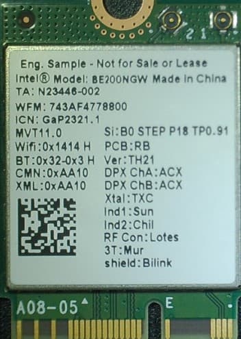
PD9BE200NG
Sep 13, 2023Intel BE200
Equipment Class
6CD - 15E 6 GHz Low Power Dual Client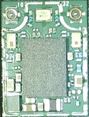
PD9BE200D2
Sep 13, 2023Intel BE200
Equipment Class
6CD - 15E 6 GHz Low Power Dual Client