PD9FJ3B2915ABGIntel PRO/Wireless 2915ABG Network Connection
Intel Corporation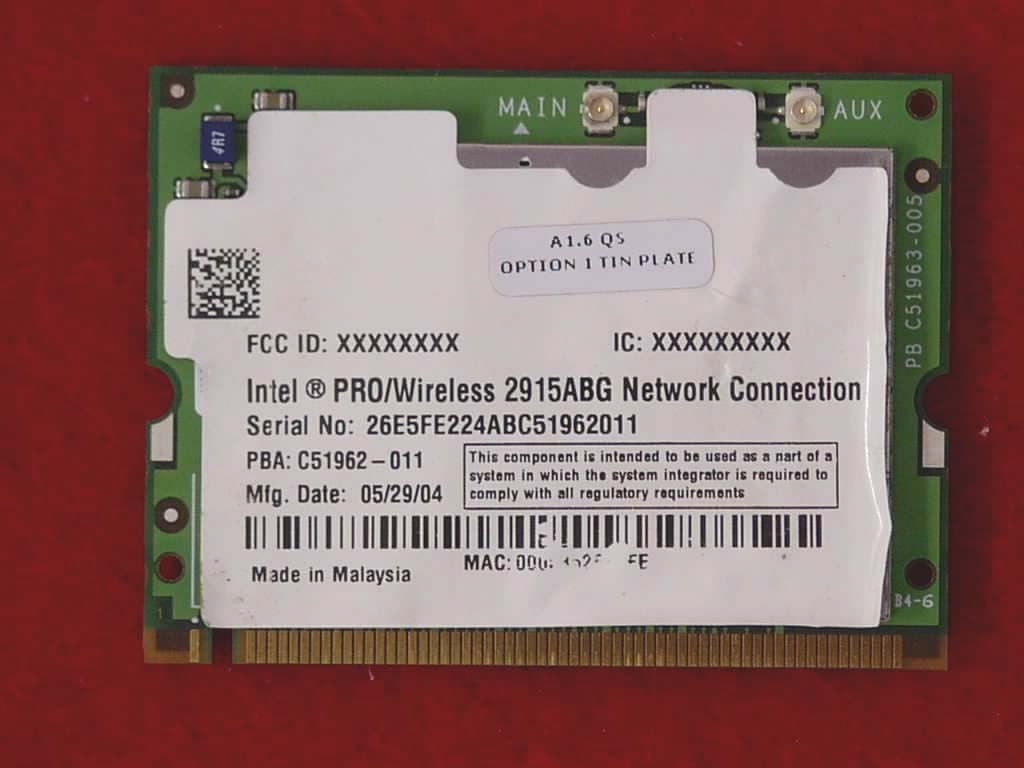
Click to zoom
Application Details
- Equipment Class
- NII - Unlicensed National Information Infrastructure TX
- Date of Grant
- Sep 21, 2004
- Application Purpose
- Original Equipment
- Date of Application
- Sep 21, 2004
- Equipment Note
- Intel PRO/Wireless 2915ABG Network Connection
- Frequency Range
- 5260.00000000 - 5320.00000000
- Company
- Intel Corporation
- Country
- France
Documents & Files
Document Text
Text extracted from the exhibit documents filed with the FCC. Open a document above to read the original.
Users Manual
Contents Intel(R) PRO/Wireless 2915ABG Network Connection User Guide With your wireless network card, you can access wireless networks, share files or printers, or even share your Internet connection. All of these features can be explored using a wireless network in your home or office. This wireless LAN solution is designed for both home and business use. Additional users and features can be added as your networking needs grow and change. Your Intel(R) PROSet/Wireless 2915ABG Network Connection adapter is compatible with 802.11a, 802.11b or 802.11g wireless standards. Operating at 5 GHz or 2.4 GHz frequency at speeds of up to 54 Mbps you can now connect your computer to existing high-speed networks using multiple access points within large or small environments. Your wireless adapter maintains automatic data rate control according to access point location to achieve the fastest possible connection. provide enhanced security measures using 802.1x network authentication. All of your wireless networks connections can be easily managed by Intel PROSet/Wireless. Intel(R) PRO/Wireless profiles provide enhanced security measures using 802.1x network authentication. NOTE: The software is compatible with the Intel PROSet/Wireless 2915ABG Network Connection and the Intel PROSet Wireless 2200BG Network Connection. Table of Contents l Using Intel PROSet/Wireless l Using Profiles l Setting up Security l Security Overview l Introduction to Wireless Networking l Connecting to a Network l Specifications l Troubleshooting l Glossary l Customer Support l Safety and Regulatory Information l Warranty l Adapter Registration Information in this document is subject to change without notice. file:///C|/CX2%20Muroc%20UG/6-15-04/index.htm (1 of 2) [6/15/2004 3:40:01 PM] Contents © 2000–2004 Intel Corporation. All rights reserved. Intel Corporation, 5200 N.E. Elam Young Parkway, Hillsboro, OR 97124-6497 USA The copying or reproducing of any material in this document in any manner whatsoever without the written permission of Intel Corporation is strictly forbidden. Intel(R) is a trademark or registered trademark of Intel Corporation or its subsidiaries in the United States and other countries. Other trademarks and trade names may be used in this document to refer to either the entities claiming the marks and names or their products. Intel disclaims any proprietary interest in trademarks and trade names other than its own. Microsoft and Windows are registered trademarks of Microsoft Corporation. *Other names and brands may be claimed as the property of others. Intel Corporation assumes no responsibility for errors or omissions in this document. Nor does Intel make any commitment to update the information contained herein. June 2004 file:///C|/CX2%20Muroc%20UG/6-15-04/index.htm (2 of 2) [6/15/2004 3:40:01 PM] Using Intel(R)PROSet/Wireless Back to Contents Using Intel PROSet/Wireless Software: Intel(R) PRO/Wireless 2915ABG Network Connection User Guide l Using Intel(R) PROSet/Wireless as your Wireless Manager l Starting Intel PROSet/Wireless l Launch Intel PROSet/Wireless from the task tray l Task Tray Menu Options l Tool Tips and Balloon Message Prompts l Intel PROSet/Wireless Main Window l Connection Status Icons l Connection Details l Profile List l Available Networks l Menus (Tools and Profile menus) l Tools Menu m Application Settings m Adapter Settings m Use Microsoft Client m Advanced Statistics m Intel Wireless Troubleshooter m Administrator Tool l Profiles Menu m Import/Export m Manage Exclusions l Enabling and Disabling the Radio l Installing and Uninstalling the Software l Installing and Uninstalling Single Sign On Feature Using Intel(R) PROSet/Wireless as your Wireless Manager Intel PROSet/Wireless can be used to setup, edit and manage network profiles to connect to a network. It also includes advanced settings such as power management and channel selection for setting up ad-hoc networks. If you are using Windows XP as your wireless manager, you can disable it from the Wireless Network tab. To disable Windows XP as your wireless manager: 1. Double-click the Intel PROSet/Wireless icon in the desktop task tray or click Start ‡Settings ‡Control Panel and double-click on Network Connections. 2. Right-click Wireless Network Connection and click Properties. 3. Click on Wireless Networks tab on the Wireless Network Connection Properties. 4. Verify that the Use Windows to configure my wireless network settings box is not selected. If it is, deselect it. 5. Click OK. This confirms that the Intel PROSet/Wireless utility is configured to manage your network profiles. file:///C|/CX2%20Muroc%20UG/6-15-04/assist.htm (1 of 32) [6/15/2004 3:40:06 PM] Using Intel(R)PROSet/Wireless NOTE: Check that the Application Settings option Notify me when another application is using the wireless device is selected. This option prompts you when Windows XP starts to manage your network profiles. Starting Intel PROSet/Wireless Launch Intel PROSet/Wireless either from the task tray icon, the Windows Start button, or from the Windows Control Panel icon. To launch Intel PROSet/Wireless use either of the following methods: l Click Start > Programs > Intel Wireless > Intel PROSet/Wireless. l Right-click the task tray icon located in the lower right corner of your Windows Desktop, and click the menu option Open Intel PROSet/Wireless. l Double-click the task tray icon to open Intel PROSet/Wireless. Exit Intel PROSet/Wireless: l To exit Intel PROSet/Wireless and close the task tray icon, click Exit from the from the task tray menu or click the Close button on the Intel PROSet/Wireless main window. Launch Intel PROSet/Wireless from the task tray To launch Intel PROSet/Wireless, double-click the task tray icon located in the lower right corner of your Windows desktop or right-click the task tray icon and click Open Intel PROSet/Wireless. Exit Intel PROSet/Wireless To exit Intel PROSet/Wireless and hide the task tray icon, right-click the task tr…
Text truncated - open the document above for the full version.
Cover Letter(s)
AEGIS LABS, INC 22431 Antonio Parkway B160-417, Rancho Santa Margarita, CA 92688 949-459-7886 TEL 949-459-7869 FAX www.aegislabsinc.com TRANSMITTER MODULAR APPROVAL ATTESTATION September 02, 2004 Federal Communications Commission Re: Application Modular Approval Certification for FCC ID: PD9FJ3B2915ABG Gentlemen: The following attestation addresses the eight requirements to support modular approval as required by the FCC Public Notice DA00-1407 “Part 15 Unlicensed Modular Transmitter Approval” 1 The modular transmitter has its own RF shielding and does not rely upon the shielding provided by the device into which it is installed in order to comply with Part 15 limits. 2 The modular transmitter has buffered modulation/data inputs. All inputs to the modules are buffered through the radio circuitry. 3 The modular transmitter has its own power supply regulator. 4 The modular transmitter has an antenna that complies with section 15.203 and 15.204(c) of the FCC rules. It has a UFL type of connector at the transmitter end and is soldered to the antenna (depending on OEM configuration). Also the antenna will be internal in the OEM host equipment and inaccessible to the user. 5 The modular transmitter was tested outside of a host desktop computer using a PCI extender card. The PCI extender card allows the transmitter to be placed outside of the chassis of the host desktop computer. 6 The modular transmitter will be labeled with its own FCC ID. Also, the OEM host computer manufacturer will be informed to display a label referring to the enclosed module. The exterior label will read as follows: “Contains Transmitter Module FCC ID” or “Contains TXFCCID”. 7 The modular transmitter is manufactured so that the user cannot influence the operation of the transmitter that will operate outside of the scope of the regulations. 8 The modular transmitter meets the MPE calculations of 47 CFR 1.1307(b)(1). Also, SAR data is available if necessary. If there are any additional questions or if further information is needed, please contact us at your earliest convenience at (949) 459-7886. Sincerely, Rick Candelas Aegis Labs, Inc. Lab Manager
Cover Letter(s)
September 15, 2004 RE: Intel Corporation FCC ID: PD9FJ3B2915ABG Answers to the ATCB comments on the above referenced Application. 1) The channel attestation provided appears to list the incorrect FCC ID number. Please verify the model number information as well. Please refer to “PD9FJ3B2915ABG Channel Attestation.pdf” exhibit. The model names are correct. The only change is the FCC ID. 2) Power listed on page 12 of the theory of operation suggests higher power than measured. Please explain if this page is the intended TX power or not. Note that the FCC expects the device to be TX at the highest output power possible. Please refer to “Theory of Operation - WM3B2915ABG (Revised).pdf” exhibit. The power levels were revised. 3) Please note that the FCC no longer desires that the safe distance for mobile devices be calculated in the RF exposure exhibit if the safe distance is < 20 cm, but instead prefers the power density results to be calculated at 20 cm and compared to the power density limit. Please refer to “MPE Calculations (Rev. A, 09-16-04).doc” exhibit. 4) Regarding the MPE calculations, it appears that the maximum gain for Pumpkin antenna in the 2.4 GHz band is actually 2.31 dBi, not 2.65 dBi. Please review and correct if necessary. Please refer to “MPE Calculations (Rev. A, 09-16-04).doc” exhibit. 5) Regarding the MPE calculations, it appears that the maximum gain for Pumpkin antenna in the 5 GHz band is actually 2.95 dBi, not 2.65 dBi. Please review and correct if necessary. Please refer to “MPE Calculations (Rev. A, 09-16-04).doc” exhibit. 6) Photographs of the antennas provided in the antenna information appear to be much different in size/shape than the test photographs. Please explain. Please refer to “Photographs - Test Setup (Rev. A, 09-16-04).doc” exhibit. The antennas are mounted on the upper corners on the LCD screens. 7) Gains in the test report for the Mint and Pumpkin antenna do not appear to match the antenna information provided. Please refer to test report revisions. Page 8 of the DTS report and page 7 of the UNII report. 8) Limits on page 33 & 34 of the DTS test report do not appear correct (60 and 80 dBuV/m). These limits also appear many times elsewhere in the DTS report and throughout the UNII report but is uncertain what these are. Please explain the derivation of these and/or correct as necessary. These limits are from Table 3 in RSS-210 for the receiver mode of operation of the EUT. 9) Please explain the derivation of the 68 dBuV/m limits on pages 31 & 32 of the DTS report. Note this is duplicated throughout the report. This appears to be the limit is for the -27 dBm UNII limit, although this is a DTS report. Please explain. That was a mistake. The limit should have been –20dB below the carrier frequency. Please refer to test report revisions.
Cover Letter(s)
American Telecommunications Certification Body Inc. 6731 Whittier Ave, McLean, VA 22101 August 27, 2004 RE: Intel Corporation FCC ID: PD9FJ3B2915ABG After a review of the submitted information, I have a few comments on the above referenced Application. Administrative Issues: 1) The channel attestation provided appears to list the incorrect FCC ID number. Please verify the model number information as well. 2) Power listed on page 12 of the theory of operation suggests higher power than measured. Please explain if this page is the intended TX power or not. Note that the FCC expects the device to be TX at the highest output power possible. 3) Please note that the FCC no longer desires that the safe distance for mobile devices be calculated in the RF exposure exhibit if the safe distance is < 20 cm, but instead prefers the power density results to be calculated at 20 cm and compared to the power density limit. 4) Regarding the MPE calculations, It appears that the maximum gain for Pumpkin antenna in the 2.4 GHz band is actually 2.31 dBi, not 2.65 dBi. Please review and correct if necessary. 5) Regarding the MPE calculations, It appears that the maximum gain for Pumpkin antenna in the 5 GHz band is actually 2.95 dBi, not 2.65 dBi. Please review and correct if necessary. 6) Photographs of the antennas provided in the antenna information appear to be much different in size/shape than the test photographs. Please explain. --- Continued on Next Page --- z Page 2 September 15, 2004 --- Continued on Next Page --- z Page 3 September 15, 2004 7) Gains in the test report for the Mint and Pumpkin antenna do not appears to match the antenna information provided. 8) Limits on page 33 & 34 of the DTS test report do not appear correct (60 and 80 dBuV/m). These limits also appear many times elsewhere in the DTS report and throughout the UNII report but is uncertain what these are. Please explain the derivation of these and/or correct as necessary. 9) Please explain the derivation of the 68 dBuV/m limits on pages 31 & 32 of the DTS report. Note this is duplicated throughout the report. This appears to be the limit is for the -27 dBm UNII limit, although this is a DTS report. Please explain. Timothy R. Johnson Examining Engineer mailto: [email protected] The items indicated above must be submitted before processing can continue on the above referenced application. Failure to provide the requested information may result in application termination. Correspondence should be considered part of the permanent submission and may be viewed from the Internet after a Grant of Equipment Authorization is issued. Please do not respond to this correspondence using the email reply button. In order for your response to be processed expeditiously, you must submit your documents through the AmericanTCB.com website. Also, please note that partial responses increase processing time and should not be submitted. Any questions about the content of this correspondence should be directed to the sender.
External Photos
Top View Bottom View
ID Label/Location Info
IC: 1000M-FJ2915 FCC ID: PD9FJ3B2915ABG
Internal Photos
Top View “Insulation removed” Bottom View “Insulation removed” Top View “Shielding removed”
RF Exposure Info
Antenna Summary (Reversed-F Antenna) Antenna Type Reversed-F Antenna Cable type ( length ) Coax( about 500mm ) P/N Left : 2576965 Right : 2576957 Gain MAX : 0.39(dBi) *see Note * Note: 1. Included all cable losses. Picture: T About 280mm Antenna Position About 270mm
RF Exposure Info
[Mint,Mint2,Mint3,Mint4 Antenna]1/14 Mint(Mint2,Mint3,Mint4) Antenna Data 1A1D1E1F1G1H Antenna Part NumberCable Assembly Part Number and Information Peak Gain W/i Cable loss (dBi) Peak Gain w/o Cable Loss (dBi) VSWRCable Loss (dBi) (P/N:YCE-5008) 2400- 2500MHz 2400- 2500MHz 2400- 2500MHz 2400- 2500MHz Main antenna Yokowo Co.Ltd Monopole(P/N: U.FL-2LP -5016-A-480) 0.81 dBi (peak) 2.11 dBi (peak) 1.20 max1.30 dBi (peak) 50 ohm Coaxial.5150- 5350MHz 5150- 5350MHz 5150- 5350MHz 5150- 5350MHz Right length: 48cm-0.26 dBi (peak) 1.74 dBi (peak) 2.10 max2.00 dBi (peak) diameter: 1.1mm5470- 5725MHz 5470- 5725MHz 5470- 5725MHz 5470- 5725MHz Connector: U.FL-1.62 dBi (peak) 0.38 dBi (peak) 2.40 max2.00 dBi (peak) 5725- 5850MHz 5725- 5850MHz 5725- 5850MHz 5725- 5850MHz 1.45 dBi (peak) 3.45 dBi (peak) 2.50 max2.00 dBi (peak) (P/N:YCE-5008)Example: 2400- 2500MHz 2400- 2500MHz 2400- 2500MHz 2400- 2500MHz Auxiliary antennaYokowo Co.Ltd Monopole(P/N: U.FL-2LP -5016-A-410) 2.85 dBi (peak) 4.15 dBi (peak) 1.20 max1.30 dBi (peak) 50 ohm Coaxial.5150- 5350MHz 5150- 5350MHz 5150- 5350MHz 5150- 5350MHz Left length: 41cm0.63 dBi (peak) 2.63 dBi (peak) 2.50 max2.00 dBi (peak) diameter: 1.1mm5470- 5725MHz 5470- 5725MHz 5470- 5725MHz 5470- 5725MHz Connector: U.FL-1.69 dBi (peak) 0.31 dBi (peak) 2.80 max2.00 dBi (peak) 5725- 5850MHz 5725- 5850MHz 5725- 5850MHz 5725- 5850MHz -0.16 dBi (peak) 1.84 dBi (peak) 2.90 max2.00 dBi (peak) 1B Manufacture 1C Antenna Type [Mint,Mint2,Mint3,Mint4 Antenna] 2/14 Ceramic antenna test data Application : For W-LAN (IEEE-802.11a,b,g) Measurement institution : Yokowo No.3 radio measuring site Antenna model : YCE-5008 Date : 2003/3/20 Measurement condition : Mint,Mint2,Mint3,Mint4 (Disp. Upper Left) Measured by : S.Yoshida Antenna matching : Shunt L (2.2nH) Correction of cable loss : Non (include loss 1.3dB) f=2400MHz Peak. gain A verage gain Tx H & V average Each frequency average [dBi] [dBi] [dBi] [dBi] Horizontal 0.74 -5.67 Vertical -3.28 -8.87 Horizontal 0.26 -6.51 Vertical -1.55 -9.08 Horizontal -9.83 -14.47 Vertical -4.59 -9.55 f=2442MHz VSWR Peak. gain A verage gain Tx H & V average Each frequency average [dBi] [dBi] [dBi] [dBi] Horizontal 0.39 -5.69 Vertical -2.70 -8.59 Horizontal 0.81 -5.64 Vertical -1.41 -8.38 Horizontal -6.71 -11.63 Vertical -5.63 -10.73 f=2484MHz Peak. gain A verage gain Tx H & V average Each frequency average [dBi] [dBi] [dBi] [dBi] Horizontal 0.17 -5.73 Vertical -2.57 -8.35 Horizontal 0.80 -5.17 Vertical -1.44 -8.00 Horizontal -6.27 -11.04 Vertical -3.97 -9.03 1112, Kanohara, Tomioka-shi Gunma, 370-2495, JAPAN Personal Communication Antenna TEL +81 274-62-2127 FAX +81 274-62-2031 Plane Tx X-Y -7.0 Y-Z -7.6 -8.3 Z-X -11.3 Plane Tx X-Y -6.9 Z-X -9.9 X-Y -6.8 Y-Z -6.4 -7.9 Z-X -11.2 -7.4 Plane Tx Y-Z -6.8 dBi To : FUJITSU LIMITED -10.8 -7.8 X-Y plane all average (all frequency) Y-Z plane all average (all frequency)Z-X plane all average (all frequency) All plane & all frequency average -6.9-6.9 dBidBidBi [Mint,Mint2,Mint3,Mint4 Antenna] 3/14 Ceramic antenna test data Application : For W-LAN (IEEE-802.11a,b,g) Measurement institution : Yokowo No.3 radio measuring site Antenna model : YCE-5008 Date : 2003/3/20 Measurement condition : Mint,Mint2,Mint3,Mint4 (Disp. Upper Left) Measured by : S.Yoshida Antenna matching : Shunt L (2.2nH) Correction of cable loss : Non (include loss 2.0dB) f=4900MHz Peak. gain A verage gain Tx H & V average Each frequency average [dBi] [dBi] [dBi] [dBi] Horizontal -0.33 -4.79 Vertical -2.03 -7.13 Horizontal -0.26 -5.18 Vertical -1.89 -7.71 Horizontal -3.50 -10.05 Vertical -1.55 -6.75 f=5350MHz VSWR Peak. gain A verage gain Tx H & V average Each frequency average [dBi] [dBi] [dBi] [dBi] Horizontal -1.62 -6.39 Vertical -5.03 -10.59 Horizontal -2.04 -6.74 Vertical -3.76 -9.97 Horizontal -3.76 -10.09 Vertical -3.09 -8.57 f=5825MHz Peak. gain A verage gain Tx H & V average Each frequency average [dBi] [dBi] [dBi] [dBi] Horizontal 0.96 -4.43 Vertical -3.31 -8.94 Horizontal 0.61 -4.63 Vertical -5.25 -10.12 Horizontal -4.22 -9.47 Vertical 1.45 -2.59 1112, Kanohara, Tomioka-shi Gunma, 370-2495, JAPAN Personal Communication Antenna TEL +81 274-62-2127 FAX +81 274-62-2031 -5.8 Z-X -4.8 X-Y -6.1 Y-Z -6.6 Z-X -9.3 Plane Tx Z-X plane all average (all frequency) -7.0 Plane Tx X-Y -8.0 Y-Z -8.1 -8.4 -6.9 dBi dBi Y-Z -6.3 -6.6 Z-X -8.1 All plane & all frequency average -6.8 dBi Plane Tx X-Y plane all average (all frequency) -6.5 dBi X-Y -5.8 Y-Z plane all average (all frequency) [Mint,Mint2,Mint3,Mint4 Antenna] 4/14 Ceramic antenna test data Measurement condition Field pattern X-Y plane Antenna coordinated 1112, Kanohara, Tomioka-shi Gunma, 370-2495, JAPAN Personal Com munication Antenna TEL +81 274-62-2127 FAX +81 274-62-2031 2.5m 4m DUT Tx:W ridged horn Antenna X Y -45.0-35.0-25.0-15.0 -5.0 5.0 [Deg] 0 180 -90 90 ① -45.0-35.0-25.0-15.0 -5.0 5.0 [Deg] 0 180 -90 90 ② -45.0-35.0-25.0-15.0 -5.0 5.0 [Deg] 0 180 -90 90 ③ -45.0-35.0-25.0-15.0 -5.0 5.0 [Deg] 0 180 -90 90 ④ -45.0-35.0-25.0-15.0 -5.0 5.0 [Deg] 0 180 -90 90 ⑤ -45.0-35.0-25.0-15.0 -5.0 5.0 [Deg] 0 180 -90 90 ⑥ Line No. Frequency[MHz] MEMO MAX. Gain[dBi] AVG. Gain[dBi] 1 ① 2400.00 Tx-H 0.74 -5.67 2 ① 2400.00 Tx-V -3.28 -8.87 3 ② 2442.00 Tx-H 0.39 -5.69 4 ② 2442.00 Tx-V -2.70 -8.59 5 ③ 2484.00 Tx-H 0.17 -5.73 6 ③ 2484.00 Tx-V -2.57 -8.35 7 ④ 4900.00 Tx-H -0.33 -4.79 8 ④ 4900.00 Tx-V -2.03 -7.13 9 ⑤ 5350.00 Tx-H -1.62 -6.39 10 ⑤ 5350.00 Tx-V -5.03 -10.59 11 ⑥ 5825.00 Tx-H 0.96 -4.43 12 ⑥ 5825.00 Tx-V -3.31 -8.94 Fj - 030320 - 005 .ant S.Yoshida03/03/20Mint with YCE-5008 L-ANT X-Y All AVG.All MAX. AVG. -6.72[dBi]-1.18[dBi] X Y Z [Mint,Mint2,Mint3,Mint4 Antenna] 5/14 Ceramic antenna test data Field pattern Y-Z plane Field pattern Z-X plane 1112, Kanohara, Tomioka-shi Gunma, 370-2495, JAPAN Personal Com munication Antenna TEL +81 274-62-2127 FAX +81 274-62-2031 -45.0-35.0-25.0-15.0 -5.0 5.0 [Deg] 0 180 -90 90 ① -45.0-35.0-25.0-15.0 -5.0 5.0 [Deg] 0 180 -90 90 ② -45.0-35.0-25.0-15.0 -5.0 5.0 [Deg] 0 1…
Text truncated - open the document above for the full version.
RF Exposure Info
[Pumpkin/Pumpkin2]1/14 Pumpkin/Pumpkin2 Antenna Data 1A1D1E1F1G1H Antenna Part NumberCable Assembly Part Number and Information Peak Gain W/i Cable loss (dBi) Peak Gain w/o Cable Loss (dBi) VSWRCable Loss (dBi) (P/N:YCE-5008) 2400- 2500MHz 2400- 2500MHz 2400- 2500MHz 2400- 2500MHz Main antenna Yokowo Co.Ltd Monopole(P/N: U.FL-2LP -5016-A-340) 2.29 dBi (peak) 3.69dBi (peak) 1.16 max1.4dBi (peak) 50 ohm Coaxial.5150- 5350MHz 5150- 5350MHz 5150- 5350MHz 5150- 5350MHz Right length: 34cm2.65 dBi (peak) 4.65 dBi (peak) 2.15 max2.00 dBi (peak) diameter: 1.1mm5470- 5725MHz 5470- 5725MHz 5470- 5725MHz 5470- 5725MHz Connector: U.FL0.54 dBi (peak) 2.54 dBi (peak) 2.50 max2.00 dBi (peak) 5725- 5850MHz 5725- 5850MHz 5725- 5850MHz 5725- 5850MHz 2.95 dBi (peak) 4.95 dBi (peak) 2.40 max2.00 dBi (peak) (P/N:YCE-5008)Example: 2400- 2500MHz 2400- 2500MHz 2400- 2500MHz 2400- 2500MHz Auxiliary antennaYokowo Co.Ltd Monopole(P/N: U.FL-2LP -5016-A-480) 2.31dBi (peak) 3.51dBi (peak) 2.00 max1.2 dBi (peak) Left 50 ohm Coaxial.5150- 5350MHz 5150- 5350MHz 5150- 5350MHz 5150- 5350MHz length: 48cm1.98 dBi (peak) 3.98 dBi (peak) 2.00 max2.00 dBi (peak) diameter: 1.1mm5470- 5725MHz 5470- 5725MHz 5470- 5725MHz 5470- 5725MHz Connector: U.FL1.80 dBi (peak) 3.80 dBi (peak) 2.60 max2.00 dBi (peak) 5725- 5850MHz 5725- 5850MHz 5725- 5850MHz 5725- 5850MHz 2.17 dBi (peak) 4.17 dBi (peak) 2.30 max2.00 dBi (peak) 1B Manufacture 1C Antenna Type [Pumpkin/Pumpkin2] 2/14 Ceramic antenna test data Application : For W-LAN (IEEE-802.11a,b,g) Measurement institution : Yokowo No.3 radio measuring site Antenna model : YCE-5008 (008L00197) Date : 2004/02/11 Measurement condition : Pumpkin(Pumpkin2) Disp.-left side Measured by : S.Yoshida Antenna matching : Shunt L (2.2nH) Correction of cable loss : Non (include loss 1.4dB) f=2400MHz Peak. gain A verage gain Tx H & V average Each frequency average [dBi] [dBi] [dBi] [dBi] Horizontal -0.36 -6.35 Vertical -1.58 -7.09 Horizontal 1.33 -4.98 Vertical -2.69 -7.80 Horizontal -1.77 -10.94 Vertical -3.23 -8.83 f=2442MHz VSWR Peak. gain A verage gain Tx H & V average Each frequency average [dBi] [dBi] [dBi] [dBi] Horizontal 0.68 -6.28 Vertical -1.10 -6.88 Horizontal 2.29 -4.62 Vertical -1.23 -7.32 Horizontal -2.44 -11.08 Vertical -1.91 -6.93 f=2484MHz Peak. gain A verage gain Tx H & V average Each frequency average [dBi] [dBi] [dBi] [dBi] Horizontal 0.69 -6.31 Vertical -1.14 -6.92 Horizontal 2.00 -5.08 Vertical -1.13 -7.66 Horizontal -2.59 -10.14 Vertical -3.20 -7.91 1112, Kanohara, Tomioka-shi Gunma, 370-2495, JAPAN Antenna Engineering Dept. TEL +81 274-62-2127 FAX +81 274-62-2031 dBidBidBidBi To : FUJITSU LIMITED -9.0-7.0 X-Y plane all average (all frequency) Y-Z plane all average (all frequency)Z-X plane all average (all frequency) All plane & all frequency average -6.6-6.0 -6.8 Z-X -8.5 -7.1 Plane Tx Y-Z -5.8 Z-X -8.9 X-Y -6.6 Y-Z -6.2 Plane Tx X-Y -6.6 Y-Z -6.2 -7.3 Z-X -9.8 Plane Tx X-Y -6.7 [Pumpkin/Pumpkin2] 3/14 Ceramic antenna test data Application : For W-LAN (IEEE-802.11a,b,g) Measurement institution : Yokowo No.3 radio measuring site Antenna model : YCE-5008 (008L00197) Date : 2004/02/11 Measurement condition : Pumpkin(Pumpkin2) Disp.-left side Measured by : S.Yoshida Antenna matching : Shunt L (2.2nH) Correction of cable loss : Non (include loss 2dB) f=4900MHz Peak. gain A verage gain Tx H & V average Each frequency average [dBi] [dBi] [dBi] [dBi] Horizontal 0.96 -5.06 Vertical 0.61 -4.69 Horizontal 2.65 -3.56 Vertical -0.77 -7.78 Horizontal -0.80 -7.49 Vertical -1.55 -4.82 f=5350MHz VSWR Peak. gain A verage gain Tx H & V average Each frequency average [dBi] [dBi] [dBi] [dBi] Horizontal -0.49 -5.79 Vertical -0.87 -6.75 Horizontal 0.54 -4.20 Vertical -2.51 -8.83 Horizontal -2.62 -8.24 Vertical -3.69 -8.56 f=5825MHz Peak. gain A verage gain Tx H & V average Each frequency average [dBi] [dBi] [dBi] [dBi] Horizontal 1.04 -4.53 Vertical 1.48 -5.42 Horizontal 2.95 -2.69 Vertical -1.54 -8.50 Horizontal -0.37 -5.94 Vertical 1.03 -3.37 1112, Kanohara, Tomioka-shi Gunma, 370-2495, JAPAN Antenna Engineering Dept. TEL +81 274-62-2127 FAX +81 274-62-2031 dBi Plane Tx X-Y plane all average (all frequency) -5.3 dBi X-Y -4.9 Y-Z plane all average (all frequency) -5.2 dBi dBi Y-Z -5.2 -5.3 Z-X -6.0 All plane & all frequency average -5.5 Z-X plane all average (all frequency) -6.0 Plane Tx X-Y -6.2 Y-Z -5.9 -6.7 Z-X -8.4 Plane Tx -4.7 Z-X -4.5 X-Y -5.0 Y-Z -4.7 [Pumpkin/Pumpkin2] 4/14 Ceramic antenna test data Measurement condition Field pattern X-Y plane Antenna coordinated 1112, Kanohara, Tomioka-shi Gunma, 370-2495, JAPAN Antenna Engineering Dept. TEL +81 274-62-2127 FAX +81 274-62-2031 2.5m 4m DUT Tx:W ridged horn Antenna X Y -45.0-35.0-25.0-15.0 -5.0 5.0 [Deg] 0 180 -90 90 ① -45.0-35.0-25.0-15.0 -5.0 5.0 [Deg] 0 180 -90 90 ② -45.0-35.0-25.0-15.0 -5.0 5.0 [Deg] 0 180 -90 90 ③ -45.0-35.0-25.0-15.0 -5.0 5.0 [Deg] 0 180 -90 90 ④ -45.0-35.0-25.0-15.0 -5.0 5.0 [Deg] 0 180 -90 90 ⑤ -45.0-35.0-25.0-15.0 -5.0 5.0 [Deg] 0 180 -90 90 ⑥ Line No. Frequency[MHz] MEMO MAX. Gain[dBi] AVG. Gain[dBi] 1 ① 2400.00 Tx-H -0.36 -6.35 2 ① 2400.00 Tx-V -1.58 -7.09 3 ③ 2442.00 Tx-H 0.68 -6.28 4 ③ 2442.00 Tx-V -1.10 -6.88 5 ⑤ 2484.00 Tx-H 0.69 -6.31 6 ⑤ 2484.00 Tx-V -1.14 -6.92 7 ② 4900.00 Tx-H 0.96 -5.06 8 ② 4900.00 Tx-V 0.61 -4.69 9 ④ 5350.00 Tx-H -0.49 -5.79 10 ④ 5350.00 Tx-V -0.87 -6.75 11 ⑥ 5825.00 Tx-H 1.04 -4.53 12 ⑥ 5825.00 Tx-V 1.48 -5.42 Fj-040211-009.antS.Yoshida04年02月11日Pampukin Disp.左 X-Y All AVG.All MAX. AVG. -5.92[dBi]0.10[dBi] [Pumpkin/Pumpkin2] 5/14 Ceramic antenna test data Field pattern Y-Z plane Field pattern Z-X plane 1112, Kanohara, Tomioka-shi Gunma, 370-2495, JAPAN Antenna Engineering Dept. TEL +81 274-62-2127 FAX +81 274-62-2031 Y Z X Z -45.0-35.0-25.0-15.0 -5.0 5.0 [Deg] 0 180 -90 90 ① -45.0-35.0-25.0-15.0 -5.0 5.0 [Deg] 0 180 -90 90 ② -45.0-35.0-25.0-15.0 -5.0 5.0 [Deg] 0 180 -90 90 ③ -45.0-35.0-25.0-15.0 -5.0 5.0 [Deg] 0 180 -90 90 ④ -45.0-35.0-25.0-15.0 -5.0 5.0 [Deg] 0 180 -90 90 ⑤ -45.0-35.0-25.0-1…
Text truncated - open the document above for the full version.
RF Exposure Info
[Emilia,Emilia2 Antenna]1/5 Antenna SummaryEmilia,Emilia2 Designator ManufactureFujitsu Antenna TypeInverted-F Antenna Cable type ( length )Coax( about 600mm ) P/N CP115412-01 L side CP115412-01 R side Gain Picture: Front View 4.9-5.8GHz MAX : 1.18(dBi) *see Note 2.4-2.48GHz MAX : 1.06(dBi) *see Note Note:Note that the maximum(peak) antenna gain includes all cable losses. 250mm L Antenna R Antenna 310 mm 285 mm [Emilia,Emilia2 Antenna]2/5 Rear View L Antenna R Antenna [Emilia,Emilia2 Antenna]3/5 [Emilia,Emilia2 Antenna]4/5 [Emilia,Emilia2 Antenna]5/5 Left-Side Antenna Right-Side Antenna
RF Exposure Info
MPE Calculations Systems operating under the provision of 47 CFR 1.1307(b)(1) shall be operated in a manor that ensures that the public is not exposed to radio frequency energy levels in excess of the FCC guidelines. The EUT will only be used with a separation of 20 centimeters or greater between the antenna and the body of the user or nearby persons and can therefore be considered a mobile transmitter per 47 CFR 2.1091(b). The MPE calculation for this exposure is shown below. Using the Yokowo (Pumpkin) Antennas @ 5 GHz Range with highest output power: The peak radiated output power (EIRP) is calculated as follows: EIRP = P + G EIRP = 23.30 dBm + 2.95 dBi EIRP = 26.25 dBm (421.69 mW) Where P = Power input to the antenna (mW). G = Power gain of the antenna (dBi) Power density at the specific separation: S = PG/(4R 2 π) S = (213.80 x 1.97) / (4 x 20 2 x π) S = 0.083 mW/cm 2 Where S = Maximum power density (mW/cm 2 ) P = Power input to the antenna (mW). G = Numeric power gain of the antenna R = Distance to the center of the radiation of the antenna (20cm = limit for MPE) The maximum permissible exposure (MPE) for the general population is 1mW/cm 2 . The power density at 20cm does not exceed the 1mW/cm 2 limit. Therefore, the exposure condition is compliant with FCC rules. The numeric gain (G) of the antenna with a gain specified in dB is determined by: G = Log -1 (dB antenna gain/10) G = Log -1 (2.95 dBi/10) G = 1.97 Using the Yokowo (Pumpkin) Antennas @ 2.4 GHz Range with highest output power: The peak radiated output power (EIRP) is calculated as follows: EIRP = P + G EIRP = 24.10 dBm + 2.31 dBi EIRP = 26.41 dBm (437.52 mW) Where P = Power input to the antenna (mW). G = Power gain of the antenna (dBi) Power density at the specific separation: S = PG/(4R 2 π) S = (257.10 x 1.70) / (4 x 20 2 x π) S = 0.087 mW/cm 2 Where S = Maximum power density (mW/cm 2 ) P = Power input to the antenna (mW). G = Numeric power gain of the antenna R = Distance to the center of the radiation of the antenna (20cm = limit for MPE) The maximum permissible exposure (MPE) for the general population is 1mW/cm 2 . The power density at 20cm does not exceed the 1mW/cm 2 limit. Therefore, the exposure condition is compliant with FCC rules. The numeric gain (G) of the antenna with a gain specified in dB is determined by: G = Log -1 (dB antenna gain/10) G = Log -1 (2.31 dBi/10) G = 1.70 Using the Yokowo (Mint) Antennas @ 5 GHz Range with highest output power: The peak radiated output power (EIRP) is calculated as follows: EIRP = P + G EIRP = 23.30 dBm + 1.45 dBi EIRP = 24.75 dBm (298.53 mW) Where P = Power input to the antenna (mW). G = Power gain of the antenna (dBi) Power density at the specific separation: S = PG/(4R 2 π) S = (213.80 x 1.39) / (4 x 20 2 x π) S = 0.059 mW/cm 2 Where S = Maximum power density (mW/cm 2 ) P = Power input to the antenna (mW). G = Numeric power gain of the antenna R = Distance to the center of the radiation of the antenna (20cm = limit for MPE) The m…
Text truncated - open the document above for the full version.
Contact Information
Applicant
Benjamin Lavenant(Regulatory Engineer)
Technical Contact
Aegis Labs, Inc.Rick Candelas
[email protected]949-0459-7886
23091 Antonio Parkway, #B160-417 · Rancho Santa Margarita, California · United States
Non-Technical Contact
Aegis Labs, Inc.Rick Candelas
[email protected]949-0459-7886
Test Firm
Aegis Labs, Inc.Rick Candelas
Technical Specifications
| # | Rule Parts | Frequency Range | Power Output |
|---|---|---|---|
| 2 | 15E | 5.26 GHz - 5.32 GHz | 126.00 mW |
Other Applications from Intel Corporation
PD9BE201D2P
Aug 20, 2024Intel BE201D2WP
Equipment Class
NII - Unlicensed National Information Infrastructure TXPD9AX411NG
Jul 02, 2024Intel WiFi 6E AX411
Equipment Class
6CD - 15E 6 GHz Low Power Dual ClientPD9AX211D2H
Jan 28, 2024Intel Wi-Fi 6E AX211
Equipment Class
DSS - Part 15 Spread Spectrum Transmitter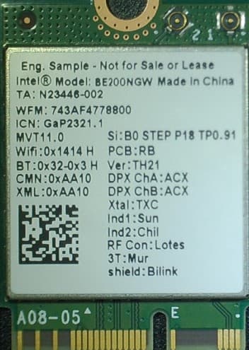
PD9BE200NG
Sep 13, 2023Intel BE200
Equipment Class
6CD - 15E 6 GHz Low Power Dual Client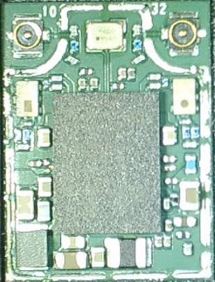
PD9BE200D2
Sep 13, 2023Intel BE200
Equipment Class
6CD - 15E 6 GHz Low Power Dual Client