PDHGMRS-3000BFRS/GMRS COMBINATION TRANSCEIVER
TTI Tech Co., Ltd.
Click to zoom
Application Details
- Equipment Class
- FRF - Part 95 Family Radio Face Held Transmitter
- Date of Grant
- Aug 21, 2002
- Application Purpose
- Original Equipment
- Date of Application
- Jul 09, 2002
- Equipment Note
- FRS/GMRS COMBINATION TRANSCEIVER
- Frequency Range
- 467.56250000 - 467.71250000
- Company
- TTI Tech Co., Ltd.
- Country
- South Korea
Documents & Files
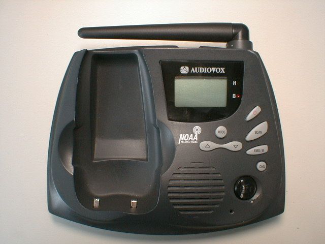
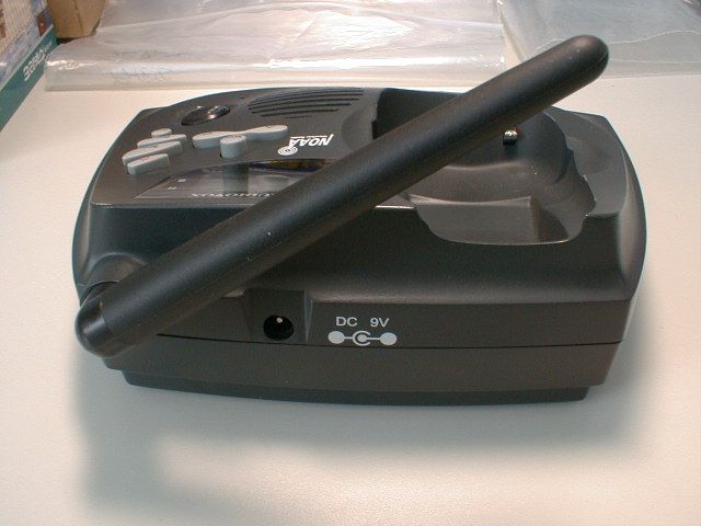
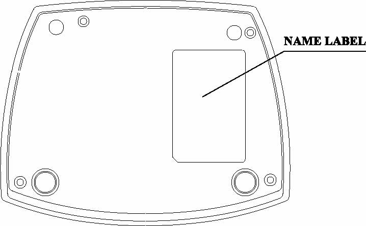
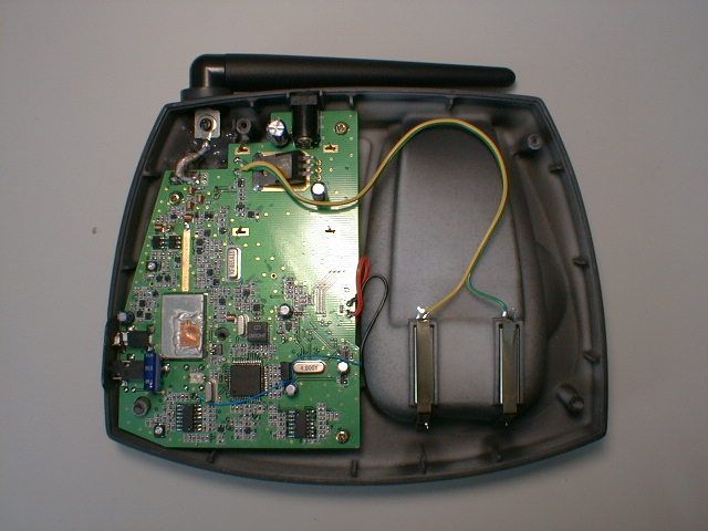
Document Text
Text extracted from the exhibit documents filed with the FCC. Open a document above to read the original.
Operational Description
Local oscillation frequency deviation. FL1 SAW filter or FL2 MCF fail. VCO circuit problem. -. Squelch does not work IF IC U2 problem. Control logic circuit problem. 5. DESCRIPTION OF RADIO CIRCUIT 5-1. Frequency synthesizer Frequency synthesizerconsists of VCO, loop filter and RFIC. RFIC includes MIX,IF, Compander and PLL. Frequency synthesizer uses the PLL of thte RFIC. a) VCO VCO is composed of ONE VCO Oscillation circuit takes colpitts circuit using variable Diode. The VCO generates GMRS frequencies and consists of L17, D5, C65, L19, C69, C70, R45, R44, R46, C71, C72, Q14, R47, C74, R48, Q15, L29, C147, C151. VCO control voltage through loop filter adjusts frequency and Microphone Signal through Modulation terminal makes modulation. N = VCO oscillation frequency / reference frequency If the desired frequency is 462.5625 MHz 1) TX : N = 462.5625 MHz / 0.00625 MHz = 74010 2) RX : N = [462.5625 MHz – 21.7 MHz] / 0.00625 MHz = 70538 A. PLL IC RFIC(PLL) is adjustable IC to produce the wished frequency which VCO provides through loop filter. It has internal counter using 21.25MHz. reference frequency to make 6.25kHz as reference Signal. VCO frequency from prescaled input is divided signal is compared with Reference signal phase in phase comparator. Built-in charger pump changes voltage (until two signals are in phase) and charged voltage supplies VCO through loop filter to produce the desired frequency. Frequency data associated with channel goes to PLL IC by CPU through CLOCK , DATA. PLL IC enables by strobe line of CPU. b) Loop Filter Loop filter is composed of C98, C166,R77, C37,R78, C102, R115 and Change spulse from U2.46 to DC . And eliminates harmonic component in Pulse. It helps VCO oscillate clearly as DC voltage is supplied into Varicap. 5-2. Receiver This is composed of Dual Conversion Super Heterodyne. First IF is 21.7Mhz. Local oscillator frequency is lower in 1’st IF than Rx frequency. It is called low side injection. Second IF is 450kHz . 2’nd local oscillator Frequency comes to 21.25MHz. a) Rx / Tx Conversion Circuit Rx signal goes to Rx / Tx conversion circuit through FIXED antenna connector, low pass filter (L1,L2,L3,C6,C1,C2,C3,C4,C5) and receiver resonance circuit composed of L4,C24. When transmitting, Voltage through R1,L5,D1 supplies,D2 of receive input is short and Tx is on condition. When PIN diode is off in condition of Rx, C87 resonate serially and make impedance matching at receiver bandpass filter.(FL1) b) Front End Front-end has Q6 to provide a high sensitivity and low noise feature. It employs SAW filter as band pass filter to eliminate image frequency and to produce enough pass band by Q6 input and output. c) 1 st Mixer The receiver which has been amplifier in the RF front-end is provided to the base of the 1 st mixer Q7. The 1 st L/O signal provide from the VCO is supplied to the emitter of Q7 and Converted to the 1 st IF 21.7 MHz d) 1 st IF Filter The signal covered by Q7 to 21.7 MHz, the 1 st frequency, change its impedance through C48, and then is infused to the fundamental MCF which has the center frequency of 21.7 MHz and the width of +/- 3.75 KHz. Here, the signal reduces the image and other unwanted signal for the 2 nd IF , and changes its impedance again through the R24. This filtered signal flows in the 1 st IF amplifier of RFIC(U2). e) 2 nd Mixer, and IF, FM Detect (U2) The receiver IF signal of 21.7 MHz, which has been infused to U2 is mixed with the 2 nd L/O converted to 450 KHz, the 2 nd IF frequency. The receiver signal converted to the 2 nd IF signal frequency passed through the FL3, the ceramic filter of 450 kHz again. The squelch circuit is composed to detect the noises from the received signal demodulate in the 40 th pin of the U2. For this purpose, the noise filter is using the OP amplifier inside the U2 f) CTCSS Detector(U3, U4) The 2 nd IF frequency comes from No.26 pin of U2 and goes to MPU through the active filter having U3 and U4. g) Audio Amplifier(U10) Demodulated audio signal enters to pin3 of AF IC (U10). It comes out to pin5 then, it reaches at speaker. 5-3. Transmitt When Tx develops with pressing PTT switch, VCO output amplifies through Q4,Q2,Q9,Q28,Q30 transmits by antenna through low pass filter. Tx RF signal produced from Tx VCO is amplified by Buffer Q4, Driver Q2, Q9 through C13,C10, L8 and entered Q28,Q30 Power Transistor input terminal with final amplification. After this stage, the signal is emitted at antenna through 50 matching circuit to low pass filter (L3,L2,L1,C6,C5 C4,C3,C2,C1) to eliminate harmonic. a) Audio Modulation and Audio Amplification Audio signal produced by external or internal microphone, limits amplification, low pass filter by IC U4. Max. Frequency modulation deviation is adjusted by U4,VR1 keeps noise and audio from entering to VCO at time of Tx. Audio modulation and Audio Amplification has characteristic of 6 /OCT pre-emphasis by U4. 10. CHANNEL DATA 1) GMRS Frequency Chart Main Channel Frequencies: Channel Frequency (MHz) Channel Frequency (MHz) 1 462.5625 12 467.6625 2 462.5875 13 467.6875 3 462.6125 14 467.7125 4 462.6375 15 462.5500 5 462.6625 16 462.5750 6 462.6875 17 462.6000 7 462.7125 18 462.6250 8 467.5625 19 462.6500 9 467.5875 20 462.6750 10 467.6125 21 462.7000 11 467.6375 22 462.7250 NOTE: Channels 1 through 7 are shared between GMRS and FRS radios. The channel number 20 is used for emergency channel. 2) Weather Frequency Chart Channel Frequency (MHz) Channel Frequency (MHz) 1 162.550 6 162.500 2 162.400 7 162.525 3 162.475 8 161.650 4 162.425 9 161.775 5 162.450 10 163.275 3) CTCSS Tone Frequency Chart NO FREQ.(Hz) NO FREQ. (Hz) NO FREQ. (Hz) 1 67.0 14 107.2 27 167.9 2 71.9 15 110.9 28 186.2 3 74.4 16 114.8 29 179.9 4 77.0 17 118.8 30 186.2 5 79.7 18 123.0 31 192.8 6 82.5 19 127.3 32 203.5 7 85.4 20 131.8 33 210.7 8 88.5 21 136.5 34 218.1 9 91.5 22 141.3 35 225.7 10 94.8 23 146.2 36 233.6 11 97.4 24 151.4 37 241.8 12 100.0 25 156.7 38 250.3 13 103.5 26 162.2 OF 0
Parts List/Tune Up Info
17) Battery status indicator The Battery icon will blink when the radio is in low battery power. Charge the rechargeable battery or replace the batteries. * Full battery – three segments are displayed. * Low battery – one segments is displayed * Low battery Warning – one segments will brinking. 4. ADJUSTMENT 4-1. Frequency synthesizer a) After connecting the power meter and dummy load(50 ohm), join the antenna connector of GMRS-3000PK with above equipment. b) Check the voltage between RF BOARD BT POINT & GND in digital volt meter c) Then set the low channel of GMRS-3000PK the lowest frequency. d) After pressed PTT key of GMRS-3000PK, check if the lowest frequency of Tx channel to DC 1.5V in the voltage of test point(VT). e) After releasing the PTT key of GMRS-3000PK, check if the highest frequency of Rx channel is within DC 1.0V in the voltage of test point(VT). 4-2. Transmitter a) Connect EUT & measure equipment according to block diagram below. b) Connect DC 9.0V voltage preset to EUT. c) Connect ‘Power Meter’ and ‘Dummy Load ( 50 ) d) Adjust Tx frequency according to trimming trimmer VC1. e) Connect AF Oscillator to mic terminal for conform modulation degree. f) Adjust the frequency of AF Oscillator to 1 kHz and adjust AF level Should be 100mV. g) Checking Oscilloscope and Modulation Meter. Power Supply EUT AF Oscillator Modulation Meter Oscillator AV VTVM Distortion Meter Spectrum Analyzer Frequency Counter Power Meter Dummy Load Max deviation should be in ± 2.5 kHz. 4-3. Transmitter Test a) Output Power Test Power(DC 9.0V) should be Max. 1.2W ERP for GMRS channels(Channel 1~7,channel 15~22), 0.4W ERP for FRS channels(Channel 8~14) b) Audio Response Connect AF oscillator to Mic and then firm the audio level that doesn’t distortion the wave of Oscilloscope in the frequency range, 300Hz~ 3kHz. Check the audio level for 300Hz~ 3kHz based on frequency standard,1kHz. c) Modulation Degree Test 1) Connect AF oscillator to the MIC and then adjust the level to 100mV. 2) Measure the Oscilloscope wave and the point needle of Modulation Meter after pressing PTT key. 3) Sweep gradually the frequency of AF Oscilloscope from 300Hz to 3kHz. 4) At this time, the point needle of Modulation Meter should be in ± 2.5 kHz d) Spectrum Test 1) Antenna is 50 and attenuation degree should be 20 more. 2) Observe the Spectrum with pressing PTT key. The harmonics should be less –36 ~ -30dBm than carrier. 4-4. Receiver a) Preparation 1) Adjust the power supply to DC 9.0V. 2) Adjust Voltage level to 0.7Vrms(8 load) after power on. b) Connection method SSG EUT 8 Load Oscilloscope AV VTVM Power Supply c) The Conform of Rx sensitivity 1) Adjust SSG to channel frequency. 2) Adjust modulation frequency , 1Khz to modulation degree, 3kHz. 3) After adjusting the frequency of SSG to channel frequency, RF level sets to –47dBm. d) The Conform of Squelch sensitivity 1) Set the standard channel. 2) After adjusting SSG to channel frequency, the RF level of SSG is set On SINAD 10~6 . 4-5. Receiver Test a) Rx sensitivity test SSG should be adjusted to 12 of SINAD point needle seeing wave of Oscilloscope as SSG sets in 1kHz frequency deviation. At this time , normal RF level is –110 ~ -107dBm. b) Audio Distortion Test 1) SSG should be adjusted like way of point “a)” and RF level sets to -47 dBm. 2) Adjust to 0.7Vrms(8 load) seeing Audio wave. 3) Read the needle of Distortion Meter (Normal condition would be less Then 5% distortion) c) Squelch Test After RF level of SSG should be set to the least level, RF level should be Gradually increased until speaker makes audio sound. At this point, check RF level (Check if the SINAD is 10~6 ). 4-6. Symptoms, Check point & Correction a) Diagnosis method 1) Check each switch to work well. 2) Check voltage of battery. 3) Problem develops from transmitter or receiver? b) Troubleshooting 1) Transmitter -. Power key is on condition but does not work. Distortion Meter SINAD Meter Battery could completely discharge. Battery cell twist .. Touch problem come between Battery and Radio. -. Fail to transmit. Run out of battery or charge problem. Fault of PTT key. Fault of Q2,Q4,Q9,Q28,Q30 -. Transmitter works but frequency is unmatched Out of order in frequency synthesizer. Out of order in X-tal frequency(X2) -. Audio does not sound (Tx power and Tx frequency are normal) Problem of microphone or mic connector. ASP(Audio Signal Processor) IC U2 problem. -. Tx is set when switch is on Tx switch(PTT) problem. 2) Receiver -. Rx does not work Speaker line open problem or connector problem. Receiver power circuit problem. Audio amplifier Base band IC U2 problem. -. Only noise sound IF IC U2 problem. VCO circuit problem. -. Rx sensitivity is weak Antenna mounting problem. Receiver front-end circuit problem. Local oscillation frequency deviation. FL1 SAW filter or FL2 MCF fail. VCO circuit problem. -. Squelch does not work IF IC U2 problem. Control logic circuit problem. 5. DESCRIPTION OF RADIO CIRCUIT 5-1. Frequency synthesizer Frequency synthesizerconsists of VCO, loop filter and RFIC. RFIC includes MIX,IF, Compander and PLL. Frequency synthesizer uses the PLL of thte RFIC. a) VCO VCO is composed of ONE VCO Oscillation circuit takes colpitts circuit using variable Diode. The VCO generates GMRS frequencies and consists of L17, D5, C65, L19, C69, C70,
Test Report
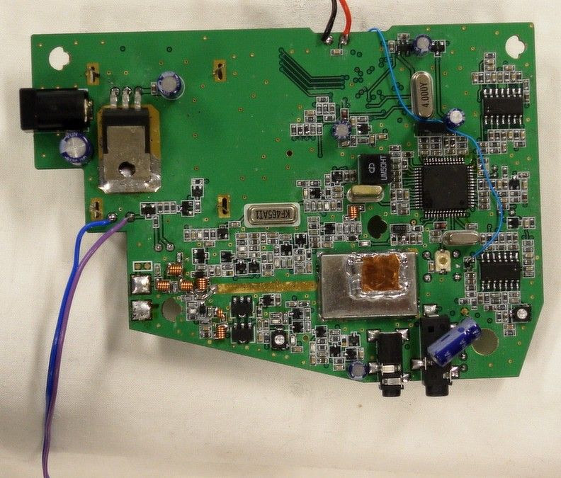
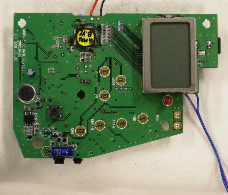
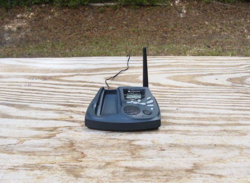
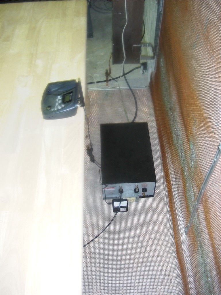
APPLICANT: TTI TECH CO., LTD. FCC ID: PDHGMRS-3000B REPORT #: T/TTI_PDH\508ZKT2\508ZKT2TestReport.doc TABLE OF CONTENTS TABLE OF CONTENTS LIST APPLICANT: TTI TECH CO., LTD. FCC ID: PDHGMRS-3000B TEST REPORT: PAGE 1......COVER SHEET - GENERAL INFORMATION & TECHNICAL DESCR. PAGE 2......TECHNICAL DESCRIPTION CONTINUED PAGE 3......RF POWER OUTPUT PAGE 4......MODULATION CHARACTERISTICS PAGE 5......AUDIO FREQUENCY RESPONSE GRAPH PAGE 6......MODULATION LIMITING GRAPH – 300Hz PAGE 7......MODULATON LIMITING GRAPH – 1000Hz PAGE 8......MODULATION LIMITING GRAPH – 3000Hz PAGE 9......AUDIO LOW PASS FILTER GRAPH PAGE 10.....OCCUPIED BANDWIDTH PAGE 11.....OCCUPIED BANDWIDTH PLOT PAGE 12.....OCCUPIED BANDWIDTH PLOT – CW PAGE 13.....POWER LINE CONDUCTED INTERFERENCE PAGE 14.....POWER LINE PLOT LINE 1 PAGE 15.....POWER LINE PLOT LINE 2 PAGE 16.....SPURIOUS EMISSIONS AT ANTENNA TERMINALS PAGE 17.....UNWANTED RADIATION PAGE 18.....METHOD OF MEASURING RADIATED SPURIOUS EMISSIONS PAGE 19.....FREQUENCY STABILITY PAGE 20-23..LIST OF TEST EQUIPMENT EXHIBITS CONTAINING: EXHIBIT 1.........FCC ID LABEL SAMPLE EXHIBIT 2.........SKETCH OF LOCATION EXHIBIT 3.........EXTERNAL PHOTO – FRONT VIEW EXHIBIT 4.........EXTERNAL PHOTO – TOP VIEW EXHIBIT 5.........INTERNAL PHOTO – CHASSIS VIEW EXHIBIT 6.........INTERNAL PHOTO – COMPONENT VIEW EXHIBIT 7.........INTERNAL PHOTO – COPPER VIEW EXHIBIT 8.........SCHEMATIC EXHIBIT 9.........BLOCK DIAGRAM EXHIBIT 10........USERS MANUAL EXHIBIT 11........CIRCUIT DESCRIPTION EXHIBIT 12........TUNING PROCEDURE EXHIBIT 13-14.....TEST SET UP PHOTO APPLICANT: TTI TECH CO., LTD. FCC ID: PDHGMRS-3000B REPORT #: T\TTI_PDH\508ZKT2\508ZKT2TestReport.doc Page 1 of 23 GENERAL INFORMATION REQUIRED FOR CERTIFICATION 2.1033(c)(1)(2) TTI TECH CO., LTD. will manufacture the FCCID: PDHGMRS-3000B GMRS/FRS COMBINATION TRANSCEIVER in quantity, for use under FCC RULES PART 95. TTI TECH CO., LTD. EUNDO BLDG. # 402, 737-19, BANPO-1DONG SEOCHO-KU, SEOUL, KOREA 137-041 2.1033 (c) TECHNICAL DESCRIPTION 2.1033(c)(3) Instruction book. A draft copy of the instruction manual is included as EXHIBIT 10. 2.1033(c) (4) Type of Emission: 10K5F3E 95.631 Bn = 2M + 2DK M = 3000 D = 1.75K Bn = 2(3000)+2(2250) = 10.5K GMRS Authorized Bandwidth 20.0 kHz 2.1033(c)(5) GMRS Frequency Range: 1. 462.5500 13. 462.7000 95.621 2. 462.5625 14. 462.7125 3. 462.5750 15. 462.7250 4. 462.5875 16. 467.5500 5. 462.6000 17. 467.5750 6. 462.6125 18. 467.6000 7. 462.6250 19. 467.6250 8. 462.6375 20. 467.6500 9. 462.6500 21. 467.6750 10. 462.6625 22. 467.7000 11. 462.6750 23. 467.7250 12. 462.6875 2.10311c)(6)(7) The Maximum Output Power Rating: GMRS – HIGH 1.2 Watts LOW .4 Watts FRS - .4 Watts FRS Authorized Bandwidth 12.5kHz 2.1033(c)(5) FRS Frequency Range: 1. 462.5625 8. 467.5625 95.627 2. 462.5875 9. 467.5875 3. 462.6125 10. 467.6125 4. 462.6375 11. 467.6375 5. 462.6625 12. 467.6625 6. 462.6875 13. 467.6875 7. 462.7125 14. 467.7125 MHz APPLICANT: TTI TECH CO., LTD. FCC ID: PDHGMRS-3000B REPORT #: T\TTI_PDH\508ZKT2\508ZKT2TestReport.doc Page 2 of 23 2.1033(c)(6)(7) Power Output shall not exceed 0.50 Watts effective 95.639 radiated power. There can be no provisions for 95.649 increasing the power or varying the power. 2.1033(c)(8) DC Voltages and Current into Final Amplifier: FINAL AMPLIFIER ONLY GMRS: FOR LOW POWER SETTING INPUT POWER: (9.0V)(.211A) = 1.899 Watts FOR HIGH POWER SETTING INPUT POWER: (9.0V)(.540A) = 4.860 Watts FRS: INPUT POWER: (9.0V)(.214)= 1.926 Watts 2.1033(c)(9) Tune-up procedure. The tune-up procedure is included as EXHIBIT # 12. 2.1033(c)(10) Complete Circuit Diagrams: The circuit diagram is included as EXHIBIT 8 of this report. The block diagrams are included as EXHIBIT 9 of this report. 2.1033(c)(11) A photograph or a drawing of the equipment identification label is included as exhibit No. 1. 2.1033(c)(12) Photographs(8"X10") of the equipment of sufficient clarity to reveal equipment construction and layout, including meters, labels for controls, including any view under shields. See exhibits 3-7. 2.1033(c)(13) Digital modulation is not allowed. 2.1033(c)(14) The data required by 2.1046 through 2.1057 is submitted below. APPLICANT: TTI TECH CO., LTD. FCC ID: PDHGMRS-3000B REPORT #: T\TTI_PDH\508ZKT2\508ZKT2TestReport.doc Page 3 of 23 95.639 Power Output shall not exceed 50.0 Watts effective radiated power. There can be no provisions for 95.649 increasing the power or varying the power. 2.1046(a) RF power is measured by the substitution method as outlined in TIA/EIA - 603. With a nominal battery voltage of 6.0 V, and the transmitter properly adjusted the RF output measures: OUTPUT POWER: GMRS: HIGH 1.2 Watts ERP LOW .4 Watts ERP FRS: .4 Watts ERP 2.1046(a) RF power output. The test procedure used was TIA/EIA-603 S2 APPLICANT: TTI TECH CO., LTD. FCC ID: PDHGMRS-3000B REPORT #: T\TTI_PDH\508ZKT2\508ZKT2TestReport.doc Page 4 of 23 2.1047(a)(b) Modulation characteristics: AUDIO FREQUENCY RESPONSE The audio frequency response was measured in ac- cordance with TIA/EIA Specification 603. The audio frequency response curve is shown on the next page. The audio signal was fed into a dummy microphone circuit and into the microphone connector. The input required to produce 30 percent modulation level was measured. See Page 5 of report. 2.1047(b) Audio input versus modulation The audio input level needed for a particular per- percentage of modulation was measured in accor- dance with TIA/EIA Specification 603. The audio input curves versus modulation are on the following pages. Curves are provided for audio input frequen- cies of 300, 1000, and 3000 Hz. See Pages 6,7 & 8 of report. 95.637 Post Limiter Filter Each GMRS transmitter, except a mobile station transmitter with a power of 2.5Watts or less, must be equipped with an audio low pass filter. At any frequency between 3 & 20 kHz the filter must have an attenuation of 60log (f/3) greater than the attenuation at 1KHz. See Page 9 of report. APPLICANT: TTI TECH CO., LTD. FCC ID: PDHG…
Text truncated - open the document above for the full version.
Contact Information
Applicant
J. N. LEE(Manager)
Technical Contact
Timco Engineering, Inc.Mario R de Aranzeta
[email protected]888-472-2424
849 NW State Road 45 · Newberry, Florida · United States
Non-Technical Contact
Timco Engineering, Inc.Sharon A Hoffman
[email protected]888-472-2424
Test Firm
Timco Engineering, Inc.S Sanders
Technical Specifications
| # | Rule Parts | Frequency Range | Power Output | Emission | Tolerance |
|---|---|---|---|---|---|
| 4 | 95B | 467.5625 MHz - 467.7125 MHz | 400.00 mW | 10K5F3E | 2.5 ppm |
Other Applications from TTI Tech Co., Ltd.
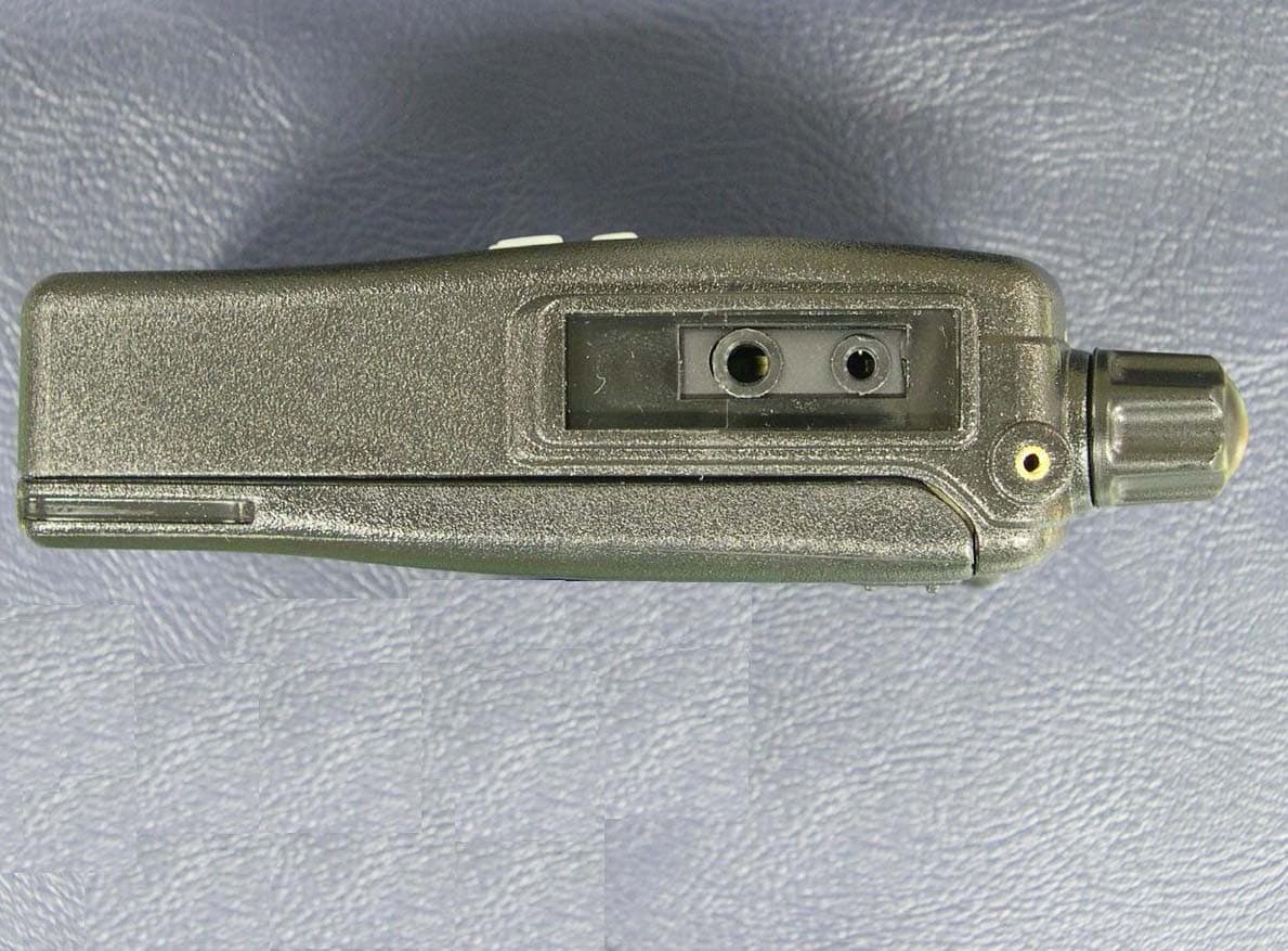
PDHTX150M
Jan 18, 2007HANDHELD MARINE RADIO
Equipment Class
TNF - Licensed Non-Broadcast Transmitter Held to Face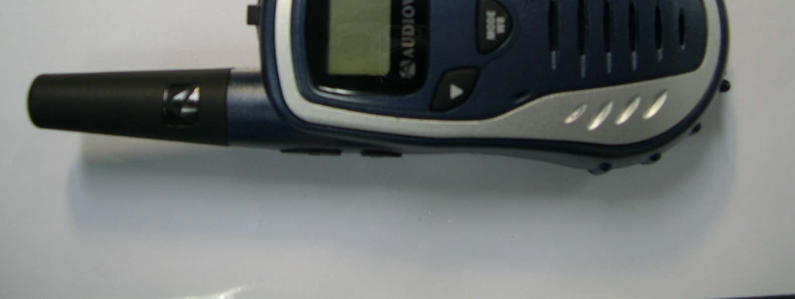
PDHGMRS200
Jul 05, 2005FRS/GMRS COMBINATION
Equipment Class
FRF - Part 95 Family Radio Face Held Transmitter
PDHGMRS1202
Feb 06, 2005FRS/ GMRS Combination
Equipment Class
FRF - Part 95 Family Radio Face Held Transmitter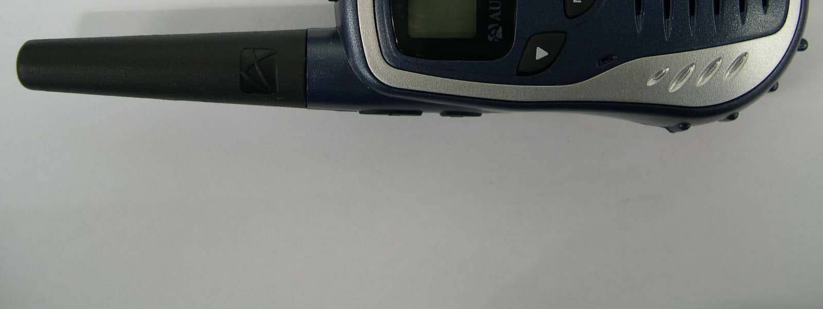
PDHGMRS602
Feb 06, 2005FRS/ GMRS Combination
Equipment Class
FRF - Part 95 Family Radio Face Held Transmitter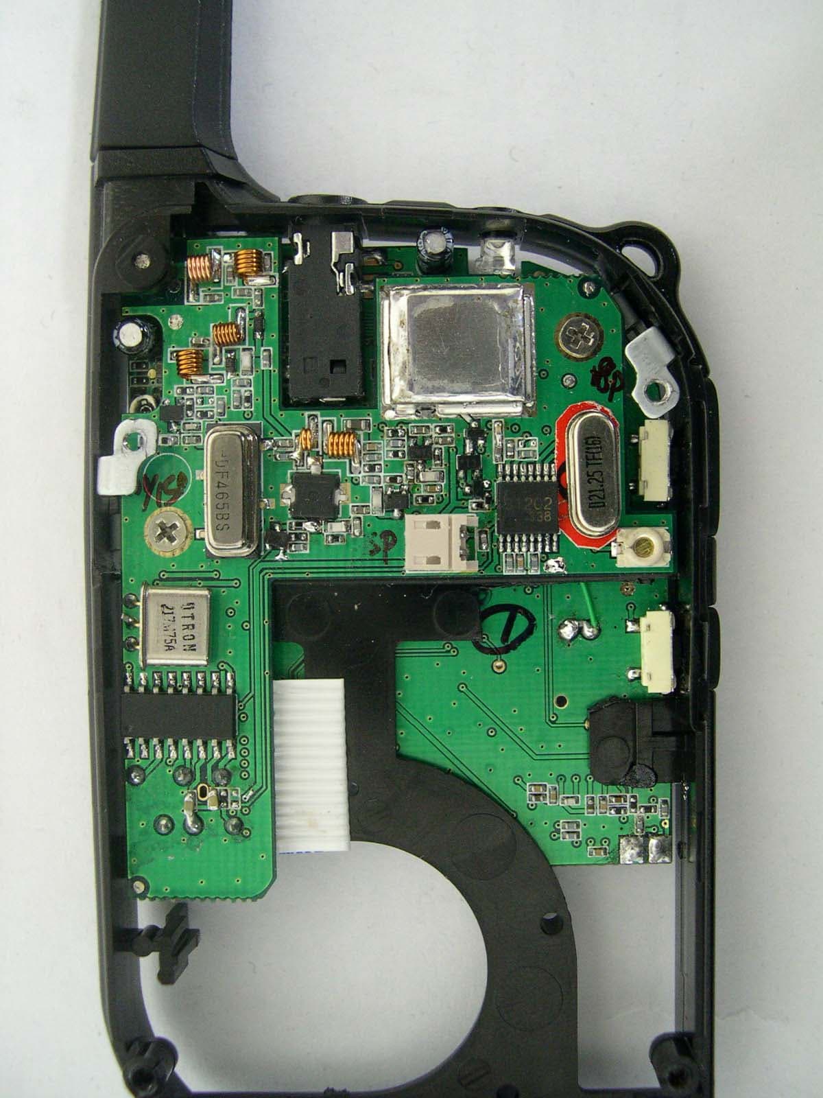
PDHGMRS500SLK
Apr 06, 2004GMRS/FRS Combination
Equipment Class
FRF - Part 95 Family Radio Face Held Transmitter