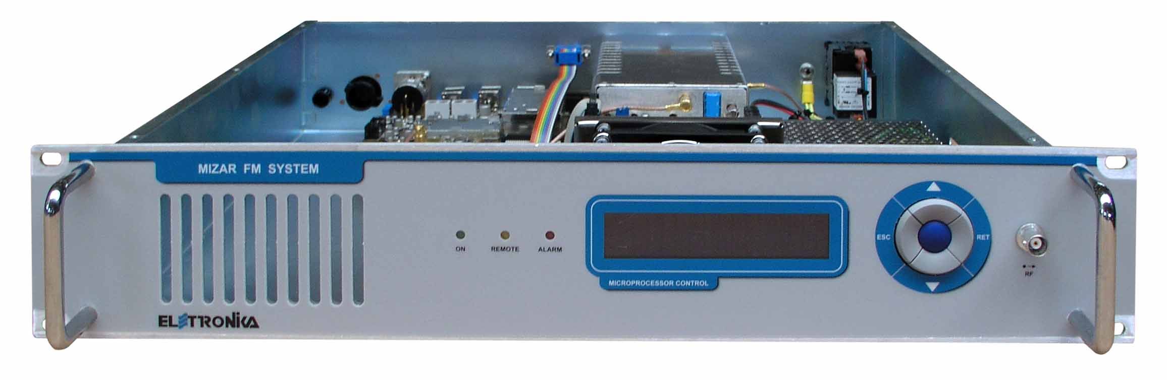
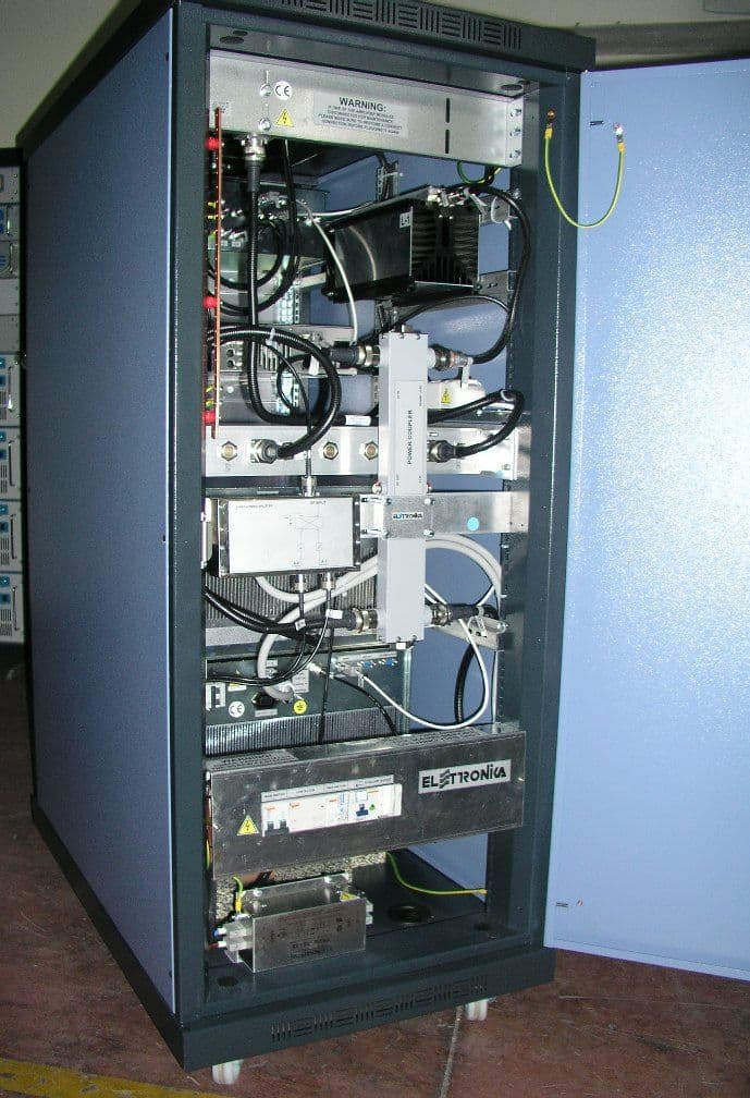
PHLMIZAR3030 Watt FM Broadcast Transmitter
Elettronika S.r.l.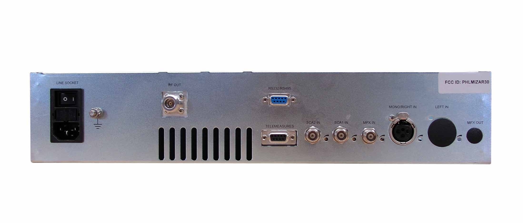
Click to zoom
Application Details
- Equipment Class
- TBC - Licensed Broadcast Station Transmitter
- Date of Grant
- Jul 01, 2008
- Application Purpose
- Original Equipment
- Date of Application
- Mar 18, 2008
- Equipment Note
- 30 Watt FM Broadcast Transmitter
- Frequency Range
- 87.90000000 - 108.00000000
- Company
- Elettronika S.r.l.
- Country
- Italy
Documents & Files

Document Text
Text extracted from the exhibit documents filed with the FCC. Open a document above to read the original.
Users Manual
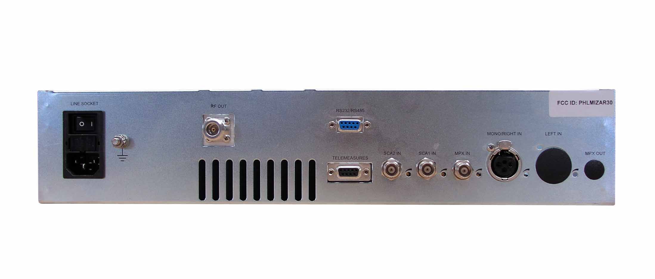
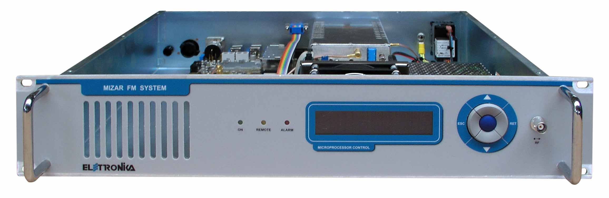
MIZAR FM Transmitter System CODEAPF073A APF074A TITLEMIZAR FM TRANSMITTERREV 1.1DATE26/07/07 30W300W MONO APF073A MIZAR30 APF074A MIZAR300 STEREO APF073A+OPT023 MIZAR30S APF074A+OPT023 MIZAR300S MIZAR Transmitter Family SS 96 Km 113 70027 Palo del Colle (Ba) ITALY Tel. +39 (0)80 626755 Fax +39 (0)80 629262 E-mail: [email protected] Web site: http://www.elettronika.it Registration number: IT-17686 Registration number: IT-24436 POWER AUDIO Mizar Transmitter Family .................................................................................................. 2 Summaries ......................................................................................................................... 3 Warning .............................................................................................................................. 7 Warranty............................................................................................................................. 8 Introduction....................................................................................................................... 9 Content of the manual ...................................................................................................... 9 Treatment of electrical shock ......................................................................................... 11 First-aid......................................................................................................................... 12 Treatment of electrical burns......................................................................................... 12 Note ............................................................................................................................... 12 RoHS Normative.............................................................................................................. 13 MIZAR FM Transmitter System ....................................................................................... 15 Section 1 - Information ................................................................................................... 17 1.1 Description.............................................................................................................. 18 1.2 Technical characteristcs .......................................................................................... 19 1.3 Front panels ............................................................................................................21 1.4 Rear panels .............................................................................................................22 Block Diagram...............................................................................................................23 Section 2 - Installation .................................................................................................... 25 2.1 Operating environment............................................................................................ 26 2.2 First installation....................................................................................................... 26 2.3 Installation of MIZAR Mono with external Stereo Coder .......................................... 27 2.4 Installation of MIZAR Stereo with external RDS Coder ........................................... 27 2.5 MIZAR remote control with Elettronika RCU ........................................................... 28 Section 3 - Operation ...................................................................................................... 29 3.1 User interface and software settings ....................................................................... 30 3.2 AGC Implementation............................................................................................... 32 3.3 Alarms and automatic behaviours........................................................................... 33 3.4 Status LEDs ............................................................................................................33 Section 4 - Diagram ......................................................................................................... 35 - APF073A MIZAR30 Cable Diagram ............................................................................ 36 - APF074A MIZAR300 Cable Diagram .......................................................................... 37 - APF073A_APF074A MIZAR Component list ............................................................... 38 - SCH0377A Mother Board............................................................................................ 39 - Description .............................................................................................................. 39 - SCH0377A Component layout ................................................................................ 40 - Calibration procedure .............................................................................................. 41 - Instrument list ...................................................................................................... 41 Summaries - Description of the adjustment points................................................................... 41 - Component layout for adjustment points ............................................................. 42 - RF Section .......................................................................................................... 43 - Modulation Section .............................................................................................. 43 - Audio Section ...................................................................................................... 43 - General ............................................................................................................... 43 - SCH0377A Component list ..................................................................................... 44 - SCH0377A Electric Diagram .........…
Text truncated - open the document above for the full version.
Attestation Statements
March 19, 2008 FCC Office of Equipment Authorization To Whom It May Concern: ATTESTATION STATEMENT I hereby certify the measurements and test results were made and recorded in accordance with accepted engineering practices and do constitute an accurate representation of the product performance of the documented MIZAR 30 transmitter. Signed, President
Operational Description
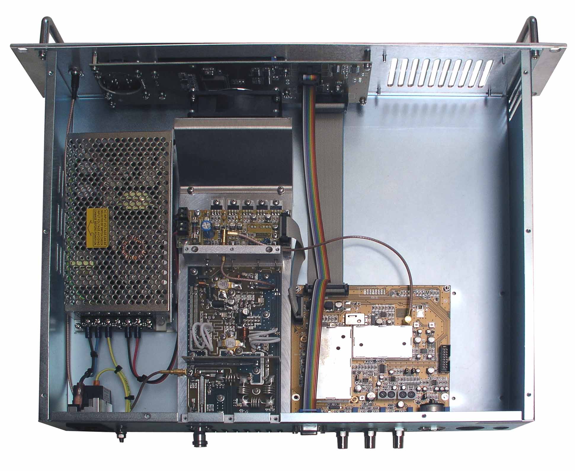
March 22, 2008 THEORY OF OPERATION—MIZAR 30 The overall theory of operation for the MIZAR30 is provided on this page. Detailed theory of operation is outlined in the technical manual for each major sub-assembly (synthesizer, power amplifier, etc.) The audio signals comprised of left and/or right channel audio, and any subcarrier generator audio are fed to the mother board and the coder board. These two boards contain the necessary pre-emphasis and stereo encoding as required for the audio signal employed. The composite audio signal is then fed to a limiter to prevent overmodulation and sent to the voltage controlled oscillator (VCO). The VCO creates a linear FM waveform on the actual RF channel to be transmitted as programmed by the synthesizer. The synthesizer generates the proper frequency for the designated frequency channel and it uses a temperature compensated crystal controlled oscillator to control the carrier frequency to the prescribed FCC frequency tolerance. Once on the correct frequency, the RF driver amplifies the RF signal to a level that can drive the RF power amp. The RF power amp receives the RF signal from the driver and amplifies the signal to 30 watts. At the output of the RF PA, a filter is employed to prevent harmonics from reaching the output connector. Each one of the subassemblies mentioned in this paragraph uses a DC voltage. The DC voltages are generated by the switching power supply that receives its control signal from the controller assembly. The controller assembly provides a user interface and sends the appropriate voltages to the various subassemblies to program the correct mode of operation, the frequency of operation, the output power level, engages the cooling fan, etc. The controller also monitors specific parameters of the subassemblies and displays that information as selected from the front panel. Greg Best Consulting, Inc. 9223 N. Manning Ave. Kansas City, MO 64157 816-792-2913
Parts List/Tune Up Info
38 Part Name CodeDescriptionQty 02035BNC CONNECTOR FOR RG316 CABLE1 0251390 SMB SOCKET cod. R114186000W2 (APF073A)1 (APF074A) 02518SMB SOCKET FOR RG174 CABLE code R114082000W 1 (APF073A)2 (APF074A) 02695DB9 CONNECTOR FOR IU008059 CABLE1 02699FEMALE 10WIRE CONNECTOR1 02700FEMALE 16WIRE CONNECTOR2 02833AC SOCKET WITH FUSE-HOLDER1 (APF074A) 028413 POLES CANON PLUG1 02855FEMALE 26WIRE CONNECOTR2 05069TOROIDAL FILTER1 (APF074A) 05551B2U HANDLE KIT2 (APF073A) 05552B3U HANDLE KIT2 (APF074A) 07522LIGHTED SWITCH1 (APF073A) 07524ABLACK SWITCH1 (APF074A) 07602BLOWER GRID1 (APF073A)2 (APF074A) 07613PAPST BLOWER1 (APF073A)2 (APF074A) 07918AC FILTER1 (APF073A) 07924PVC PROTECTION1 (APF074A) 07925PVC PROTECTION1 07926PVC PROTECTION1 (APF073A) 08502RG 316 50Ω CABLE0.70 (APF073A)0.90 (APF074A) CON0306CON0306R0 COVER1 CON0340SCON0340R1S MIZAR30 BOX1 (APF073A) CON0354R2SCON0354R2 MIZAR300 BOX1 (APF074A) DET1220DET1220R1 BLOWER CONVEYER1 (APF073A) DET1317R0PDET1317R0P MECHANICAL DETAIL1 (APF074A) DET1361R0PDET1361R0 MECHANICAL DETAIL1 (APF074A) E0050PSP-650-48 DE2 SWITHCING POWER SUPPLY1 (APF074A) E0060S-100F-24 SWITCHING POWER SUPPLY1 (APF073A) FUS5A5A FUSE2 (APF073A) FUS10B10A FUSE2 (APF074A) MFF0025BR030W FM AMPLIFIER MODULE1 (APF073A) MFF0031AR0300W FM AMPLIFIER MODULE1 (APF074A) PAN0141PAN0141R1 FRONT PANEL1 (APF073A) PAN0153R0PFRONT PANEL1 (APF074A) SCH0372AR1DISPLAY BOARD1 SCH0377AR2MOTHER BOARD1 V0761BLACK PLASTIC TAP1 V0768BLACK PLASTIC TAP1 Component listAPF073A_APF074A - MIZAR 44 SCH0377AR2 COMPONENT LIST Part Name/NumberDescriptionQty.Comps.Page 1/2 257BLR-3618N 0501005010 AUDIO TOKO FILTER2LP1-2 CC 100nF-S 01065C01065C Y5V 1206 CAPACITOR20C19, C30, C32, C43, C45-46, C57, C62-63, C77, C79, C81-89 CC 10pF-S 0108601086 SMD 1206 CAPACITOR1C26 CC 1206 N. M.N. M. SMD 1206 CAPACITOR1C58 CC 1nF-2%-S 01041D01041D SMD 1206 CAPACITOR23C9-10, C22, C25, C34-36, C49-50, C54, C56, C59-61, C64-65, C68-72, C75, C80 CC 27pF-S 01022B01022B SMD 1206 CAPACITOR16C1-6, C11-14, C28-29, C33, C37, C51-52 CC 6p8F-S 0108401084 SMD 1206 CAPACITOR1C39 CE 100uF16V-S 01792A01792A ELET. SMD CAPACITOR 3C78, C91-92 CE 10uF16V-S 01776A01776A ELET. SMD CAPACITOR 14C7, C16-18, C20, C41-42, C47-48, C53, C55, C73-74, C76 CE 220uF16V-S01824A ELET. SMD CAPACITOR 5C8, C27, C40, C66-67 CE 22uF16V-S01780A ELET. SMD CAPACITOR 6C21, C23-24, C31, C38, C44 CE 470uF-S 16V-S01804B ELET. SMD CAPACITOR 1C15 D BAS85-S03024 SMD DIODE SCHOTTKY1D2 D BAT54S03199 SMD SCHOT. DIODE A-K T 3D1, D4-5 D HSMP381403202 SMD DIODE1D3 DL KA-3528SGC 0305703057 GREEN SMD LED DIODE1DL1 DZ 5V1-S 0312803128 SMD ZENER DIODE2DZ1-2 IC LM833-S 04643A04643A SMD INTEG CIRCUIT3IC1-3 IC LMC6482-S04632 SMD INTEG CIRCUIT2IC5, IC8 IC LMC6484-S04634 SMD INTEG CIRCUIT1IC7 IC MAR3 0436704367 SMD INTEG CIRCUIT1IC6 IC MC14066BD-S 4708B4708B SMD INTEG CIRCUIT1IC4 IND 100nH-S 05093A05093A INDUCTOR1L9 IND 22uH-S 5023D5023D INDUCTOR5L1-3, L5-6 IND 2u2H-S 05020A05020A INDUCTOR1L7 IND CBD8 0507205072 INDUCTOR3L4, L8, L10 IND MS85 10uH-S04948 INDUCTOR 2.7A2L12-13 J BNC-90G-PCB SHIELD02034A PCB SHIELDED CONNEC. 3J2-4 J DB9-90G 0279702797 PCB CONNECTOR1J5 J FC-16P 02701-0270002701+02700 PCB CONNECTOR2J7, J10 J FC-26P 02855-0285402855+02854 PCB CONNECTOR1J12 J NC3FD-H 0286202862 XLR-90G-PCB SOCKET F.1J1 J SMB-PCB 2PIN 0251602516 PCB CONNECTOR3J6, J8-9 JU JUMP2 02739-0274202739+02742 MASCHIO PAN24JP1-4 OSC NVT535 0516805168 TCXO1OSC1 PN0658A SCH0007AR0SCH0007AR0 VCO FM INTEG.1VCO1 R 0R0-S 0000100001 RES 1/4W 5% SMD 12061R98 R 100K-1%-S 00065B00065B RES 1/4W 1% SMD 120612R33-34, R37, R41, R48, R50, R55, R57, R62, R88, R91, R96 45 Part Name/NumberDescriptionQty.Comps.Page 2/2 R 100R-S 00029A00029A RES 1/4W 5% SMD 120612R5-7, R10, R38, R71, R76, R82, R86-87, R92, R97 R 10K-S 00053A00053A RES 1/4W 5% SMD 120617R8-9, R11, R22, R29-30, R40, R45-46, R52, R53, R60, R66, R73, R100-101, R107 R 10R-S 00017A00017A RES 1/4W 5% SMD 12062R64, R69 R 15K-1%-S 00055B00055B RES 1/4W 1% SMD 12063R35, R85, R94 R 1K2-1%-S 00042A00042A RES 1/4W 1% SMD 12065R19-20, R44, R67, R79 R 1K5-S 00043A00043A RES 1/4W 5% SMD 12061R68 R 22K-S 00057A00057A RES 1/4W 5% SMD 12064R17, R43, R89-90 R 2K2-S 00045A00045A RES 1/4W 5% SMD 12062R61, R70 R 330R-1%-S 00035A00035A RES 1/4W 1% SMD 12061R75 R 47K-1%-S 00061B00061B RES 1/4W 1% SMD 120618R18, R26-28, R32, R42, R49, R51, R54, R56, R58-59, R63, R65, R93, R95, R102, R108 R 4K7-S 00049A00049A RES 1/4W 5% SMD 12066R15, R23-25, R36, R39 R 560K-S00074B RES 1/4W 5% SMD 12061R31 R 560R-1%-S 00038B00038B RES 1/4W 1% SMD 12061R74 R 68K-1%-S 00063B00063B RES 1/4W 1% SMD 12065R12-14, R16, R47 R 68R-S 00027A00027A RES 1/4W 5% SMD 12062R77-78 R 82R-S 00028A00028A RES 1/4W 5% SMD 12061R72 RV 10K-M-H 0077700777 VARIABLE RESISTOR4R1-4 RV 10K-S-H/S 0079300793 SMD VARIABLE RESISTOR 2R80-81 RV 1K-S-H/S 0079200792 SMD VARIABLE RESISTOR 1R21 RV 50K-S-H/S 0079700797 SMD VARIABLE RESISTOR 2R83-84 TR BC807 0345303453 PNP SMD TRANSISTOR1TR6 TR BC848 0345703457 NPN SMD TRANSISTOR7TR1-2, TR4-5, TR8-9, TR12 TR BC856 0345503455 PNP SMD TRANSISTOR1TR3 TR BFG35 0399003990 NPN SMD TRANSISTOR1TR7 50 SCH0378AR2 COMPONENT LIST Part Name/NumberDescriptionQty.Comps. 257BLR-3618N 0501005010 AUDIO TOKO FILTER2LP1-2 CC 100nF-S 01065C01065C Y5V 1206 CAPACITOR6C14, C22, C24, C30, C33, C37 CC 1nF-2%-S 01041D01041D SMD 1206 CAPACITOR5C13, C16-18, C23 CC 27pF-S 01022B01022B SMD 1206 CAPACITOR9C4, C6-8, C10-11, C15, C20, C32 CE 10uF16V-S 01776A01776A ELET. SMD CAPACITOR 7C2-3, C5, C9, C19, C34-35 CE 22uF16V-S01780A ELET. SMD CAPACITOR 6C12, C21, C25-27, C31 CE 470uF-S 16V-S01804B ELET. SMD CAPACITOR 5C1, C29, C38-40 CV 4.5-20pF-S 0148101481 VARIABLE CAPACITOR1C28 CV 7-50pF-S 0147401474 VARIABLE CAPACITOR1C36 D BAT54S03199 SMD SCHOT. DIODE A-K T 1D1 IC LM833-S 04643A04643A SMD INTEG CIRCUIT2IC1-2 IC LMC6482-S04632 SMD INTEG CIRCUIT1IC4 IC MC14066BD-S 4708B4708B SMD INTEG CIRCUIT1IC3 IND 22uH-S 5023D5023D INDUCTOR2L1-2 J BNC-90G-PCB SHIELD02034A PCB SHIELDED CONNEC. 1J1 J FC-16P 02701-0270002701+02700 PCB CONNECTOR1J4 J NC3FD-H …
Text truncated - open the document above for the full version.
Schematics
23 Block diagram MONO / RIGHT MPX IN SCA1 SOCKET 50 s LOW PASS FILTER LIMITER VCO LEVEL PLL SCA2 SOCKET LEFT 50 s LOW PASS FILTER CODER MP X OUT LEFT RIGHT RF DRIVER INTERFACE BOARD REF FWD GATE MONITOR RF OUT BLOWER 27V AC/DC FILTER VA C RS232 / RS485 SOCKET TELEMEASURES SOCKET TCXO AC SOCKET MOTHER BOARD DISPLAY BOARD CODER BOARD 36 37 46 51 54 61 62 72 73 74 76 81 ACTIVE INRUSH CURRENT LIMITING EMI FILTER I/P FG RECTIFIERS & P. F. C . POWER SWITCHING O.L.P. PWM CONTROL RECTIFIERS & FILTER O.C.P. O.V.P. O.T.P. DETECTION CIRCUIT FAN SIGNAL CONTROL CURRENT SHARING CIRCUIT PFC fosc: 88kHz PWM fosc: 100kHz POK P +V -V RC.G. RC BLOCK DIAGRAM DERATING CURVE AMBIENT TEMPERATURE ( C) o LOAD ( % ) -200102030455060 (HORIZONTAL) 20 40 50 60 80 100 INPUT VOLTAGE (V) 60Hz 11 588100135155230264 90 100 80 70 60 50 40 LOAD(%) OUTPUT DERATING VS INPUT VOLTAGE 83 85
Test Report
TEST REPORT ELETTRONIKA S.r.l FM TRANSMITTER TECHNICAL REPORT INTRODUCTION The following information is provided to verify the technical performance of the MIZAR 30 FM transmitter. The following information is supplied for FM broadcast service according to applicable portions of Part 2 and Part 73 of the FCC rules and regulations 1. Power Output Measurements as indicated by FCC Rule Part 2.1046 and 73.267. 2. Frequency stability measurements associated with variations in ambient temperature and with variations in line voltage as specified by 73.1545. 3. Occupied BW of the FM signal as specified by FCC Rule Part 73.297, 73.317, 73.322, and 73.1570. 4. Measurement of conducted harmonics and spurs outside its assigned channel as specified by FCC Rule Part 73.317. 5. Demodulated Amplitude versus Frequency response measurements of the transmitter compliant with the Engineering charts identified in 73.333. 6. Measurement of cabinet radiation of spurs and harmonics as specified in FCC Rule 2.1053 and 2.1057. 7. Measurements of voltage and current to final amp stage as outlined in FCC Rule 2.1033. Measurements were conducted at power output levels of 30 watts and 7.5 watts and constitute the range of power for which type certification is sought. FIGURE 1--TEST EQUIPMENT CONFIGURATION The test equipment used for the measurements is listed at the back of this exhibit. All test equipment had been calibrated prior to the use of the equipment by the supplier of the test equipment. RF Power Output Stability vs Line Voltage The equipment was configured as shown in Figure 1. The loss through the RF output cable and directional coupler and attenuator was calibrated at the carrier frequency of 98 MHz. The audio generator was not energized. The transmitter was energized at room temperature at an initial power output of 30 watts. Power was read on the Bird 4391A Power Meter and a reference level was established on the Advantest R131 Spectrum Analyzer. The line voltage was varied from 94 volts to 126 volts using a variac to adjust the voltage. The test was repeated at an output power of 7.5 watts. The data is tabulated on the next page. Audio Generator (Part of Modulation Analyzer) MIZAR 30 Directional Coupler Power Meter Modulation Analyzer Spectrum Analyzer Audio Voltage Measurement RF Load RF Power Power Supply RF Power Power Supply 30W 94V ac 7.5W 94V ac 30W 110V ac 7.5W 110V ac 30W 126V ac 7.5W 126V ac RF Power Output Stability vs Temperature The equipment was configured as shown in Figure 1. The loss through the RF output cable and directional coupler and attenuator was calibrated at the carrier frequency of 98 MHz. The audio generator was not energized. The transmitter was energized at room temperature at a power output of 30 watts. Power was read on the Bird 4391A Power Meter and a reference level was established on the Advantest R131 Spectrum Analyzer. Next the temperature was varied from 0 C to +50 C. Data at the extreme temperature limits and at room temperature was recorded regarding power output. The transmitter was adjusted to 7.5 watts and the procedure was repeated. FRQUENCY STABILITY The equipment was configured as shown in Figure 1. The loss through the RF output cable and directional coupler and attenuator was calibrated at the carrier frequency of 98 MHz. The audio generator was not energized. The transmitter was energized at room temperature at a power output of 30 watts. Power was read on the Bird 4391A Power Meter and a reference level was established on the Advantest R131 Spectrum Analyzer. The line voltage was varied from 94 volts to 126 volts. The output frequency was read on the spectrum analyzer with the counter mode engaged. The results are tabulated below. RF Frequency Power Supply 97,9999995MHz 94V ac 98,0000000MHz 110V ac 98,0000006MHz 126V ac CONDUCTED EMISSION Two configurations have been considered: Monophonic and Stereophonic. MONO (15KHZ TONE MODULATING THE CARRIER 85% - DEVIATION 63.75KHZ) Markers at 120kHz from the carrier. Below 25dBc => Pass RF Power Temperature RF Power Temperature 31.5W 0°C 7.8W 0°C 30 W 25°C 7.5W 25°C 27.2 W 50°C 6.8W 50°C 3 Markers at 240kHz from the carrier. Below 35dBc => Pass Markers at 600kHz from the carrier. Below (43+10logP)= 58 dBc => Pass 4 STEREO 15 KHz MAIN SUBCHANNEL AT 38% MODULATION (28.5 KHz DEVIATION), 15KHz STEREO SUBCHANNEL AT 38% MODULATION (28.5 KHz DEVIATION), PILOT TONE AT 9% MODULATION (6.75 KHz DEVIATION) Markers at 120kHz from the carrier. Below 25dBc => Pass Markers at 240kHz from the carrier. Below 35dBc => Pass Markers at 600kHz from the carrier. Below (43+10logP)= 58 dBc => Pass 5 Marker more than 10MHz from the carrier. Below (43+10logP)=58dBc => Pass As can be seen in the above graphs, in the mono and stereophonic modes, the emissions meet the requirements as outlined in FCC Rule 73.317. The rule stipulates emissions between 120 kHz and 240 kHz from the carrier frequency are -25 dB or better, emissions between 240 kHz and 600 kHz from the carrier are -35 dB or better, and emissions greater than 600 kHz from the carrier are at least 43 + 10 log P o , or -58 dB referenced to the unmodulated carrier (top of the screen for these graphs). PILOT FREQUENCY AND 38 kHz LEVEL The frequency of the pilot tone was measured to be 19.000 kHz. Its deviation was set at 7.5 kHz, using the FMAB. The deviation of the subcarrier of the pilot tone (38kHz) must be no more than 0.75kHz. This is measured by means of the FMAB, and confirmed by using the spectrum analyzer in order to display the subcarrier level. The photo below demonstrates the frequency to be 37.98 kHz and the amplitude is 43.5 dB relative to the pilot frequency. 6 CONDUCTED HARMONICS Conducted harmonics are sampled in the output transmission line and converted to the corrected value (using the directional coupler coupling value and cable loss) and then compared to the power output of the unit under test. The correction factor and measured level are used to find the actual l…
Text truncated - open the document above for the full version.
Test Report
MIZAR 30 SUPPLEMENTAL TEST DATA FREQUENCY STABILITY VS TEMPERATURE PERFORMANCE The equipment was configured as shown in Figure 1 of the test report block diagram with the transmitter enclosed within a temperature chamber. The loss through the RF output cable and directional coupler was calibrated at the carrier frequencies of 98 MHz. The audio generator was not energized. The transmitter was energized at room temperature at a power output of 30 watts. Power was read on the Bird 4391A Power Meter and a reference level was established on the Advantest R131 Spectrum Analyzer. The temperature was then varied from +50 °C to 0 °C per FCC rule 2.1055 (a) (3) and the frequency was measured with spectrum analyzer. The temperature was allowed to stabilize at each one of the measurement points. The output frequency was read on the spectrum analyzer with the counter mode engaged. The results meet the FCC tolerance requirements outlined in 73.1545 and are tabulated below. Temperature Frequency [°C] [MHz] 0 98.000010 10 98.000005 20 98.000000 30 97.999996 40 97.999992 50 97.999986
Contact Information
Applicant
Francesco Paparella(Design Omologation and Compliance Mgr)
Technical Contact
Greg Best Consulting, Inc.Gregory L. Best
[email protected]816-792-2913
9223 N. Manning Avenue · Kansas City, Missouri · United States
Technical Specifications
| # | Rule Parts | Frequency Range | Power Output | Emission | Tolerance |
|---|---|---|---|---|---|
| 1 | 73,74 | 87.9 MHz - 108 MHz | 30 W | 300KF8E | 1000.0000000000 Hz |
Other Applications from Elettronika S.r.l.
PHLTXUD1000A
Jul 07, 20101000 W ATSC Transmitter
Equipment Class
TBC - Licensed Broadcast Station Transmitter
PHLTXUD3000A
Jun 17, 20103000 Watt ATSC Transmitter
Equipment Class
TBC - Licensed Broadcast Station Transmitter
PHLTXUD2000A
Jun 09, 20102000 Watt ATSC Transmitter
Equipment Class
TBC - Licensed Broadcast Station Transmitter
PHLMIZAR300
Jul 01, 2008300 Watt FM Broadcast Transmitter
Equipment Class
TBC - Licensed Broadcast Station Transmitter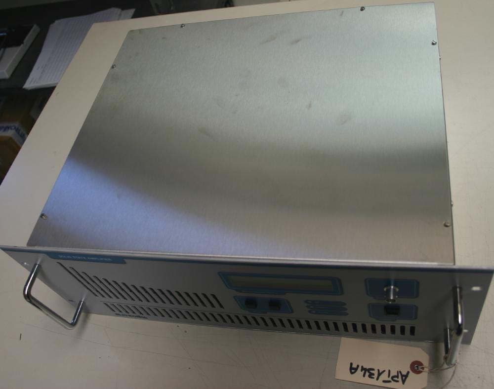
PHLTXUP200
May 29, 2007250 Watt Analog TV Broadcast Transmitter
Equipment Class
TBC - Licensed Broadcast Station Transmitter