PHLTXUP200250 Watt Analog TV Broadcast Transmitter
Elettronika S.r.l.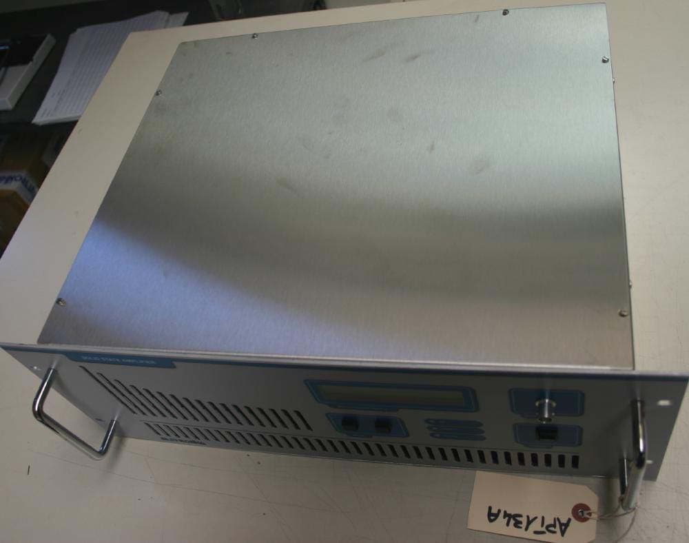
Click to zoom
Application Details
- Equipment Class
- TBC - Licensed Broadcast Station Transmitter
- Date of Grant
- May 29, 2007
- Application Purpose
- Original Equipment
- Date of Application
- Feb 05, 2007
- Equipment Note
- 250 Watt Analog TV Broadcast Transmitter
- Frequency Range
- 614.00000000 - 806.00000000
- Company
- Elettronika S.r.l.
- Country
- Italy
Documents & Files
Document Text
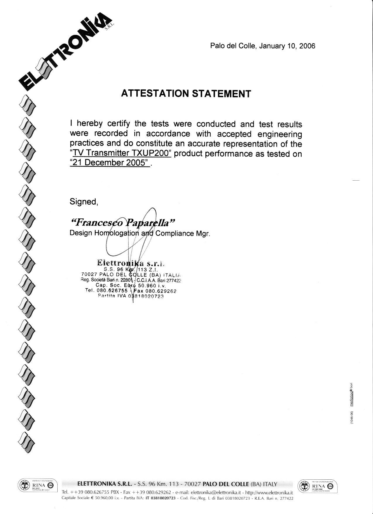
Text extracted from the exhibit documents filed with the FCC. Open a document above to read the original.
Users Manual
AUTV/250LD LDMOS - UHF TV Solid State Amplifier CODEAPT134ATITLEAUTV/250LDREV 0DATE06/11/03 SS 96 Km 113 70027 Palo del Colle (Ba) ITALY Tel. +39 (0)80 626755 Fax +39 (0)80 629262 E-mail: [email protected] Web site: http://www.elettronika.it Registration number: IT-17686 Registration number: IT-24436 3 WARNING The apparatus described in this manual has been designed and manufactured with devices to safe- guard the users. In any case it is recommended that during any operation of installation, maintenance, miscellaneous interventions and calibrations requiring the apparatus to be switched on, THE USER TAKES ALL THE PRECAUTIONS AGAINST INCIDENTS It is required to use the proper clothes and protection gloves in order to prevent damages from inci- dental contacts with high-voltage parts. The manufacturer declines every responsibility in case the recommendations above are not followed. IMPORTANT The component lists attached to the relevant electrical diagrams indicate for each item the reference, the description and the type normally used. The Elettronika S.r.l. though reserves the right to use or supply as spare parts components with equivalent characteristics but of a different type, assuring anyway the optimal work of the apparatus in accordance with the specifications. The enclosed monographs are solely owned by Elettronika S.r.l. The use of anything enclosed in this technical manual without explicit authorization given by Elettronika S.r.l. will be prosecuted by the law. The data and technical characteristics of the apparatus described in this manual are not compelling for the manufacturer. The Elettronika S.r.l. reserves the right to make, without previous notice, modifications or updates in order to improve the quality of the product. The general conditions of supply and sale are described in the contracts. The delivery time are in accordance with the products and quantities ordered. 4 Summary of warranty We, ELETTRONIKA S.r.l., SS096 Km 113 Z.I. PALO DEL COLLE (BA) ITALY, warrant to the ORIGINAL PURCHASER of a NEW product, for a period of one (1) year from the date of purchase by the original purchaser (the “warranty period”) that the new ELETTRONIKA product is free of defects in materials and workmanship and will meet or exceed all advertised specifications for such a product. This warranty does not extend to any subsequent purchaser or user, and automatically terminates upon sale or other disposition of our product. Items excluded from this ELETTRONIKA warranty We are not responsible for product failure caused by misuse, accident, or neglect. This warranty does not extend to any product on which the serial number has been defaced, altered, or removed. It does not cover damage to loads or any other products or accessories resulting from ELETTRONIKA product failure. It does not cover defects or damage caused by use of unauthorized modificstions, accessories, parts, or service. What we will do We will remedy any defect, in material or workmanship (except as excluded), in our sole discretion, by repair, replacement, or refund. If a refund is elected, then you must make the defective or malfunctioning component available to us free and clear of all liens or other encumbrances. The refund will be equal to the actual purchase price, not including interest, insurance, closing costs, and other finance charges less a reasonable depreciation on the product from the date of original purchase. Warranty work can only be performed at our authorized service centers or at our factory. Expenses in remedying the defect will be borne by ELETTRONIKA, including one-way surface freight shipping costs within the United States. (Purchaser must bear the expense of shipping the product between any foreign country and the port of entry in the United States and all taxes, duties, and other custom’s fee(s) for such foreign shipments). How to obtain warranty service You must notify us of your need for warranty service not later than ninety (90) days after the expiration of the warranty period. We will give you an authorization to return the product for service. All components must be shipped in a factory pack or equivalent which, if needed, may Desclaimer of consequential and incidental damages You are not entitled to recover from us any consequential or incidental damages resulting from any defect in our product. This includes any damage to another product or products resulting from such a defect. Warranty alterations No person has the authority to enlarge, or modify this warranty. The warranty is not extended by the lenght of time for which you are deprived of the use of the product. Repairs and replacement parts are provided under the terms of this warranty shall carry only the unexpired portion of this warranty. Design changes We reserve the right to change the design of any product from time to time without notice and with no obligation to make corresponding changes in products previously manufactured. Legal remedies of purchaser There is no warranty which extends beyond the terms hereof. This written warranty is given in lieu of any oral or implied warranties not contained herein. We disclaim all implied warranties, including without limitation any warranties of merchantability or fitness for a particular purpose. No action to enforce this warranty shall be commenced later than ninety (90) days after expiration of the warranty period. Warranty for electronic tubes The warranty applied for electronic tubes is the one given by the manufacturer of the tube. In the event that the product shows anomalies within the deadline of the validity of the warranty given by the manufacturer of the product itself, the buyer will have to return it to the seller with the needed documents and the written description of the defect. The seller will ship the broken tube to the manufacturer in order to effect the necessary technical tests to find out the cause of the anomaly. Meanwhile the buyer of the tube who needs to …
Text truncated - open the document above for the full version.
External Photos
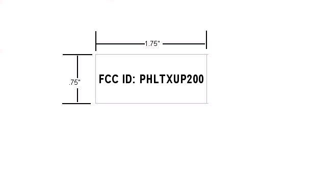
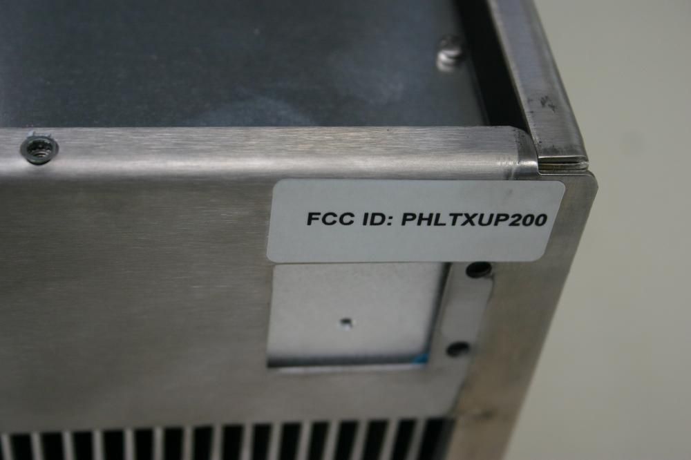
TXUP200 EXTERNAL CONSTRUCTION PHOTOS FRONT VIEW TOP VIEW CLOSE-UP REAR VIEW SHOWING FCC LABEL REAR VIEW BOTTOM VIEW LEFT SIDE VIEW RIGHT SIDE VIEW
Internal Photos
TXUP200 INTERNAL CONSTRUCTION PHOTOS FRONT VIEW FRONT INSIDE WITH FILTER REMOVED LEFT INSIDE VIEW RIGHT INSIDE VIEW REAR VIEW REAR VIEW WITHOUT FILTER
Operational Description
TXUP200 OPERATIONAL DESCRIPTION The TXUP200 consists of the VEGA exciter and the AUTV/250LD amplifier assemblies. The VEGA exciter produces a TV signal on the desired channel of operation from the video and audio supplied to the VEGA. Both video and IF signal processing occur to the signal before it is converted to the desired channel and amplified to a higher power. The amplifier AUTV/250LD is an apparatus designed to be used as final power stage or driver for higher power amplifiers in the UHF TV band. It is able to supply a power of 250W (peak sync.) in class AB and is completely realized with LDMOS technology. The power supply of the apparatus is given by a switching power supply for the RF power module and a traditional transformer for the control board. The protection board uses all the potential of a microprocessor to check all the parameters of the amplifier module and the voltage of the power supply. An output band-pass filter provides for the attenuation of the spurious products. The final result is a compact apparatus, it is all inside a standard 19”-4U cabinet, with a very good price-to-quality ratio.
Parts List/Tune Up Info
33 COMPONENT LIST SCH0192AR0 REF. DESCRIPTIONELETTRONIKA CODEPage 1/3 R12200Ω 1/4W 1206 SMD RESISTOR00045A R22200Ω 1/4W 1206 SMD RESISTOR00045A R32200Ω 1/4W 1206 SMD RESISTOR00045A R42200Ω 1/4W 1206 SMD RESISTOR00045A R51200Ω 1/4W 1206 SMD RESISTOR00042A R61200Ω 1/4W 1206 SMD RESISTOR00042A R750kΩ MULTITURNS PTH TRIMMER00800 R850kΩ MULTITURNS PTH TRIMMER00800 R91200Ω 1/4W 1206 SMD RESISTOR00042A R101200Ω 1/4W 1206 SMD RESISTOR00042A R1118kΩ 1/4W 1206 SMD RESISTOR00056B R1218kΩ 1/4W 1206 SMD RESISTOR00056B R13680KΩ 1/4W 1206 SMD RESISTOR00075A R140Ω 1/4W 1206 SMD RESISTOR00001 R1550Ω 30W 1512EBX SMD RESISTOR00416A R1650Ω 60W00432 R174.7kΩ 1/4W 1206 SMD RESISTOR00049A R184.7kΩ 1/4W 1206 SMD RESISTOR00049A R193.9Ω 1/4W 1206 SMD RESISTOR00012A R203.9Ω 1/4W 1206 SMD RESISTOR00012A R213.9Ω 1/4W 1206 SMD RESISTOR00012A R223.9Ω 1/4W 1206 SMD RESISTOR00012A R231000Ω 1W 2512 SMD RESISTOR00396 R241000Ω 1W 2512 SMD RESISTOR00396 *R25= R15 (da montare se si inverte l’ingresso) *R26= R26 (da montare se si inverte l’uscita) C1470uF 50V PTH ELECTROLYTIC CAPACITOR01807B C2470uF 50V PTH ELECTROLYTIC CAPACITOR01807B C3470uF 50V PTH ELECTROLYTIC CAPACITOR01807B C4100uF 50V PTH ELECTROLYTIC CAPACITOR01795 C5100uF 50V PTH ELECTROLYTIC CAPACITOR01795 C61nF ATC 100B CAPACITOR OR EQUIVALENT01145 C71nF ATC 100B CAPACITOR OR EQUIVALENT01145 C8 x 22 x 100nF ATC CAPACITOR OR EQUIVALENT01065H C9 x 22 x 100nF ATC CAPACITOR OR EQUIVALENT01065H C10 x 44 x 100pF ATC 100B CAPACITOR OR EQUIVALENT01135 C11 x 44 x 100pF ATC 100B CAPACITOR OR EQUIVALENT01135 C12100nF 1210 SMD CAPACITOR1065G C13100nF 1210 SMD CAPACITOR1065G C14100nF 1210 SMD CAPACITOR1065G C151uF 35V SMD TANTALIUM CAPACITOR01613A C161uF 35V SMD TANTALIUM CAPACITOR01613A C17100nF 1210 SMD CAPACITOR1065G 34 REF. DESCRIPTIONELETTRONIKA CODEPage 2/3 C18100nF 1210 SMD CAPACITOR1065G C1910uF 16V SMD TANTALIUM CAPACITOR01626A C2010uF 16V SMD TANTALIUM CAPACITOR01626A C21100nF 1210 SMD CAPACITOR1065G C22100nF 1210 SMD CAPACITOR1065G C23100nF 1210 SMD CAPACITOR1065G C24100nF 1210 SMD CAPACITOR1065G C251nF ATC 100B CAPACITOR OR EQUIVALENT01145 C261nF ATC 100B CAPACITOR OR EQUIVALENT01145 C271nF ATC 100B CAPACITOR OR EQUIVALENT01145 C281nF ATC 100B CAPACITOR OR EQUIVALENT01145 C2920pF ATC 100B CAPACITOR OR EQUIVALENT01123 C3020pF ATC 100B CAPACITOR OR EQUIVALENT01123 C3120pF ATC 100B CAPACITOR OR EQUIVALENT01123 C3220pF ATC 100B CAPACITOR OR EQUIVALENT01123 C331.3pF ATC 100B CAPACITOR OR EQUIVALENT01104 C341.3pF ATC 100B CAPACITOR OR EQUIVALENT01104 C35470pF ATC 100B CAPACITOR OR EQUIVALENT01143 C36470pF ATC 100B CAPACITOR OR EQUIVALENT01143 C37470pF ATC 100B CAPACITOR OR EQUIVALENT01143 C38470pF ATC 100B CAPACITOR OR EQUIVALENT01143 C394.7pF ATC 100B CAPACITOR OR EQUIVALENT01108 C404.7pF ATC 100B CAPACITOR OR EQUIVALENT01108 C41 x 22 x 1÷5pF JOHANSON SMD TRIMMER1485 C42 x 22 x 1÷5pF JOHANSON SMD TRIMMER1485 C433.6pF ATC 100B CAPACITOR OR EQUIVALENT01104B C443.6pF ATC 100B CAPACITOR OR EQUIVALENT01104B C456.8pF ATC 100B CAPACITOR OR EQUIVALENT01111 C466.8pF ATC 100B CAPACITOR OR EQUIVALENT01111 C476.8pF ATC 100B CAPACITOR OR EQUIVALENT01111 C486.8pF ATC 100B CAPACITOR OR EQUIVALENT01111 C4913pF ATC 100B CAPACITOR OR EQUIVALENT01119A C5013pF ATC 100B CAPACITOR OR EQUIVALENT01119A C518.2pF ATC 100B CAPACITOR OR EQUIVALENT01113 C528.2pF ATC 100B CAPACITOR OR EQUIVALENT01113 C538.2pF ATC 100B CAPACITOR OR EQUIVALENT01113 C548.2pF ATC 100B CAPACITOR OR EQUIVALENT01113 C5510pF ATC 100B CAPACITOR OR EQUIVALENT01117 C5610pF ATC 100B CAPACITOR OR EQUIVALENT01117 C574.7pF ATC 100B CAPACITOR OR EQUIVALENT01108 C584.7pF ATC 100B CAPACITOR OR EQUIVALENT01108 C590.3pF ATC 100B CAPACITOR OR EQUIVALENT01160 T1BLF861A RF LDMOS POWER TRANSISTOR04034 T2BLF861A RF LDMOS POWER TRANSISTOR04034 B1COAX 2:1 BALUN08491 35 REF. DESCRIPTIONELETTRONIKA CODEPage 3/3 B2COAX 2:1 BALUN08491 B3COAX 4:1 BALUN08492 B4COAX 4:1 BALUN08492 L14 TURNS SILV. COP. WIRE 1.2mm WOUND ON OD 5mm07684 L24 TURNS SILV. COP. WIRE 1.2mm WOUND ON OD 5mm07684 L3½ TURN COIL L4½ TURN COIL H1HYBRID COUPLER 3dB 90° ANAREN05368 H2HYBRID COUPLER 3dB 90° SAGE05369 NTC1NTC 100KΩ PTH00661 NTC2NTC 100KΩ PTH00661 IC1DG419DY04583 IC2DG419DY04583 DZ115V SMD ZENER DIODE03135 DZ215V SMD ZENER DIODE03135 DZ36.8V SMD ZENER DIODE03137 DZ46.8V SMD ZENER DIODE03137 DL1SMD LED DIODE - RED -03056 DL2SMD LED DIODE - RED -03056 PN964AR3PCB0643K Torretta 3x10 f/fV0774 Imballo velapack 200x125x5009983 40 COMPONENT LIST SCH0122BR1 Part Name/NumberDescriptionQty.Comps. Page 1/2 CC 100nF-S 01065C01065C Y5V 1206 COND23C1-2, C8, C11, C14, C21, C22, C24-32, C34, C40, C42, C44, C47, C49-50 CC 15pF-S 0108801088 SMD 1206 COND2C12-13 CC 1nF-S 0109601096 SMD 1206 COND5C15, C17-18, C20, C33 CC 1uF100V-S 01760A01760A Y5V 1206 COND8C3-7, C9, C23, C35 CC 2nF2 2kV 01045A01045A CERAMIC COND3C36-38 CE 100uF25V-S 01793B01793B ELETTR SMD COND2C41, C43 CE 10uF35V-S 01778A01778A ELETTR SMD COND4C10, C45-46, C48 CE 2200uF25V 0181301813 ELETT. COND.1C39 CE 22uF16V-S01780A ELETTR SMD COND2C16, C19 D 1N4148-S 0300203002 SMD DIODE7D1-5, D9-10 DB KBL04 0304203042 BRIDGE DIODE1PT1 DIS DMC16230 03072B03072B DISPLAY1LCD1 DL LEDG5 0306003060 GREEN LED DIODE 5mm1DL6 DL LEDR5 0306103061 RED LED DIODE 5mm1DL7 DL LEDY5 03054B03054B YELLOW LED DIODE 5mm1DL8 FUSE 1A MICRO FUSEFUS00007 + FUS00006 PORTA FUSI1F1 IC 78M05 04301B04301B SMD VOLTAGE REGULATOR1IC12 IC 78M12 4307B04307B SMD VOLTAGE REGULATOR1IC11 IC 79M08 04304A04304A SMD VOLTAGE REGULATOR1IC14 IC INA16804600A SMD INTEG CIRCUIT2IC6-7 IC LM393-S 0463904639 SMD INTEG CIRCUIT1IC5 IC LMV324M-S 04658B04658B SMD INTEG CIRCUIT2IC4, IC8 IC MAX232-S 04804B04804B SMD INTEG CIRCUIT1IC2 IC MAX3080-S 0477004770 SMD INTEG CIRCUIT1IC1 IC MC14094BD 0471804718 SMD INTEG CIRCUIT1IC9 IC PIC16F877 486904869 + 07509C INTEG CIRCUIT1IC3 IC TC7662BCOA 04758A04758A SMD INTEG CIRCUIT1IC13 IC ULN2003A 487004870 SMD INTEG CIRCUIT1IC10 IND 2u2H-S 05020A05020A INDUCTOR1L1 J CON HD515V/05-4PVE02881 + 02882 PANDUIT PCB CONN2J9-10 J FC-10P 02697-0269902697+02699…
Text truncated - open the document above for the full version.
Schematics
24 26 32 38 39 43 45 SP500-48 SWITCHING POWER SUPPLYE0013 MAIN FEATURES - Universal AC input / Full range - Built-in active PFC function, PF>0.95 - Protections: Short circuit / Over load / Over voltage / Over temp. - Forced air cooling by built-in DC fan - Built-in cooling Fan ON-OFF control - Built-in remote sense function - Fixed switching frequency at 110kHz MECHANICAL SPECIFICATION 170 150 50 93 2-M3 L=16mm max.2-M3 L=4mm max. 9.511 . 5 811 . 5 120 15141312111098 7654321 7A50/60Hz 100-240VAC INPUT (AC ) -S-V+24V 20A+S +V ADJ. SP-500-24 E 183223 LEVEL5 R.C.G.LNFGNCNCR.C. PIN N°ASSIGNMENTPIN N°ASSIGNMENT 1AC/L7R.C. 2AC/N8 +S 3FG9 ~ 11DC OUTPUT +V 4, 5NC12 ~ 14DC OUTPUT -V 6R.C.G.15 -S 48 SPECIFICATIONS Frequency470 - 860MHz ConnectorsN Insertion loss0.55dB Typ. @ V.C. Return loss26dB Operating temperature-10° to +50°C Bandwidth8MHz Selectivity @V.C.-5.5/+11-30dB Selectivity @V.C.-11/+16.5-22dB Weight1.2kg 3 SECTION BANDPASS FILTER WITH 2 NOTCH ELEMENTS - COMB-LINE STRUCTURE, INDUCTIVE COUPLING IRISES; CONSTANT BANDWIDTH, VERY EASY TO TUNE - EXACT GENERALIZED CHEBISHEV DESIGN GIVING MAXIMUM SELECTIVITY AND MINIMUM GROUP DELAY VARIATION. UHF TV OUTPUT FILTER IMD SUPPRESSOR06604A
Test Report
TEST REPORT ELETTRONIKA S. r. l. TXUP200 TV TRANSMITTER TECHNICAL REPORT INTRODUCTION The following information is provided to support the technical performance of the ELETTRONIKA S. r. l. TXUP200 TV Transmitter. The information is supplied for broadcast TV service according to applicable portions of FCC rules contained in Part 2, Part 73, and 74. 1. Power Output Measurements as indicated by FCC Rule Part 2.1046. 2. Frequency Measurements as identified by FCC Rule Part 2.1055. 3. Visual Frequency response measurements of the transmitter to be within the window specified by FCC Rule Part 74.750. 4. Occupied BW of aural signal specified by FCC Rule Part 2.1079. 5. Aural frequency response as identified by FCC Rule Part 73.687 6. Measurement of conducted harmonics and spurs +/- 3 MHz outside of channel as specified by FCC Rule Part 74.750 and Part 2 Rule 2.1051. 7. Measurement of cabinet radiation of spurs and harmonics as specified in FCC Rule 2.1053 and 2.1057. 8. Measurements of voltage and current to final amp stage as outlined in FCC Rule 2.1033. Measurements were conducted at transmitter visual power output levels of 250 watts peak of sync and 62.5 watts peak of sync and constitute the range of power for which type certification is sought. The corresponding aural power levels are 25 watts and 6.25 watts. Measurements were taken on a unit with visual carrier frequency of 567.25 MHz and an aural carrier frequency of 571.75 MHz. All test equipment was calibrated prior to the use of the equipment by the supplier of the test equipment. RF POWER OUTPUT The equipment was configured as below shown in Figure 1. The loss through the RF output cable, and attenuator was calibrated at the frequency of operation. In this case, the Bird 4391 wattmeter was inserted before the attenuator to permit power measurements to be made. The video generator was configured to produce a signal with 0 IRE video and sync. The audio generator and aural carrier were not energized. The visual portion of the transmitter was energized and the power was increased to the desired output power. The power was read on the Bird wattmeter. The TV demodulator and VM-700 were used to verify that sync compression was not causing distortion of the measurement. The aural carrier was energized and its output level was then raised to meet the precise 10 dB Visual/aural power ratio as observed on the spectrum analyzer. POWER OUTPUT Bird Power Meter reading Bird Power Meter reading at high power= 150 watts at low power= 37 watts Peak of sync power = 1.68 times Peak of sync power = 1.68 times average power reading with a black average power reading with a black picture and “0” setup picture and “0” setup Peak of sync power = 150 x 1.68 Peak of sync power = 37 x1.68 = 252 watts = 62.2 watts TEST EQUIPMENT CONFIGURATION TWO FIELDS SHOWING CORRECT MODULATION DEPTH FOR REFERENCE WHITE & SYNC LEVELS AT 250 WATTS AND AT 62.5 WATTS Power Output = 250 watts Power Output = 62.5 watts FREQUENCY STABILITY MEASUREMENTS Frequency stability is provided by the VEGA exciter. The VEGA exciter has been type certified. Since no new frequency determining components are involved with this transmitter, there is no need to re- establish the frequency stability performance. The frequency stability versus temperature and line voltage data can be examined using the records available on the FCC website. The pertinent type certification FCC ID is PHLVEGA.
Test Report
VISUAL TRANSMITTER FREQUENCY RESPONSE MEASUREMENTS The test equipment configuration of Figure 1 was used with the video generator supplying the video input waveform. For this test, the aural carrier was left energized. A variable frequency sine wave input video waveform was used. The RF sideband output level was measured for the sidebands below and above the visual carrier. The frequency response was plotted. A spectrum plot is provided for the transmitter running at 250 Watts to confirm that the radiated envelope meets the requirements as outline in Part 74 Rule 750. POWER OUTPUT = 250 WATTS
Test Report
OCCUPIED BANDWIDTH MEASUREMENTS The test equipment was configured as in Figure 1. The aural carrier was energized and increased in power until the desired Visual to Aural power ratio of 10 dB was met. The aural input signal was a 15 kHz sine wave taken from the audio generator. The aural deviation was increased until the desired level (85% of 25 kHz = 21.25 kHz) was indicated on the modulation analyzer. The output spectrum was observed on the spectrum analyzer noting the requirements as identified in FCC Rule Part 2.1079. As can be observed, the output spectrum meets these requirements. OCCUPIED BANDWIDTH—POWER OUTPUT = 250 watts Visual, 25 watts Aural (Scan width = 200 kHz) OCCUPIED BANDWIDTH—POWER OUTPUT = 62.5 Watts Visual, 6.25 Watts Aural (Scan width = 200 kHz)
Test Report
AURAL FREQUENCY RESPONSE The equipment configuration of Figure 1 was used. The visual and aural carriers were energized and the aural carrier was modulated by an audio frequency generator. A reference level was set at 200 Hz and the audio generator level was adjusted to achieve 25 kHz deviation at each modulating frequency. The following table of audio response was obtained by dividing the output audio level by the input level. This table is plotted on the graph shown on the next page below. Because the window is drawn with “zero” being on the top of the tolerance window, the reference at 200 kHz was started at -1 dB on the plot and all data points were shifted down in amplitude accordingly. By reviewing the graph on the following page, the audio response is determined to meet the requirements. TABLE OF AMPLITUDE VERSUS FREQUENCY RESPONSE DATA Frequency Decibels [Hz] [dB] 100Hz -0.1 200Hz 0 500Hz 0.2 1kHz 1.0 2kHz 2.9 5kHz 8.3 10kHz 13.6 13kHz 15.5 15kHz 16.6 AURAL FREQUENCY RESPONSE GRAPH WITH LIMITS
Test Report
CONDUCTED SPURIOUS AND HARMONICS The following photographs indicate the spurious performance (> +/- 3 MHz) from the designated TV channel. As can be seen from the photos (one taken at 250 Watts and the other taken at 62.5 Watts), the spurious levels are below 60 dB relative to the peak of sync of the visual carrier. The top center of the screen indicates the true peak of sync value when the vertical interval portion of the picture is present. These photos indicate the desired 10 dB visual to aural power ratio as the scale per division is 10 dB. POWER OUTPUT = 250 Watts POWER OUTPUT = 62.5 Watts CONDUCTED HARMONIC OUTPUTS The following data indicates the harmonic performance of the TXUP200. Photographs of the spectrum evaluating all harmonics are shown below. The second harmonic is visible in the photos below. The pictures indicate that the harmonic levels are well below 60 dB compared to the top of the screen which represents visual sync peak power. POWER OUTPUT = 250 Watts POWER OUTPUT = 62.5 Watts Both photographs indicate the fundamental frequency at 567 MHz. The fundamental frequency visual peak of sync reference value is located at the top of the screen on these photographs. The values indicate that the required performance of -60 dB is met.
Test Report
CABINET RADIATION The transmitter and test equipment were configured as shown below including the angles of measurement with respect to the transmitter cabinet. The transmitter was operated at 250 watts peak sync power with a 10 dB visual/aural ratio with the video input signal being a Color Bars signal. In this case the fundamental frequency was set to 801 MHz because there was interference on 567 MHz. The free space path loss and antenna gain characteristics were obtained at the fundamental frequency and at each of the harmonics of the visual carrier frequency in order to accurately assess the level of the signal radiated from the cabinet. Radiation from the cabinet was measured with 4 different physical rotation angles: 0, 90, 180, and 270 degrees (0 degrees being the front of the cabinet). All spectral components above -80 dB referenced to peak sync power radiated from the cabinet were recorded. The values are tabulated in the table on the next page following the photos. TEST EQUIPMENT CONFIGURATION Spectrum Analyzer TXUP200 XMTR Dummy Load Receiving Antenna TXUP200 0° Front 90° 180° 270° As indicated in the spreadsheet data, the worst case calculation was 64.7 dB at the tenth harmonic. Where measured values were above the noise floor, the worst case level was 74.7 dB. The photograph shown below indicates the physical test configuration and the test condition where the 74.7 dB measurement was recorded. The main limitation is the noise floor of the spectrum analyzer. The measurement tables for the all views of the transmitter at each frequency are shown following the picture. The results indicate that all radiated harmonics meet the FCC requirement of 60 dB as outlined in FCC rule 2.1053 and 2.1057. CABINET RADIATION DATA TXUP200 250 W CABINET RADIATION SPREADSHEET 250 W Front View 250 W = 54 dBm Corrected level must be less than -6 dBm Distance is 30 feet Harmonic Frequency Measured Cable Antenna Path Corrected Required Comparison to transmit level MHz Level Loss Gain Loss Level Level dB Xmit freq. 735.25 -42 0.8 7.3490.5 -6 dBm N/A 2nd 1470.5 -74 1.2 6.955-24.7 -6 dBm -78.7 3rd 2205.75 -86 1.5 6.558.6-32.4 -6 dBm -86.4 4th 2941 -86 2.1 6.261.1-29 -6 dBm -83 5th 3676.25 -86 2.3 6.863-27.5 -6 dBm -81.5 6th 4411.5 -86 2.6 7.364.6-26.1 -6 dBm -80.1 7th 5146.75 -86 3.2 7.665.9-24.5 -6 dBm -78.5 8th 5882 -86 3.7 667.1-21.2 -6 dBm -75.2 9th 6617.25 -80 4.2 5.668.1-13.3 -6 dBm -67.3 Noise Floor changes 10th 7352.5 -80 4.9 4.669-10.7 -6 dBm -64.7 Noise Floor changes NOTES: Antenna AH SYSTEMS SAS-510-7 S/N 118 CAL 1-11-06 Spectrum Analyzer HP 8593E S/N No # Cable RG213, 12 foot length Load BIRD 8932-115 S/N 1399 Video Source Tektronix 1910 S/N B010833 (color bars) Aural Carrier =-10 dB Spectrum analyzer RBW 100 kHz VBW 10kHz Exciter is VEGA Note: The spectrum analyzer noise floor increased 6 dB for data at the 9 th and 10 th harmonics. This is why these measured values are higher than the measured values at the previous harmonics. CABINET RADIATION SPREADSHEET 250 W Left side View 250 W = 54 dBm Corrected level must be less than -6 dBm Distance is 30 feet Harmonic Frequency Measured Cable Antenna Path Corrected Required Comparison to transmit level MHz Level Loss Gain Loss Level Level dB Xmit freq. 735.25 -44 0.8 7.349-1.5 -6 dBm N/A 2nd 1470.5 -70 1.2 6.955-20.7 -6 dBm -74.7 3rd 2205.75 -86 1.5 6.558.6-32.4 -6 dBm -86.4 4th 2941 -86 2.1 6.261.1-29 -6 dBm -83 5th 3676.25 -86 2.3 6.863-27.5 -6 dBm -81.5 6th 4411.5 -86 2.6 7.364.6-26.1 -6 dBm -80.1 7th 5146.75 -86 3.2 7.665.9-24.5 -6 dBm -78.5 8th 5882 -86 3.7 667.1-21.2 -6 dBm -75.2 9th 6617.25 -80 4.2 5.668.1-13.3 -6 dBm -67.3 Noise Floor changes 10th 7352.5 -80 4.9 4.669-10.7 -6 dBm -64.7 Noise Floor changes Note: The spectrum analyzer noise floor increased 6 dB for data at the 9 th and 10 th harmonics. This is why these measured values are higher than the measured values at the previous harmonics. CABINET RADIATION SPREADSHEET 250 W Right side View 250 W = 54 dBm Corrected level must be less than -6 dBm Distance is 30 feet Harmonic Frequency Measured Cable Antenna Path Corrected Required Comparison to transmit level MHz Level Loss Gain Loss Level Level dB Xmit freq. 735.25 -51 0.8 7.349-8.5 -6 dBm N/A 2nd 1470.5 -72 1.2 6.955-22.7 -6 dBm -76.7 3rd 2205.75 -86 1.5 6.558.6-32.4 -6 dBm -86.4 4th 2941 -86 2.1 6.261.1-29 -6 dBm -83 5th 3676.25 -86 2.3 6.863-27.5 -6 dBm -81.5 6th 4411.5 -86 2.6 7.364.6-26.1 -6 dBm -80.1 7th 5146.75 -86 3.2 7.665.9-24.5 -6 dBm -78.5 8th 5882 -86 3.7 667.1-21.2 -6 dBm -75.2 9th 6617.25 -80 4.2 5.668.1-13.3 -6 dBm -67.3 Noise Floor changes 10th 7352.5 -80 4.9 4.669-10.7 -6 dBm -64.7 Noise Floor changes Note: The spectrum analyzer noise floor increased 6 dB for data at the 9 th and 10 th harmonics. This is why these measured values are higher than the measured values at the previous harmonics. CABINET RADIATION SPREADSHEET 250 W Back side View 250 W = 54 dBm Corrected level must be less than -6 dBm Distance is 30 feet Harmonic Frequency Measured Cable Antenna Path Corrected Required Comparison to transmit level MHz Level Loss Gain Loss Level Level dB Xmit freq. 735.25 -41 0.8 7.3491.5 -6 dBm N/A 2nd 1470.5 -74 1.2 6.955-24.7 -6 dBm -78.7 3rd 2205.75 -86 1.5 6.558.6-32.4 -6 dBm -86.4 4th 2941 -86 2.1 6.261.1-29 -6 dBm -83 5th 3676.25 -86 2.3 6.863-27.5 -6 dBm -81.5 6th 4411.5 -86 2.6 7.364.6-26.1 -6 dBm -80.1 7th 5146.75 -86 3.2 7.665.9-24.5 -6 dBm -78.5 8th 5882 -86 3.7 667.1-21.2 -6 dBm -75.2 9th 6617.25 -80 4.2 5.668.1-13.3 -6 dBm -67.3 Noise Floor changes 10th 7352.5 -80 4.9 4.669-10.7 -6 dBm -64.7 Noise Floor changes Note: The spectrum analyzer noise floor increased 6 dB for data at the 9 th and 10 th harmonics. This is why these measured values are higher than the measured values at the previous harmonics. VOLTAGES AND CURRENTS TO FINAL AMPLIFIERS Final amplifier DC voltage and current measurements were made with the transmitter operating at 250 Watts power output and at 62.5 watts power output. A video input si…
Text truncated - open the document above for the full version.
Test Report
FREQUENCY STABILITY MEASUREMENTS Frequency stability versus temperature and line voltage was measured in a controlled environment. For these tests the exciter RF output was fed to a frequency counter that has better than a 1ppm accuracy. The test equipment configuration is shown below. Frequency Stability versus line voltage variation Frequency Stability versus temperature The Variac was adjusted for nominal voltage and the frequency was recorded. Then the variac was adjusted to 85% and 115% of the nominal voltage and the frequency was recorded at each voltage level. The results are tabulated below. LINE VOLTAGE (Volts) Visual Frequency (MHz) Aural Frequency (MHz) 93.5 (85%) 597.249983 601.749983 110 (nominal) 597.250046 601.750046 126.5 (115%) 597.249978 601.749978 For the temperature stability measurements the exciter was placed inside a temperature chamber equipped with temperature controller. The exciter frequency was measured on the frequency counter. Measurements were first recorded at room temperature. The temperature in the chamber was changed to each of the points identified in the table below. The chamber followed a prescribed rate of change to reach each temperature and was then allowed to stabilize at the desired temperature at which time frequency measurements were made. Temperature °C Visual Frequency (MHz) Aural Frequency (MHz) 50 597.249976 601.749976 45 597.250003 601.750003 35 597.250031 601.750031 25 597.250046 601.750046 15 597.250047 601.750047 +5 597.250048 601.750048 -5 597.250051 601.750051 -15 597.250057 601.750057 -25 597.250060 601.750060 -30 597.250066 601.750066 The recorded data indicates that the total shift in frequency was 90 Hz and thus frequency stability requirements of FCC Rule 2.1055 were met. Exciter Frequency Counter Variac AC Input AC OutputRF Output Exciter Frequency Counter Temperature Chamber RF Output
Contact Information
Applicant
Francesco Paparella(Design Omologation and Compliance Mgr)
Technical Contact
Greg Best Consulting Inc.Gregory Best
[email protected]816-792-2913
9223 N. Manning Avenue · Kansas City, Missouri · United States
Technical Specifications
| # | Rule Parts | Frequency Range | Power Output | Emission | Tolerance |
|---|---|---|---|---|---|
| 4 | 73,74 | 614 MHz - 806 MHz | 25 W | 250KF3E | 1000 Hz |
Other Applications from Elettronika S.r.l.
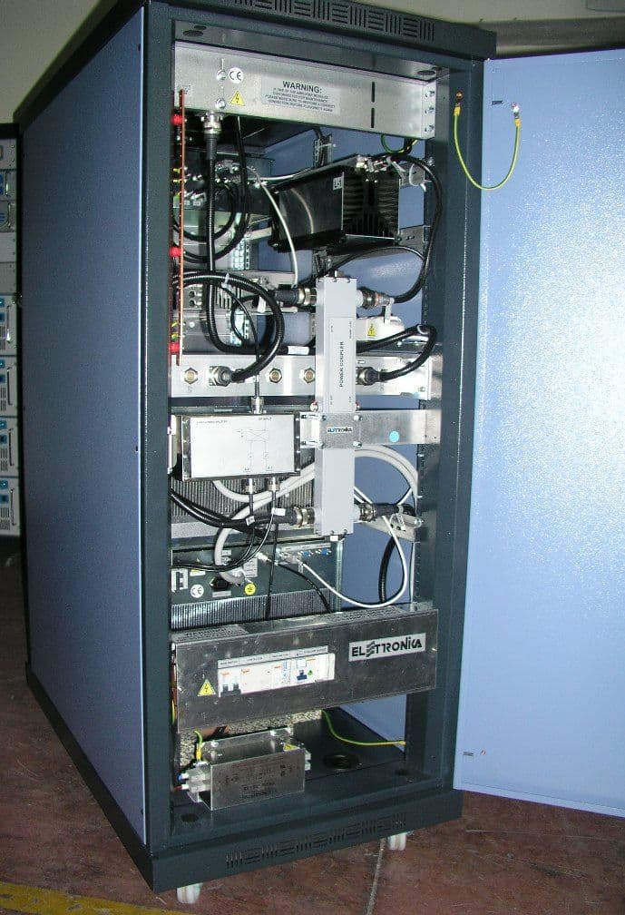
PHLTXUD1000A
Jul 07, 20101000 W ATSC Transmitter
Equipment Class
TBC - Licensed Broadcast Station Transmitter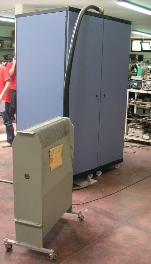
PHLTXUD3000A
Jun 17, 20103000 Watt ATSC Transmitter
Equipment Class
TBC - Licensed Broadcast Station Transmitter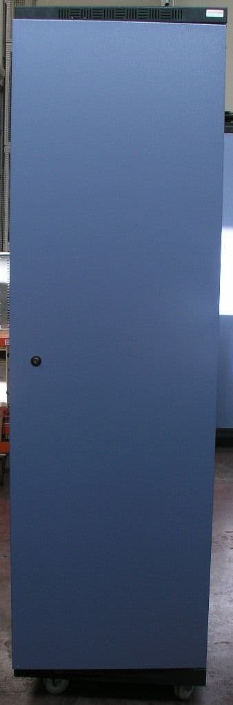
PHLTXUD2000A
Jun 09, 20102000 Watt ATSC Transmitter
Equipment Class
TBC - Licensed Broadcast Station Transmitter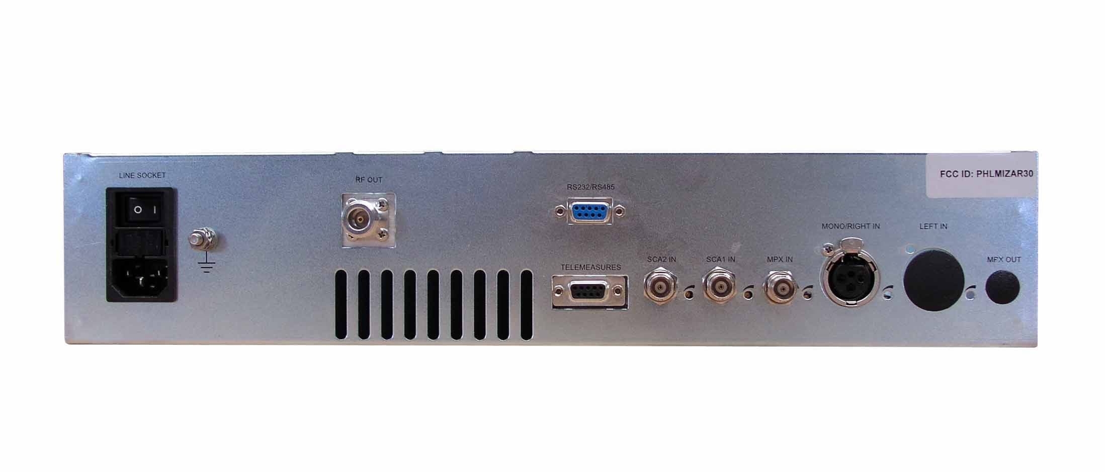
PHLMIZAR30
Jul 01, 200830 Watt FM Broadcast Transmitter
Equipment Class
TBC - Licensed Broadcast Station Transmitter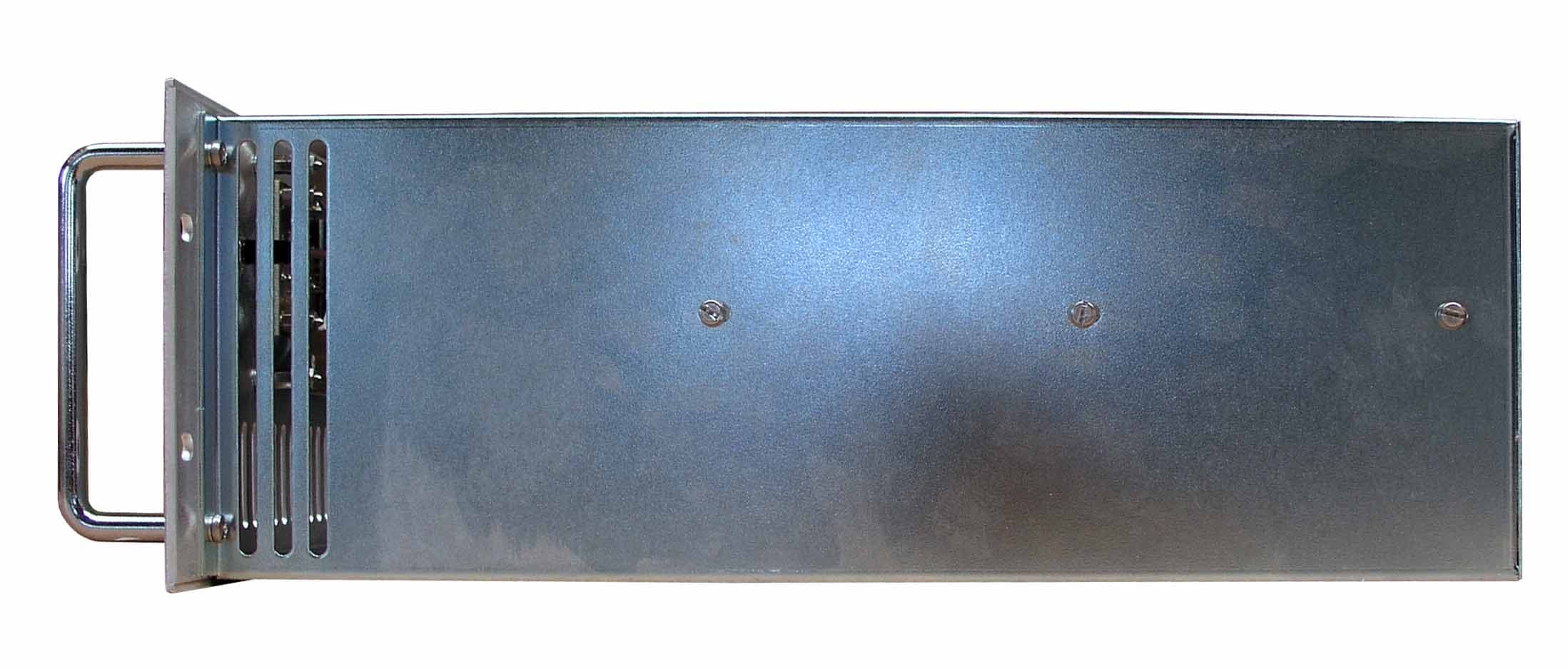
PHLMIZAR300
Jul 01, 2008300 Watt FM Broadcast Transmitter
Equipment Class
TBC - Licensed Broadcast Station Transmitter