PHLTXUP1000010 kW Analog TV Broadcast Transmitter
Elettronika S.r.l.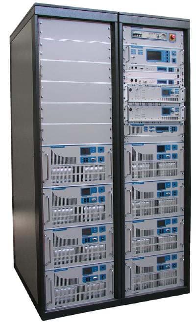
Click to zoom
Application Details
- Equipment Class
- TBC - Licensed Broadcast Station Transmitter
- Date of Grant
- Jan 30, 2007
- Application Purpose
- Original Equipment
- Date of Application
- Dec 03, 2006
- Equipment Note
- 10 kW Analog TV Broadcast Transmitter
- Frequency Range
- 614.00000000 - 806.00000000
- Company
- Elettronika S.r.l.
- Country
- Italy
Documents & Files

Document Text
Text extracted from the exhibit documents filed with the FCC. Open a document above to read the original.
Users Manual
TXUP10000LD LDMOS - UHF TV Solid State Transmitter General description CODE: STT028A TITLE: TXUP10000LD REV: 0 DATE: 08/07/05 SS 96 Km 113 70027 Palo del Colle (Ba) ITALY Tel. +39 (0)80 626755 Fax +39 (0)80 629262 E-mail: [email protected] Web site: http://www.elettronika.it Registration number: IT-17686 Registration number: IT-24436 DESCRIPTION The TXUP10000LD belongs to the High Power UHF products family of Television Transmitters fully in solid state technology. The TXUP10000LD series represents the 10kW TV Transmitters operating in the IV/V Band for Common amplification process (separate amplification available) of the Vision and Sound carriers. This Transmitters family has been designed to offer to the customer high performances, high reliability and greater simplicity in their operation and maintenance procedures. The Vision and Sound signal processing is provided for all TV Standards and all types of Audio applications (Mono & Dual sound - NICAM) together with colour systems such as PAL - NTSC - SECAM. Thanks to the amplitude and phase pre-correction circuit, it is possible to cancel the distortions in the output stage, thus cutting down the operating costs. The RF transposition in the driver is carried out by a synthesizer with various possibilities of accuracy and stability as well as precision offset locked by internal or external frequency reference. The RF amplifier is made up by eight RF modules installed in a power rack, the modules are dedicated for the Vision and Sound carriers common amplification. The amplifiers employ solid state LDMOS technology in order to obtain wide band, reliability, and high efficiency. Each RF module has a built-in switching-mode power supply unit, self-protected against overcurrents and overvoltages, as well as overtemperature and VSWR for RF parameters. The cooling system is fully contained into the transmitter. The control unit provides full management of the transmitter without the presence of the operator, the system includes a central controller and several peripheral units installed in each RF module and rack. The control device includes a fault finding system to detect equipment malfunctions and locate the faulty subassembly which needs to be replaced. The interlock circuit is independent on the software and remains always operational whether computer control is present or not. The operator interface is made by a high resolution LCD graphic display and a simple keyboard, the menu is very friendly and easy to use. The Control Unit can be fully controlled in REMOTE mode via link or via modem in RS232 or other interface. The equipment design allows the soft degradation (RF power loss) for several transistors faults. - TECHNICAL SPECIFICATIONS RF SECTION Frequenchy range ............................................................................................................................................470 - 860MHz Output power ........................................................................................................................................................10kW PEP Audio / Video power ratio ....................................................................................... 10/1 single sound - 20/1/0.2 dual sound Out stage technology .............................................................................................................................Solid State LDMOS Audio / Video amplification......................................................................................................................................Common Standards................................................................................................................................................................ G, K, I, M Audio transmission ...................................................................... FM single sound - Dual sound coding IRT - NICAM 728 Harmonics and suppression emission ..................................................................................... In compliance with CCIR rec. Intermodulation products from audio and video ..................................................................................................... < = 56dB Frequency stability .........................................................................................................................2,5ppm (option 0,05ppm) VIDEO SECTION Video input.............................................................................................................................................BNC 75Ω connector Nominal input level..............................................................................................................................................1Vpp ±6dB Return loss ............................................................................................................................................................... > = 30dB DC Restoration........................................................................... Clamped to the blanking level without affecting the burst White limiter................................................................................. At 90% picture signal without affecting the chrominance Transmission characteristics Sideband spewctrum response ....................................................................................................According to the standard Amplitude frequency response .................................................................................................... According to the standard Group delay variation without receiver pre-correction and TV demodulator flat ................................................... < = ±35ns Non linearity distortion (10 to 75% mod.) ................................................................................................................... < = 5% Differential gain (10 to 75% mod.).......................................................................................................…
Text truncated - open the document above for the full version.
Users Manual
1 LDMOS TV SOLID STATE AMPLIFIER AUTV/1500LD User’s manual 2 This page is intentionally blank 3 Section 1 - Information Contents: 1.1 Description 1.2 Technical characteristics 4 1.1 DESCRIPTION The AUTV/1500LD is an amplifier operating into Band IV-V for common amplification process of the Vision and Sound carriers. The amplifier has been designed to offer to the customer high performances, high reliability and greater simplicity in his operation and maintenance procedures. The amplifiers modules employ all solid state LDMOS technology in order to obtain high gain, wide- band performances, very good linearity, reliability and high efficiency. The equipment design allows the soft degradation (RF power loss) for several transistor faulty: in fact the output combiner uses RF power resistors for unbalancing power dissipation. The unit is enclosed in a cabinet for 19”- 6U rackmounting. AUTV/1500LD TV AMPLIFIER 5 1.2 TECHNICAL CHARACTERISTICS RF SECTION Frequency range470 - 860MHz Output power1300W PEP Video/Sound power ratio10/1 Out stage technologySolid State LDMOS Vision-Sound amplificationCommon I.M.D. (-8, -10, -16dB)Better than -54dB StandardsG, K, N Spurious and harmonics levelIn compliance with CCIR rec. RF Output impedance50Ω RF Output connector7/16” GENERAL Power supply230Vac, ±10%, 50/60Hz 400Vac 3P+N (on request) Power consumption3400VA at black level RS232 SocketDB9 Connector (on front panel) RS485 SocketDB9 Connector (on rear panel) Telemeasuring socketDB9 Connector (on rear panel) AGC SocketDB9 Connector (on rear panel) Power factor> = 0.9 Ambient temperature-5° to +45°C Relative humidity20% - 90% AltitudeUp to 2.500 meters CoolingForced air CabinetRack 19”-6U Weight70kg PROTECTION THR. FWD Power1500W REF Power150W Unbalacing300W Temperature75°C I DC 18A V DC Min 10V - Max 33,5V 6 This page is intentionally blank 7 Section 2 - Installation Contents: 2.1 Operating environment 2.2 Preliminary operations 2.3 Telemeasuring socket connections 2.4 RS232, RS485 and AGC socket connections 2.5 Preventive maintenance Front panel Rear panel 8 2.1 OPERATING ENVIRONMENT You can install the apparatus in a standard component rack or on a suitable surface such as a bench or desk. In any case, the area should be as clean and well-ventilated as possible. Always allow for at least 2 cm of clearance under the unit for ventilation. If you set the apparatus on a flat surface, install spacers on the bottom cover plate. If you install the apparatus in a rack, provide adequate clearance above and below. Do not locate the apparatus directly above a hot piece of equipment. 2.2 PRELIMINARY OPERATIONS Correct installation of the equipment is important for maximum performance and reliability. Antenna and earth connections must be installed with the greatest care. The equipment adjustment isn’t need, because the unit is completely adjusted by our technical staff. This is the installation procedure: 1. connect the power supply cable of the exciter to the auxiliary socket on the rear panel of the amplifier; 2. connect the power supply cable of the amplifier to the electric network (230VAC). If there is the Isolator Transformer, the amplifier is provided with cable and plug; 3. connect the exciter / antenna cables respectively to the RF IN and RF OUT on the rear panel of the amplifier. WARNING!!! FOR ELECTRICAL SAFETY REASONS AND IN ORDER TO KEEP THE APPARATUS SAFE, THE GROUND TERMINAL OF THE APPARATUS MUST BE CONNECTED TO THE EXISTING GROUND- ING SYSTEM AND NOT BY USING THE SHIELD OF THE OUTPUT COAXIAL CABLE. 2 3 1 Three-Phase cabling Monophase cabling 9 When the apparatus is put within a combined system it is directly connected to the input splitting and output combining systems. Before fully powering the apparatus, check that the output connections of the coaxial cable to the antenna system are working. In order to this it is possible to check the indication of the reflected power at low power levels. Only if the SWR indication on the display is 0, the output power can be slowly increased. At maximum output power, some watts might be shown as reflected power. 2.3 TELEMEASURING SOCKET CONNECTIONS DB9 Socket 2.4 RS232, RS485 AND AGC SOCKET CONNECTIONS PIN N°SIGNAL TYPEIN / OUTFUNCTION 1Analog OutputFWD Power 2AnalogOutputREF Power 3DigitalOutputTemperature 4DigitalInputInterlock 5GND-- 6 - 7DigitalOutputFree contact (closed when alarm) 8DigitalInput 0V = ON 5V = Normal 9DigitalInput 0V = OFF 5V = Normal PIN 123456789 FUNCTIONS -TxDRxD-GND- - - - RS232 - DB9 Socket PIN 123456789 FUNCTIONS -Rx-Rx+5VGND-Tx-Tx+- RS485 - DB9 Socket 10 AGC - DB9 Socket PIN N°SIGNAL TYPEIN / OUTFUNCTION 1GND-- 2DigitalOutput 0V = Normal 5V = AGC Alarm 3DigitalOutput 0V = Normal 5V = AGC Alarm 8AnalogOutputFWD Power 9AnalogOutputFWD Power 2.5 PREVENTIVE MAINTENANCE To ensure maximum performance and minimum repair trouble, we strongly recommend you to follow the below stated headlines for preventive maintenance: 1. check antenna installation and ground connection at regular intervals; 2. keep your apparatus clean and dry externally: this will ensure continuous functioning of the front panel controls; 3. if the apparatus has not been used for a long period of time combined with exposure to extreme environ- mental conditions, open the unit and make a visual inspection. Remove salt, water or ice with a moist cloth before turning the apparatus on. Check that the cooling fans are running freely. 4. for general maintenance and top performance, call an authorized service technician to give the apparatus and the complete antenna/earth connection installation a general check every 12-18 months; 5. check at regular intervals that the air intake located on the front panel is free of dust. If there is visible dust, remove it by means of a soft brush. 11 Front panel 1 2 3 45 6 DESCRIPTION 1LCD Display 2Function keys 3Status LEDs 4RF Monitor connector 5Main switch 6RS232 Socket 12 Rear panel 1 3 2 4 5 6 9 8 7 DESCRIPTION 1Breaker 2Power supply socket…
Text truncated - open the document above for the full version.
Cover Letter(s)
January 26, 2007 Federal Communications Commission Office of Engineering Technology 445 12 th Street SW Washington, DC 20554 Dear Sir, This letter will serve to address FCC correspondence letter 32368 regarding the type certification for the Elettronika TXUP10000 broadcast transmitter. The associated FCC ID number is PHLTXUP10000. Specifically, the correspondence letter identified above seeks additional information on how the transmitter is configured regarding whether integral components are the same for both frequency ranges of the proposed grant frequencies. As the technical consultant for Elettronika, they have authorized me to provide information which should help resolve this question. It is my technical opinion that only one set of test data needs to be submitted for both frequency ranges 470-608 MHz and 614-806 MHz based upon the design of the unit. The design of the unit is such that the transmitter works over the entire 470-806 MHz with no change of parts. The only frequency dependent parts within the transmitter are the channel filter in the exciter and transmitter final bandpass filter. The exciter filter is a passive device and consists of one item that is tuned per operating channel. Likewise the transmitter final bandpass filter is a passive device and is the same block of material but it is tuned to the desired operating channel. The performance obtained at any test frequency within the entire range of 470-806 MHz will be representative of each transmitter shipped. If there are any clarifications needed or you have any questions please give me a call at the number above. Sincerely, Greg Best President Cc Maria Quintero, Elettronika America Greg Best Consulting, Inc. 9223 N. Manning Ave. Kansas City, MO 64157 816-792-2913
External Photos
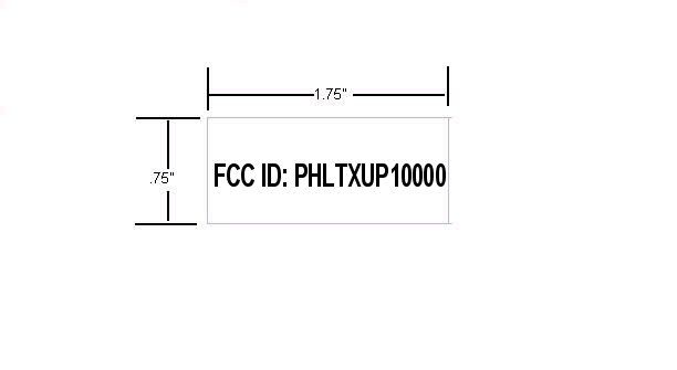
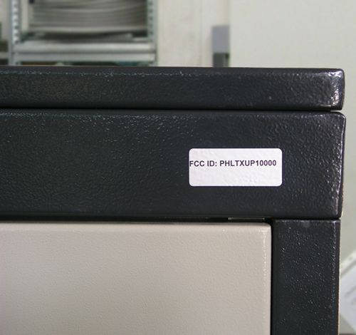
TXUP10000 EXTERNAL CONSTRUCTION PHOTOS FRONT VIEW CLOSE-UP REAR VIEW SHOWING FCC LABEL REAR VIEW
Internal Photos
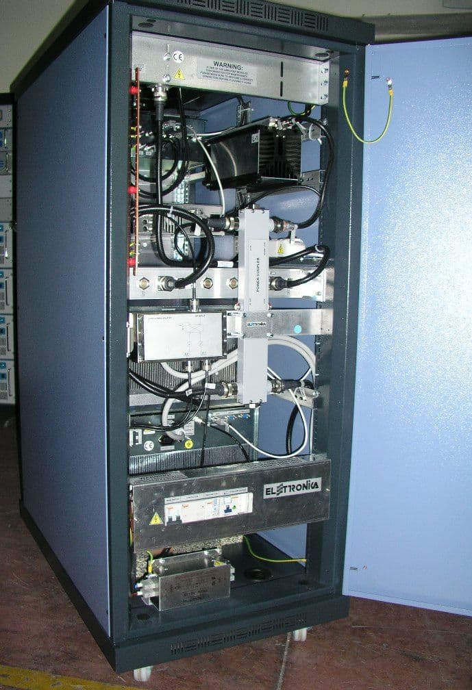
TXUP10000 INTERNAL CONSTRUCTION PHOTOS REAR VIEW TOP REAR MIDDLE REAR VIEW—DOOR OPEN BOTTOM REAR VIEW—DOOR OPEN LEFT SIDE WITHOUT SIDE PANELS RIGHT SIDE WITHOUT SIDE PANELS
Operational Description
OPERATIONAL DESCRIPTION The TXUP10000LD belongs to the High Power UHF products family of Television Transmitters fully in solid state technology. The TXUP10000LD series represents the 10kW TV Transmitters operating in the IV/V Band for Common amplification process (separate amplification available) of the Vision and Sound carriers. This Transmitters family has been designed to offer to the customer high performances, high reliability and greater simplicity in their operation and maintenance procedures. The Vision and Sound signal processing is provided for all TV Standards and all types of Audio applications (Mono & Dual sound - NICAM) together with colour systems such as PAL - NTSC - SECAM. Thanks to the amplitude and phase pre-correction circuit, it is possible to cancel the distortions in the output stage, thus cutting down the operating costs. The RF transposition in the driver is carried out by a synthesizer with various possibilities of accuracy and stability as well as precision offset locked by internal or external frequency reference. The RF amplifier is made up by eight RF modules installed in a power rack, the modules are dedicated for the Vision and Sound carriers common amplification. The amplifiers employ solid state LDMOS technology in order to obtain wide band, reliability, and high efficiency. Each RF module has a built-in switching-mode power supply unit, self- protected against overcurrents and overvoltages, as well as overtemperature and VSWR for RF parameters. The cooling system is fully contained into the transmitter. The control unit provides full management of the transmitter without the presence of the operator, the system includes a central controller and several peripheral units installed in each RF module and rack. The control device includes a fault finding system to detect equipment malfunctions and locate the faulty subassembly which needs to be replaced. The interlock circuit is independent on the software and remains always operational whether computer control is present or not. The operator interface is made by a high resolution LCD graphic display and a simple keyboard, the menu is very friendly and easy to use. The Control Unit can be fully controlled in REMOTE mode via link or via modem in RS232 or other interface. The equipment design allows the soft degradation (RF power loss) for several transistors faults.
Parts List/Tune Up Info
17 SCH0239AR0 COMPONENT LIST Part Name/NumberDescriptionQty.Comps. Page 1/2 BATT BH001RB 3093_9003093 03090 BATTERY HOLDER1BATT1 BZ AI-155 0370503705 5VDC BUZZER1BZ1 CC 100nF-S 01065C01065C Y5V 1206 COND33C10, C15, C17-19, C22, C25, C28, C38, C45, C49-52, C55, C62-63, C68-69, C78, C80-85, C87-88, C90, C92-95 CC 15pF-S 0108801088 SMD 1206 COND2C74-75 CC 1nF-S 0109601096 SMD 1206 COND20C12-14, C31-33, C42-43, C53-54, C56-58, C60-61, C66, C76-77, C79, C86 CC 1uF100V-S 01760A01760A Y5V 1206 COND <<50 V>>8C21, C23, C37, C64-65, C67, C71-72 CC 220pF-S 0109301093 SMD 1206 COND8C2-9 CC 47pF-S 0110001100 SMD 1206 COND8C20, C30, C35-36, C40-41, C48, C59 CE 10uF16V-S01626B TANT. ELETTR SMD CO8C24, C26-27, C29, C34, C39, C46-47 CE 1uF50V-S 01763A01763A ELETTR SMD COND2C89, C91 CE 220uF50V LOW ESR1799A ELETTR SMD COND LOW ESR 4C16, C44, C70, C73 CE 47uF35V-S 01790A01790A ELETTR SMD COND1C11 CE 47uF50V-S 01791C01791C ELETTR SMD COND1C1 D 1N4148-S 0300203002 SMD DIODE4D12-13, D17, D19 D 50WQ06FN03019A SMD DIODE SCHOTTKY 5,5A 1D9 D BAS85-S03024 SMD DIODE SCHOTTKY8D1-8 D BAT54S03199 SMD SCHOTTKY DIODE A-K T 6D10-11, D14-16, D18 DIS WG240128B03083 240/128 DOT MATRIX LCD1LCD1 DL KA-3528SGC 0305703057 GREEN SMD LED DIODE1DL1 DL LEDG3 0305303053 GREEN LED DIODE 3mm1DL3 DL LEDR3 0305803058 RED LED DIODE 3mm4DL2, DL4, DL6-7 DL LEDY3 0305103051 YELLOW LED DIODE 3mm1DL5 IC 24LC64 0481504815 SMD INTEG CIRCUIT1IC7 IC 74HC00-S 4762A4762A SMD INTEG CIRCUIT1IC19 IC 82B715-S 04734A04734A SMD INTEG CIRCUIT1IC17 IC CD4053BC-S 04710A04710A SMD INTEG CIRCUIT1IC12 IC LM2596S-5.004580 SMD INTEG CIRCUIT1IC14 IC LM75-S 0066800668 SMD INTEG CIRCUIT1IC8 IC LMC6482-S04632 SMD INTEG CIRCUIT1IC20 IC LMC6484-S04634 SMD INTEG CIRCUIT4IC2-5 IC M41T56 0461104611 SMD INTEG CIRCUIT1IC6 IC MAX232-S 04804B04804B SMD INTEG CIRCUIT1IC16 IC MAX3080-S 0477004770 SMD INTEG CIRCUIT1IC22 IC MAX3080-S N.M.NOT MOUTED SMD INTEG CIRCUIT 1IC18 IC MAX942CSA-S04572 SMD INTEG CIRCUIT4IC9-11, IC13 IC MB90F543PF04596 SMD INTEG CIRCUIT1IC15 IC MPC100T-450I-TT04577 SMD INTEG CIRCUIT1IC21 IC ULN2003A 487004870 SMD INTEG CIRCUIT2IC1, IC23 IND MS85 10uH-S04948 INDUCTOR 2,7A1L1 IND T100uH-1.8A 495804958 TOROIDAL-STORAGE CHOKES 1L2 18 Part Name/NumberDescriptionQty.Comps. Page 2/2 INV IN-D43A-5V03085 DC/AC MODULE1INV1 J DB9_F-0° LT02794 PCB CONNECTOR DB9 LONG T 1J6 J FC-10P 02697-0269902697+02699 PCB CONNECTOR POL2J11, J13 J FC-16P 02701-0270002701+02700 PCB CONNECTOR POL2J12, J14 J FC-26P 02855-0285402855+02854 PCB CONNECTOR POL1J10 J PAN2 0273902739 PCB CONNECTOR1J4 J PAN2 02739-40-4102739+02740+02741 PCB CONNECTO1J5 J PAN3 0270702707 PCB CONNECTOR3J1-3 J PAN3 NOT MOUNTEDNOT MOUNTED PCB CONNECTOR2J8-9 J SCREWCONN2 0285302853 PCB SCREW CONNECTOR1J7 JU JUMP3 02707-0274202707+02742 MASCHIO PAN34JP1-4 R 100R-S 00029A00029A RES 1/4W 5% SMD 12066R109, R114, R119-121, R123 R 10K-S 00053A00053A RES 1/4W 5% SMD 120637R22-27, R30, R32-33, R40, R47, R50, R57, R68, R81-82, R85, R90-101, R105-108, R116, R118, R122, R124 R 120R-S 00030A00030A RES 1/4W 5% SMD 12062R112-113 R 1K0-S 00041A00041A RES 1/4W 5% SMD 12065R46, R54, R87-88, R104 R 1K5-S 00043A00043A RES 1/4W 5% SMD 12062R110-111 R 22K-S 00057A00057A RES 1/4W 5% SMD 120611R18, R20-21, R28, R34, R36, R38-39, R41, R43-44 R 2K2-S 00045A00045A RES 1/4W 5% SMD 12068R19, R35, R37, R42, R45, R53, R59-60 R 330R-S 00035B00035B RES 1/4W 5% SMD 12062R89, R103 R 33R-S 00023A00023A RES 1/4W 5% SMD 12062R86, R102 R 470K-S 00073A00073A RES 1/4W 5% SMD 12068R48-49, R51-52, R55-56, R58, R65 R 470R-S 00037A00037A RES 1/4W 5% SMD 120630R10-17, R29, R31, R61-64, R66-67, R69-80, R83-84 R 4K7-S 00049A00049A RES 1/4W 5% SMD 12061R117 R 820R-S 00040A00040A RES 1/4W 5% SMD 12061R9 RL 30.22.24 0756907569 RELE5RLY1-5 RV 10K-S-H 0071500715 VARIABLE RESISTOR1R115 RV 1M-3266X00815 VARIABLE RESISTOR8R1-8 SW SWITCH-4DIP 90°07531A PCB DIP SWITCH 90°1SW1 SW SWITCH-8DIP07530A PCB DIP SWITCH SMD1SW2 T 06086 N 7630 76327630 7632 KTI06086 PULSANTE 24T1-4 TR BC848 0345703457 NPN SMD TRANSISTOR1TR1 XTAL 32.768k-S 0514605146 QUARTZ1XTAL1 XTAL 4MHz-S 05101A05101A QUARTZ1XTAL2 19 220VAC SWITCHING BOARDSCH0152AR0 SCH0152AR0 Component layout SCH0152AR0 COMPONENT LIST Part Name/NumberDescriptionQty.Comps. CC 2nF2 2kV 01045A01045A CERAMIC CAPACITOR3C1-3 D 1N4148 0300103001 DIODE6D1-6 FUSE OMEGA C1034FUS00008 FUSE-HOLDER 5x20 D1F1 J CON HD515V/05-6PVE02883 + 02884 PANDUIT PCB CONN1J1 J FC-10P 02697-0269902697+02699 PCB CONNECTOR POL1J9 J VASCHETTA IEC02879 VASCHETTA FEMALE PCB3J6-8 JU JUMP2 02739-0274202739+02742 MALE PAN21JP1 RL 40.31.247567C RELE3RLY1-3 20 IN/OUT DIGITAL BOARDSCH0241AR0 SCH0241AR0 Component layout SCH0241AR0 COMPONENT LIST Part Name/NumberDescriptionQty.Comps. DZ 5V1 0310903109 ZENER DIODE1DZ1 FUSE OMEGA C1034FUS00008 PORTA FUSIBILE 5x20 D1F1 J BNC-90G-PCB 203402034 PCB CONNECTOR2J2-3 J DB9-90G 0279702797 PCB CONNECTOR3J4-6 J FC-16P 02701-0270002701+02700 PCB CONNECTOR POL1J1 J SCREWCONN2 0285302853 PCB SCREW CONNECTOR1J7 J TESTP2.5mm 0791207912 TEST POINT4J8-11 R 0R0-S 0000100001 RES 1/4W 5% SMD 12067R3-9 R 10K 00530053 RES 1/4W 5%1R1 R 1K0 00410041 RES 1/4W 5%1R2 24 ANALOG INPUT BOARDSCH0110BR0 SCH0110BR0 Component layout SCH0110BR0 COMPONENT LIST Part Name/NumberDescriptionQty.Comps. CC 1206 N. M.N. M. SMD 1206 CAPACITOR17C4-20 CC 1nF-S 0109601096 SMD 1206 CAPACITOR3C1-3 J BNC-90G-PCB 203402034 PCB CONNECTOR3J1-3 J BNC-90G-PCB 2034N. M. BNC-90G5J4-8 J FC-16P 02701-0270002701+02700 PCB CONNECTOR POL1J9 R 0R0-S 0000100001 RES 1/4W 5% SMD 12066R13, R15, R17, R19, R21, R23 R 1206 N. M.N. M. RES 1/4W 5% SMD 120618R1-12, R14, R16, R18, R20, R22 R24 Z MICRO SOIC 8P N.M.SMD INTEG CIRCUIT NOT MOUNTED3IC1-3 27 Part Name CodeDescriptionQty 000010Ω 1206 SMD RESISTOR2 01041D1nF 1206 2% SMD CAPACITOR2 00221B75Ω 1206 1% SMD RESISTOR2 03207HSMS-2802*L31 DIODE2 SCH0192AR0200W UHF LDMOS AMPLIFIER MODULE9 SCH0221AR0AMPLIFIER INTERFACE1 SCH0248AR08 WAY WILKINSON1 SCH0249AR04 WAY WILKINSON Dx1 SCH0250AR04 WAY WILKINSON Sx1 SCH0251AR02 WAY WILKINSON1 SCH0252AR01500…
Text truncated - open the document above for the full version.
Schematics
14 24 25 26 42 Figure 2: Usage of the digital input signals of the telemeasures connector AGC / EXCITER The connector called J10, as the telemeasures connector and the RS485 bus, is wired to a DB9 female connector placed on the rear panel of the amplifier. This connector allow the implementation of an automatic gain control between an exciter and the amplifier. A voltage signal related to the forward output power supplied by the amplifier is provided through two pins of the AGC connector. Connecting one of these to the relevant input pin of the exciter, this can pursuit a given voltage level, so that the output power is always constant. In order to avoid that, in case of an alarm decreasing the forward power, the exciter increases its output level due to the AGC, thus damaging the amplification stages, the connector is provided with two digital output lines called AGC Alarm. Under alarm conditions, this lines are brought by the micro-controller at a low level, so that the exciter can stop the AGC. Table 4 shows the connection between the J10 connector on the board and the DB9 connector on the rear panel, along with the description of each pin (the direction of the pin is referred to the position of the micro- controller on the board). level of the interlock signal becomes high (this line has a pull-up towards the +5V power supply voltage as well) and the interlock protection activates switching off the amplifier. Note that in case the interlock protection is not used, the pin 4 of the DB9 telemeasure connector and the earth pin (pin 5) must be short circuited. Otherwise it is possible to disable the monitoring of the interlock chain from menu (see user manual). Figure 2 shows a typical usage for the digital input signals to turn on and off the amplifier and for the interlock alarm.
Test Report
TEST REPORT ELETTRONIKA S. r. l. TXUP10000 TV TRANSMITTER TECHNICAL REPORT INTRODUCTION The following information is provided to support the technical performance of the ELETTRONIKA S. r. l. TXUP10000 TV Transmitter. The information is supplied for broadcast TV service according to applicable portions of FCC rules contained in Part 2, Part 73, and 74. 1. Power Output Measurements as indicated by FCC Rule Part 2.1046. 2. Frequency Measurements as identified by FCC Rule Part 2.1055. 3. Visual Frequency response measurements of the transmitter to be within the window specified by FCC Rule Part 74.750. 4. Occupied BW of aural signal specified by FCC Rule Part 2.1079. 5. Aural frequency response as identified by FCC Rule Part 73.687 6. Measurement of conducted harmonics and spurs +/- 3 MHz outside of channel as specified by FCC Rule Part 74.750 and Part 2 Rule 2.1051. 7. Measurement of cabinet radiation of spurs and harmonics as specified in FCC Rule 2.1053 and 2.1057. 8. Measurements of voltage and current to final amp stage as outlined in FCC Rule 2.1033. Measurements were conducted at transmitter visual power output levels of 10000 watts peak of sync and 2500 watts peak of sync and constitute the range of power for which type certification is sought. The corresponding aural power levels are 1000 watts and 250 watts. Measurements were taken on a unit with visual carrier frequency of 567.25 MHz and an aural carrier frequency of 571.75 MHz. All test equipment was calibrated prior to the use of the equipment by the supplier of the test equipment. RF POWER OUTPUT The equipment was configured as below shown in Figure 1. The loss through the RF output cable, and attenuator was calibrated at the frequency of operation. In this case, the Bird 4391 wattmeter was inserted before the attenuator to permit power measurements to be made. The video generator was configured to produce a signal with 0 IRE video and sync. The audio generator and aural carrier were not energized. The visual portion of the transmitter was energized and the power was increased to the desired output power. The power was read on the Bird wattmeter. The TV demodulator and VM-700 were used to verify that sync compression was not causing distortion of the measurement. The aural carrier was energized and its output level was then raised to meet the precise 10 dB Visual/aural power ratio as observed on the spectrum analyzer. POWER OUTPUT Bird Power Meter reading Bird Power Meter reading at high power= 6000 watts at low power= 1490 watts Peak of sync power = 1.68 times Peak of sync power = 1.68 times average power reading with a black average power reading with a black picture and “0” setup picture and “0” setup Peak of sync power = 6000 x 1.68 Peak of sync power = 1490x1.68 =10080 watts = 2500 watts TEST EQUIPMENT CONFIGURATION TWO FIELDS SHOWING CORRECT MODULATION DEPTH FOR REFERENCE WHITE & SYNC LEVELS AT 10000 WATTS AND AT 2500 WATTS Power Output = 10000 watts Power Output = 2500 watts FREQUENCY STABILITY MEASUREMENTS Frequency stability is provided by the VEGA exciter. The VEGA exciter has been type certified. Since no new frequency determining components are involved with this transmitter, there is no need to re- establish the frequency stability performance. The frequency stability versus temperature and line voltage data can be examined using the records available on the FCC website. The pertinent type certification FCC ID is PHLVEGA.
Test Report
VISUAL TRANSMITTER FREQUENCY RESPONSE MEASUREMENTS The test equipment configuration of Figure 1 was used with the video generator supplying the video input waveform. For this test, the aural carrier was left energized. A variable frequency sine wave input video waveform was used. The RF sideband output level was measured for the sidebands below and above the visual carrier. The frequency response was plotted. A spectrum plot is provided for the transmitter running at 10000 Watts to confirm that the radiated envelope meets the requirements as outline in Part 74 Rule 750. POWER OUTPUT = 10000 WATTS
Test Report
OCCUPIED BANDWIDTH MEASUREMENTS The test equipment was configured as in Figure 1. The aural carrier was energized and increased in power until the desired Visual to Aural power ratio of 10 dB was met. The aural input signal was a 15 kHz sine wave taken from the audio generator. The aural deviation was increased until the desired level (85% of 25 kHz = 21.25 kHz) was indicated on the modulation analyzer. The output spectrum was observed on the spectrum analyzer noting the requirements as identified in FCC Rule Part 2.1079. As can be observed, the output spectrum meets these requirements. OCCUPIED BANDWIDTH—POWER OUTPUT = 10000 watts Visual, 1000 watts Aural (Scan width = 200 kHz) OCCUPIED BANDWIDTH—POWER OUTPUT = 2500 Watts Visual, 250 Watts Aural (Scan width = 200 kHz)
Test Report
AURAL FREQUENCY RESPONSE The equipment configuration of Figure 1 was used. The visual and aural carriers were energized and the aural carrier was modulated by an audio frequency generator. A reference level was set at 200 Hz and the audio generator level was adjusted to achieve 25 kHz deviation at each modulating frequency. The following table of audio response was obtained by dividing the output audio level by the input level. This table is plotted on the graph shown on the next page below. Because the window is drawn with “zero” being on the top of the tolerance window, the reference at 200 kHz was started at -1 dB on the plot and all data points were shifted down in amplitude accordingly. By reviewing the graph, the audio response is determined to meet the requirements. TABLE OF AMPLITUDE VERSUS FREQUENCY RESPONSE DATA Frequency Decibels [Hz] [dB] 100Hz -0.1 200Hz 0 500Hz 0.2 1kHz 0.9 2kHz 2.9 5kHz 8.2 10kHz 13…
Text truncated - open the document above for the full version.
Contact Information
Applicant
Francesco Paparella(Design Omologation and Compliance Mgr)
Technical Contact
Greg Best Consulting, Inc.Greg Best
[email protected]816-792-2913
9223 N. Mannning Avenue · Kansas City, Missouri · United States
Technical Specifications
| # | Rule Parts | Frequency Range | Power Output | Emission | Tolerance |
|---|---|---|---|---|---|
| 2 | 73,74 | 614 MHz - 806 MHz | 1000 W | 250KF3E | 1000 Hz |
Other Applications from Elettronika S.r.l.
PHLTXUD1000A
Jul 07, 20101000 W ATSC Transmitter
Equipment Class
TBC - Licensed Broadcast Station Transmitter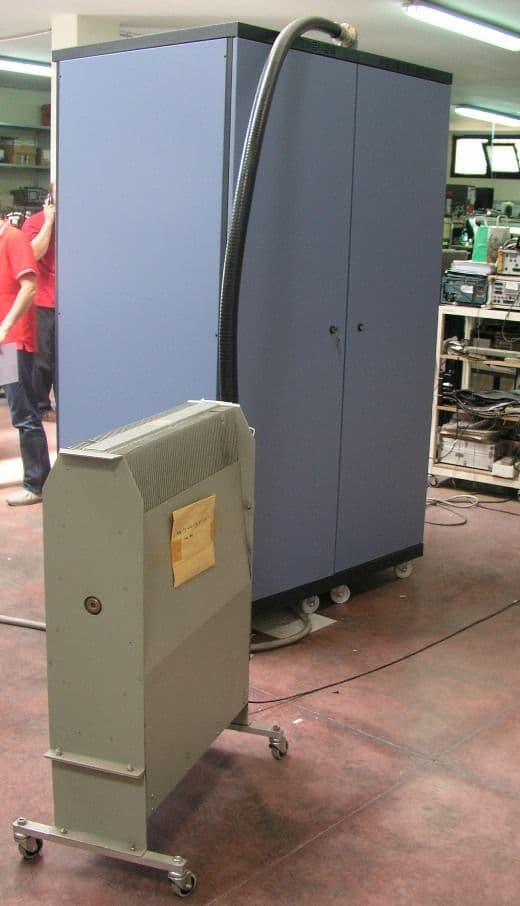
PHLTXUD3000A
Jun 17, 20103000 Watt ATSC Transmitter
Equipment Class
TBC - Licensed Broadcast Station Transmitter
PHLTXUD2000A
Jun 09, 20102000 Watt ATSC Transmitter
Equipment Class
TBC - Licensed Broadcast Station Transmitter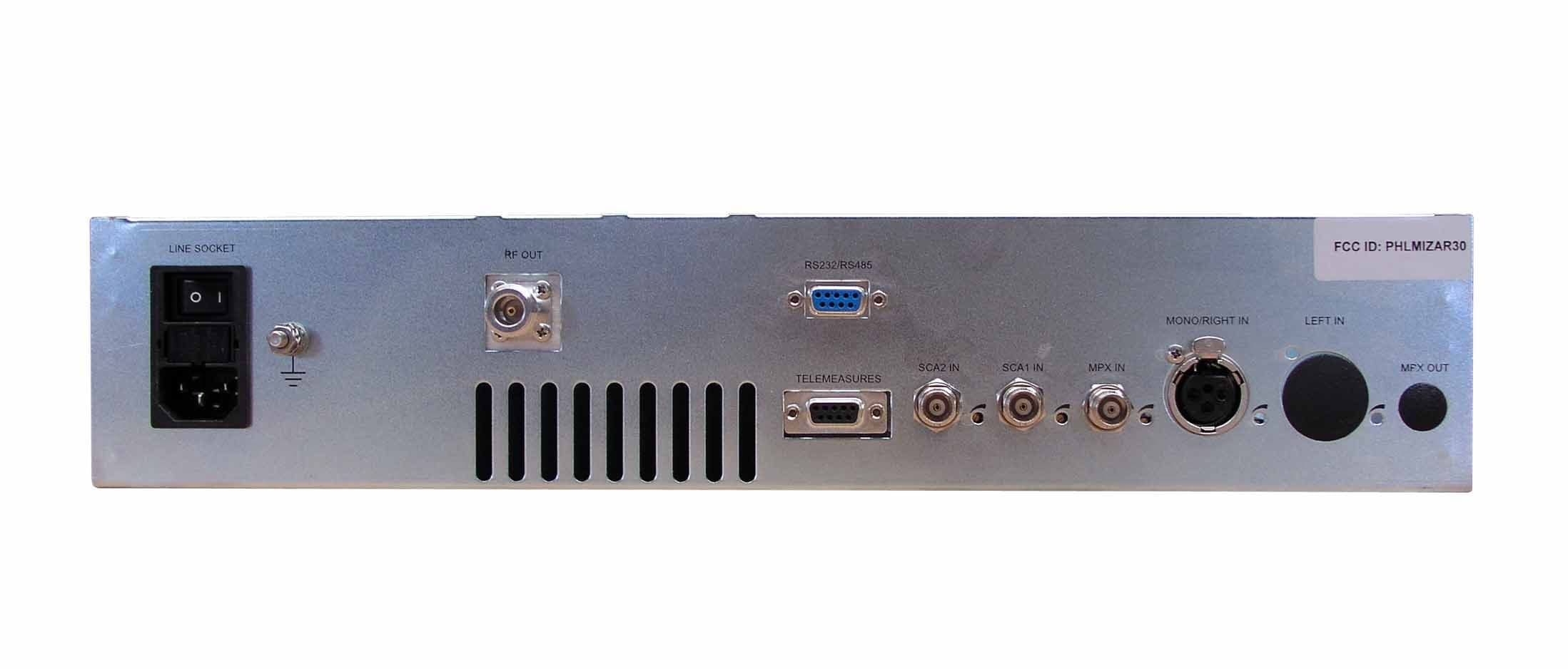
PHLMIZAR30
Jul 01, 200830 Watt FM Broadcast Transmitter
Equipment Class
TBC - Licensed Broadcast Station Transmitter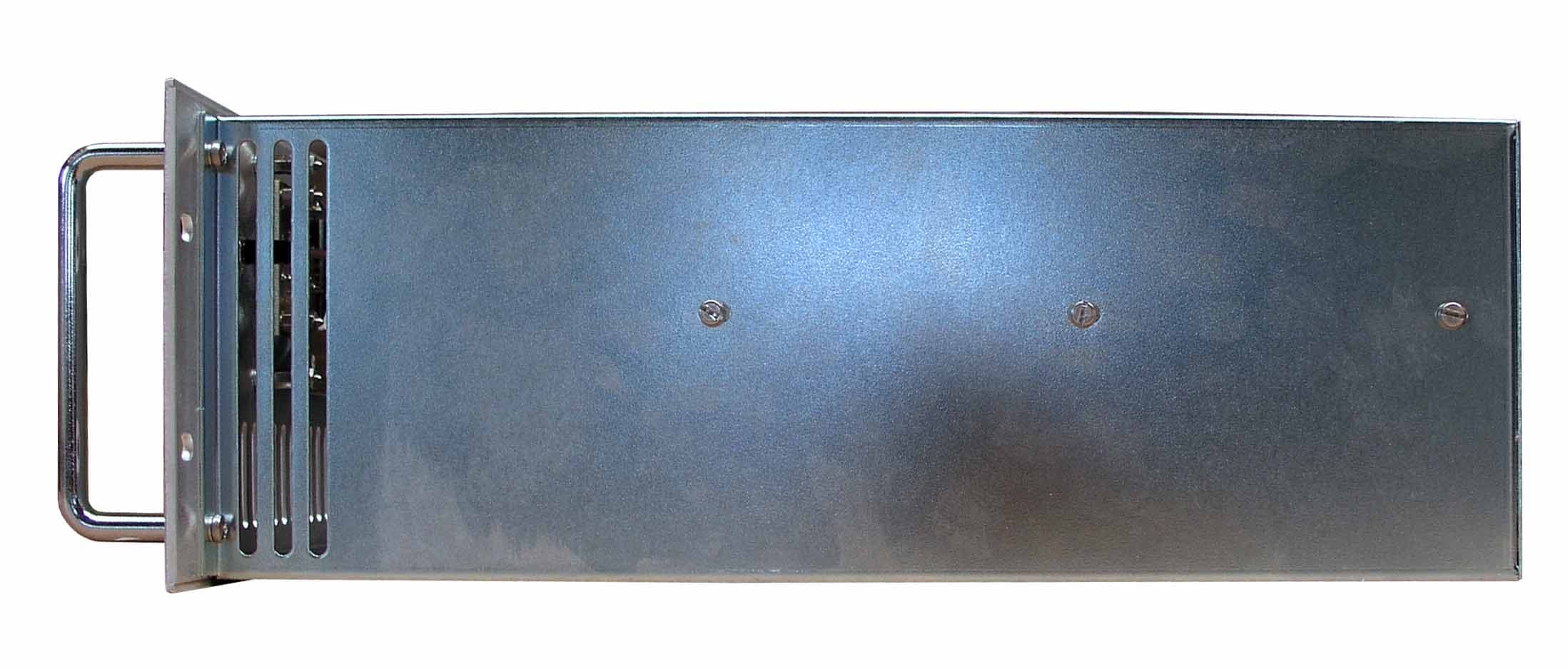
PHLMIZAR300
Jul 01, 2008300 Watt FM Broadcast Transmitter
Equipment Class
TBC - Licensed Broadcast Station Transmitter