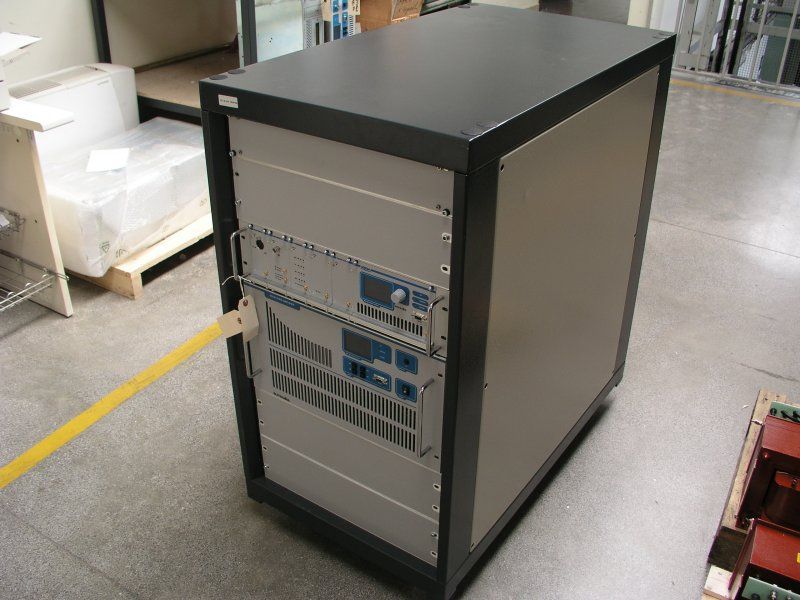
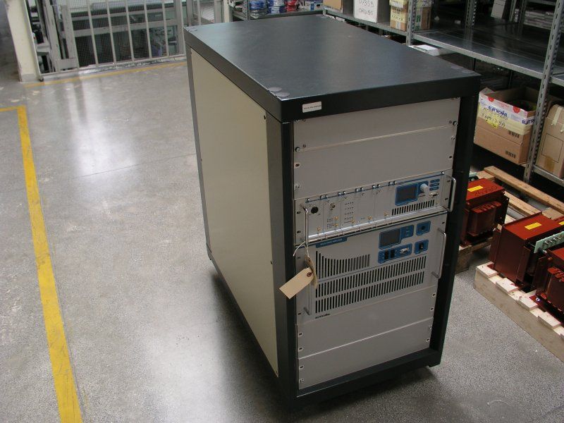
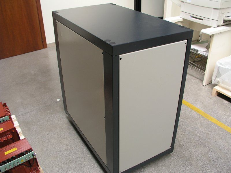
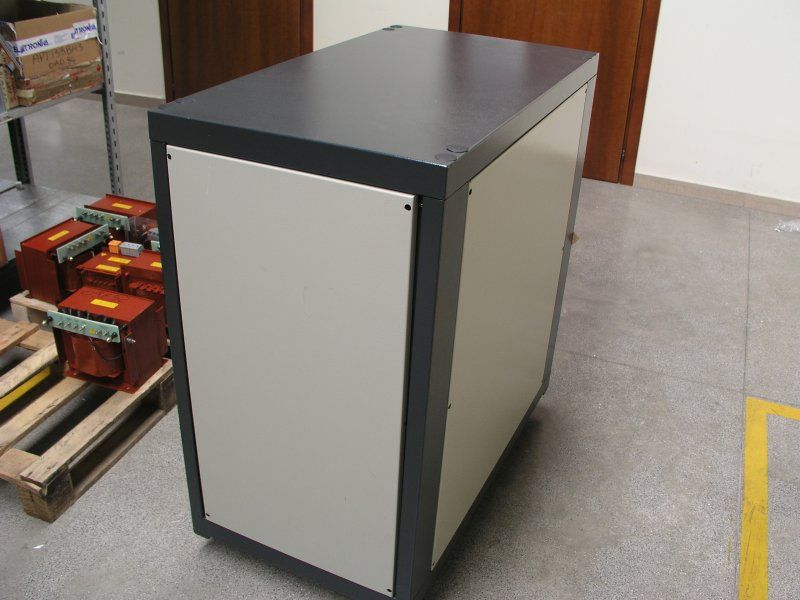
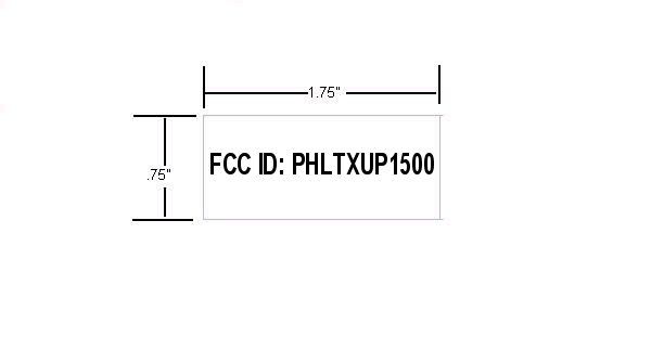
PHLTXUP15001300 Watt Analog TV Broadcast Transmitter
Elettronika S.r.l.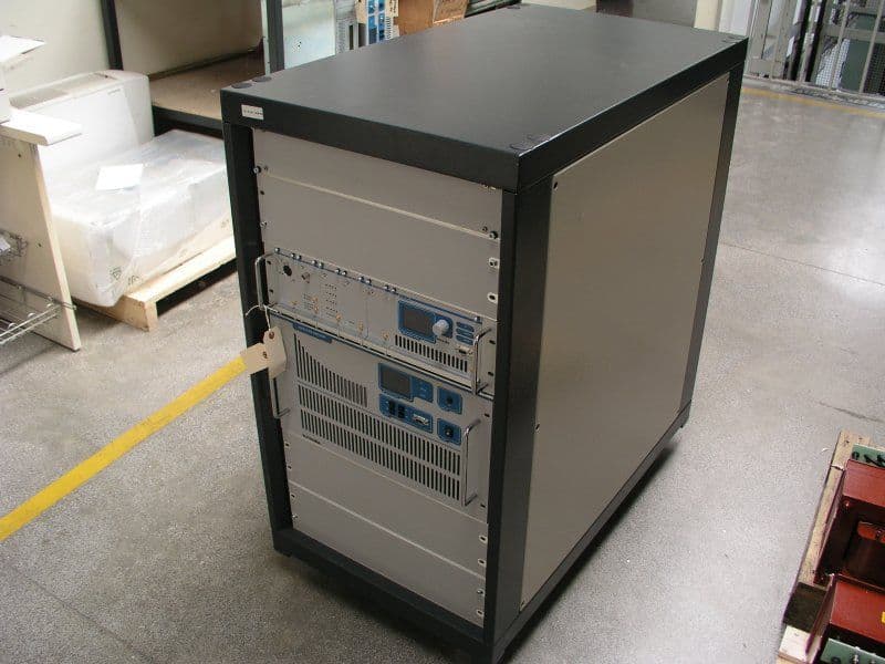
Click to zoom
Application Details
- Equipment Class
- TBC - Licensed Broadcast Station Transmitter
- Date of Grant
- Aug 03, 2006
- Application Purpose
- Original Equipment
- Date of Application
- Feb 19, 2006
- Equipment Note
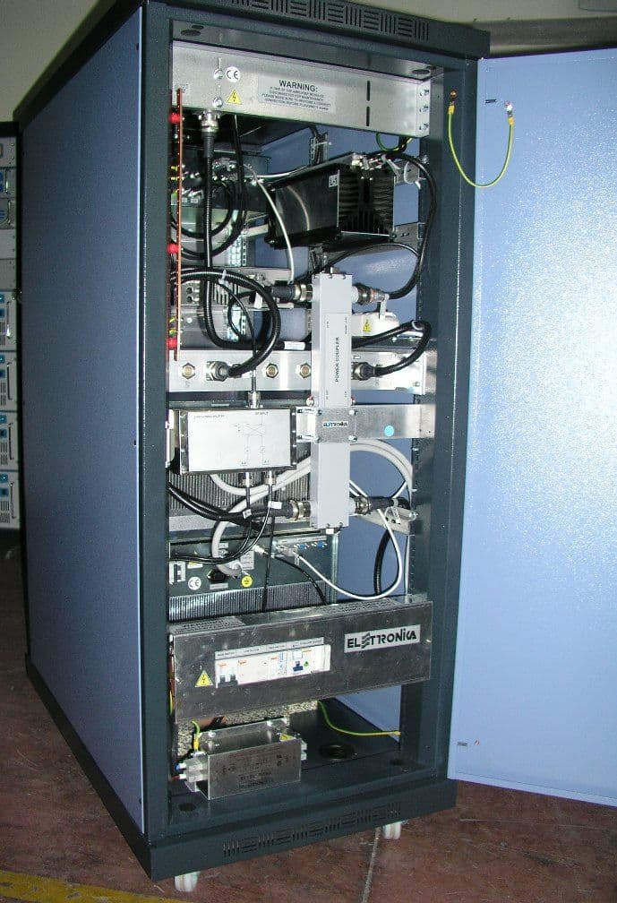
- 1300 Watt Analog TV Broadcast Transmitter
- Frequency Range
- 470.00000000 - 806.00000000
- Company
- Elettronika S.r.l.
- Country
- Italy
Documents & Files
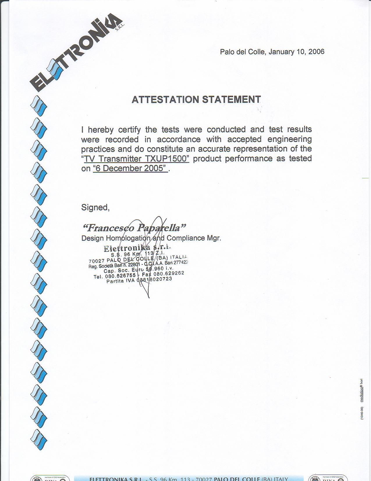
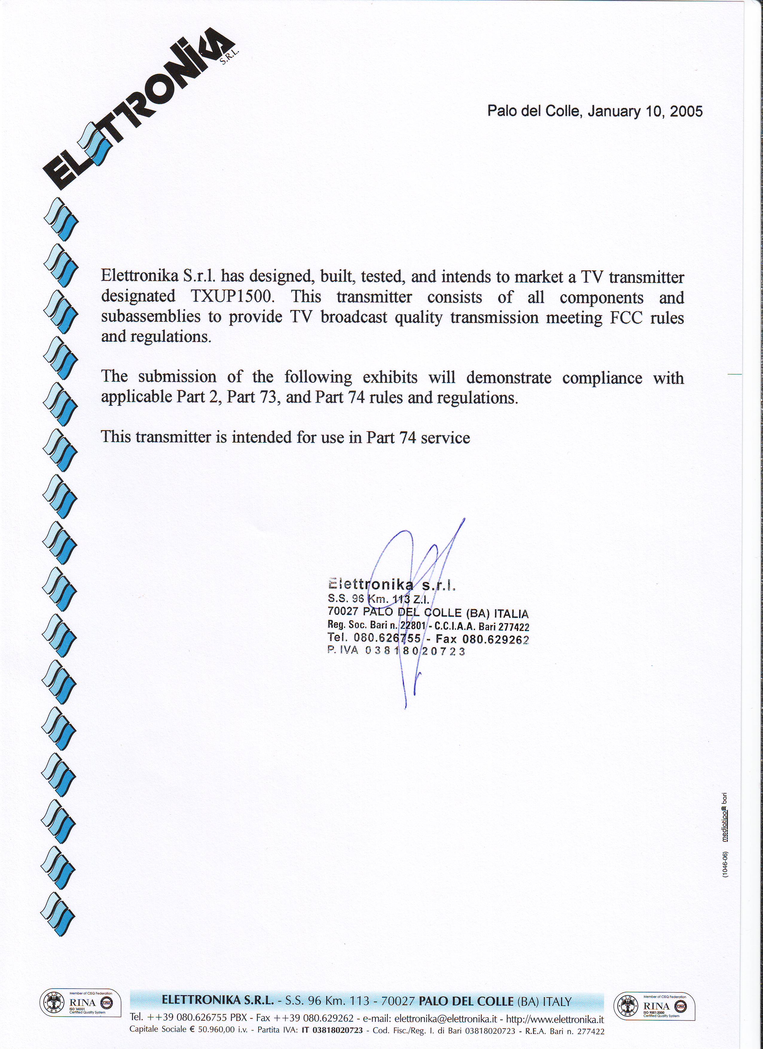
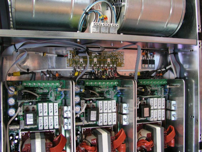
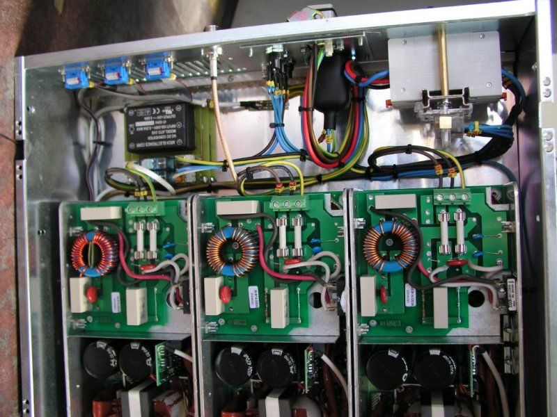
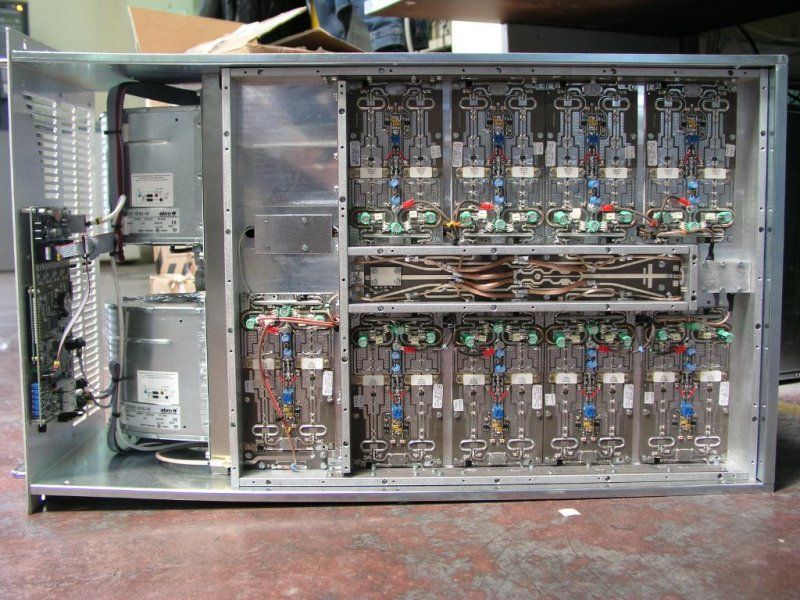
Document Text
Text extracted from the exhibit documents filed with the FCC. Open a document above to read the original.
Users Manual
VEGA UHF - TV System Userís manual CODE: APT139NM2 TITLE: VEGA REV: 0 DATE: 15/02/05 SS 96 Km 113 70027 Palo del Colle (Ba) ITALY Tel. +39 (0)80 626755 Fax +39 (0)80 629262 E-mail: [email protected] Web site: http://www.elettronika.it Registration number: IT-17686 Registration number: IT-24436 Index Index ................................................................................................................................... 3 Warning .............................................................................................................................. 5 Warranty ............................................................................................................................. 6 Introduction ....................................................................................................................... 7 Content of the manual....................................................................................................... 7 Treatment of electrical shock ........................................................................................... 9 First-aid ......................................................................................................................... 10 Treatment of electrical burns.......................................................................................... 10 Note ............................................................................................................................... 10 Section 1 - Information .................................................................................................... 13 1.1 Description............................................................................................................... 14 1.2 Main features ...........................................................................................................14 1.3 Technical characteristcs........................................................................................... 15 Front panel .................................................................................................................... 16 Rear panel ..................................................................................................................... 17 Section 2 - Installation..................................................................................................... 19 2.1 Menu management ................................................................................................. 20 2.2 Menu description ..................................................................................................... 22 - Multistandard Audio Mono Section .......................................................................... 22 - Multistandard Audio Stereo Section (Option) ........................................................... 25 - Multistandard Video Section .................................................................................... 29 - Multistandard IF Precorrector Section ...................................................................... 31 - Multistandard Local Oscillator Section with Line Offset ............................................ 32 - Multistandard Local Oscillator Section with Field Offset (Option) ............................. 34 - Multistandard Channel Filter Section ....................................................................... 36 - Controller Module Section ....................................................................................... 39 - RF Amplifier Module Section ................................................................................... 43 - BUS Structure Section ............................................................................................. 45 - External Reference Section ..................................................................................... 46 2.3 Alarms and automation............................................................................................ 48 2.4 External AGC: Implementation and details .............................................................. 50 2.5 Power handling ........................................................................................................ 53 2.6 VEGA Factory setting............................................................................................... 54 - Setup Configuration ................................................................................................... 55 Section 3 - Diagram ......................................................................................................... 57 Cable diagram ...............................................................................................................58 APT139NM2 VEGA - Component list ............................................................................... 59 MTG0071AR1 (Multistandard Audio Mono Modulator Module) .................................... 60 MTG0078AR0 (Multistandard Audio Stereo Modulator Module)................................... 67 MTG0072AR0 (Multistandard Video Modulator Module) .............................................. 76 MTG0073AR0 (Multistandard IF Precorrector Module) ................................................. 86 MTG0084AR0 (Multistandard UHF Local Oscillator Module) ..................................... 102 MTG0075AR0 (Multistandard UHF Channel Filter Module) ....................................... 108 MTG0079AR0 (Controller odule)................................................................................. 112 MTG0076AR0 (External Referement Module) ............................................................ 118 MTF0088BR0 (15W UHF Amplifier Module)............................................................... 122 SCH0194AR1 (BUS Structure).................................................................................... 130 E0017 (SP300-27 Switching power supply) ...................................................…
Text truncated - open the document above for the full version.
Users Manual
57 _______________________________________________________________________________________________ Section 3 - Diagram Contents: - Cable diagram - APT139NM2 VEGA Component list - Modules description 58 59 Part Name CodeDescriptionQty S0007MODULAR STRUCTURE1 MTG0077AR0POWER SUPPLY MODULE1 MTG0076AR0EXTERNAL REFEREMENT MODULE1 MTG0078AR0MULT. AUDIO STEREO MODULATOR - OPT.1 MTG0072AR0MULT. VIDEO MODULATOR MODULE1 MTG0073AR0MULT. IF PRECORRECTOR MODULE1 MTG0084AR0MULT. LOCAL OSCILLATOR MODULE1 MTG0075AR0MULT. CHANNEL FILTER MODULE1 MTG0079AR0DISPLAY AND POWER SUPPLY MODULE1 MTF0088BR015W UHF AMPLIFIER MODULE1 05352SAW FILTER SF0036BA01033T (EX 523) B/G1 OPT016OPTION NOTCH FILTER UHF VEGA1 S0007 VEGA Structure Part Name CodeDescriptionQty 05627BOARD GUIDE cod. 010Z00010 05616FRONT METAL SIDE M 2.5 cod. 000EA0842 05552B3-4U HANDLE KIT cod. 235.0122 DET1010DET1010R1 DOWN DIN GUIDE FOR VEGA1 05611AFRONT METAL SIDE cod. 000DA0842 05611BREAR METAL SIDE cod. 000DA0852 CON0256CON0256R0 LEFT SIDE FOR VEGA1 05609AANGULAR FOR HANDLE cod. 116ZF0012 05617REAR METAL SIDE M 2.5 cod. 000EA0852 SCH0194AR1BUS STRUCTURE1 05636APERFORATED COVER RACK cod. 405MB0842 0269910 WAYS FEMALE CONNECTOR cod. IDS10FSR14 0286720 CONT. FEMALE CONNECTOR cod. IDS20FSR14 028846 WAYS MALE KSC 6 EXTR. CLAMP-HOLDER2 028814 WAYS MALE KSC 4 EXTR. CLAMP-HOLDER2 028972 WAYS MALE 90∞ KSCO2 EXTR. CLAMP-HOLDER 1 VEN00004PAPST FAN mod. 4184NXH 24V1 07596FAN GRID LZ 2011 DET0875IDET0875R1 CONVEYER FAN FOR VEHA INOX P.2678 1 CON0239CON0239R0 RIGHT SIDE FOR VEGA1 08878RG316 50W 41626-SMB 90∞ 260mm DIN CABLE1 08879RG316 50W 41626-SMB 220mm DIN CABLE2 08880RG316 50W 41626-41626 120mm CABLE3 DET1056DET1056R1 UP DIN GUIDE FOR VEGA1 02513SMB 90∞ R114186000 SOCKET1 02515SMB R114313000 SOCKET1 08502RG316 50W CABLE1 Component listAPT139NM2 - VEGA 60 MULT. AUDIO MONO MODULATOR MODULEMTG0071AR1 DESCRIPTION The audio signal enters the module through one 600W balanced or 10kW unbalanced XLR connection, which may be placed either on the front or rear panel and software- selected. It is conditioned by a digital power-meter with a ±8dB 0.5dB-step dynamic and muting. Then there are the emphasis and clipping stages (which can be inserted via software), before the frequency modulation of the audio carrier. The control system of the audio subcarrier is a PLL which locking frequency can be selected via software depending to the transmission standard, while the reference frequency comes from the video module. The control frequency comes from a VCTCXO inside the module to foresee the possibility of a separated-audio system, for which the 20MHz may be locked to a more precise system coming from the 5/10MHz bus. The carrier obtained this way is modulated in frequency and level-conditioned by an IF gain stage trough a digital power-meter with a ±3dB dynamic in fine tuning before being added to the video carrier. The following control signal for the modulator operation are present on the board: PLL lock status of the audio subcarrier, Overload on the audio input, Peak level of the deviation of the audio subcarrier. All of the operating parameters of the board are managed by the built-in micro-processor. Communication to outside are performed trough RS485 bus. TECHNICAL CHARACTERISTICS Input impedance600W - 10kW selectable Nominal level2Vpp -•/+8dB InputFront and back XLR selectable EmphasisFLAT-50msec (FLAT-75usec) Deviation limiterSelectable Low-pass filter15kHz excludible Frequency response< ±0.5dB THD< 0.5% Intermodulation< 60dB (d2,d3) Synchronous AM S/N> 50dB Asynchronous AM S/N> 70dB FM S/N CCIR> 72dB Analog measuresCarrier FM deviation Carrier frequency synthesisPLL Audio carrier characteristicsOn/Off selection and level adjustment > ±3dB Frequency referenceInternal TCXO externally lockable External interfaceMicroprocessor with RS485 protocol FirmwareRe-configurable through RS485 61 62 The module contains the following blocks: 1. Input relay ñ chooses the audio source between the XLR on the front panel of the module and the one on the back of the apparatus and selects the input impedance to 600W or 10kW; both switching are managed by the software. 2. Audio level regulation stage ñ regulates the level of the audio signal by means of a digital potentiometer which can be programmed trough a uWIRE interface (with 0.5dB step between -8dB and +8dB). 3. Emphasis stage ñ inserts an emphasis curve on the audio signal with a time constant depending on the standard (50,75us); the choice can be selected via software. 4. Deviation limiter ñ cuts the audio level to limit the FM deviation; its intervention is handled by the software and the intervention of the clipper, if any, is signalled by a red LED on the front panel. 5. Low-pass filter ñ filters the audio signal before the modulation to suppress external residues from the audio band (20Hz-15kHz); the filter can be inserted by means of jumpers on the board. 6. Audio signal level measurement ñ this stage detects the peak level of the audio signal providing a conditioned analog voltage for the A/D conversion; the voltage will be processed by the microcontroller of the display board (see MTG0079) to be shown as VU-METER. 7. Frequency modulator ñ converts to intermediate frequency the audio signal as FM modulation of a carrier. 8. Carrier level regulation stage ñ switches on and off the audio carrier and the regulation within at least ±3dB of the level referring to the video carrier. 9. IF amplifier ñ amplifies the audio carrier to obtain an output level of -6dBm. 10. Output low-pass filter ñ filters the harmonics of the audio carrier. 11. Audio IF oscillator ñ generates the audio carrier performing the PLL frequency synthesis; the selectable standards and the lock indication are handled by the software. 12. 20MHz reference ñ the frequency reference for the PLL synthesis of the carrier is generated by a TCXO which may be locked to a more precise 5/10MHz external reference (see MTG0076). 13. Controller ñ all of the described…
Text truncated - open the document above for the full version.
Users Manual
102 MULT. UHF LOCAL OSCILLATOR MODULEMTG0084AR0 DESCRIPTION The synthesis system of the local oscillator for the channel conversion is based on a control technique which allows to obtain the programming of the standard, the channel (split into the three bands I, III, IV/V) and the line offset (as multiple of the line frequency of the video signal) via software, with no change to be made. The module includes an internal VCTCXO reference which can be locked to a more precise 5/10MHz reference (trough the bus) needed if the field offset is used. TECHNICAL CHARACTERISTICS Nominal level+13dBm ±1dB FM S/N ccir unweight.> 65dB FM S/N ccir wght.> 60dB Analog measuresVCO control voltage Carrier frequency synthesisA PLL OffsetLine offset, step ±1/12 line frequency O.L. carrier characteristicsOn/Off selection and fine adjust Frequency referenceInternal TCXO externally lockable External interfaceMicroprocessor with RS485 protocol FirmwareRe-configurable via RS485 103 104 The module contains the following blocks: 1. Local oscillator ñ generated the carrier to be synthesised, it is split into three windows (I-II / III / IV-V band) to ensure the coverage of all of the TV channels to be implemented for all standards. 2. Radio-frequency splitter ñ splits the signal coming from the local oscillator by means of splitters and amplifiers, with 10dB attenuation and gain respectively, to ensure the complete isolation of the LO from the other stages and to minimise the ëfrequency pullingí phenomenon. 3. PLL stage ñ synthesises the desired channel by locking the LO to a 20MHz frequency reference by means of a PLL which can be configured via uWire and provides the locking and line-offset indication (LED on frontal panel); the choice is made via software. 4. Active ring filter ñ stabilises the system in PLL retro-action and e has to be modified if the operating band of the module changes (see table attached to the electrical diagram). 5. Conditioning stage of the correction voltage ñ conditions the correction voltage of the PLL ring providing a conditioned analog voltage for the A/D conversion; the voltage is processed by the microcontroller of the display board (see MTG0079) to be displayed as VU-METER. 6. Mixer ñ in the UPCONVERTER version of the module, converts to channel the intermediate frequency coming from the pre-corrector (see MTG0073) using a LEVEL13 mixer (in case the module is only used as LO, see REPEATER configuration, this stage is not present and the synthesised carrier goes directly to the output of the module). 7. 20MHz reference ñ the frequency reference to the PLL synthesis of the carrier is generated by an internal TCXO which fine control of the frequency is internally generated via PWM by the microcontroller or, alternately, can be locked to a more precise 5/10MHz external reference (see MTG0076). 8. Controller ñ all of the described operations are managed by a microcontroller communicating to the user interface board (see MTG0079) by RS485 protocol; the local controller stores the status of the module and a reprogramming of the firmware (possible via RS485 from the display board) does not alter its contents. CALIBRATION PROCEDURE - List of instrument MEASUREINSTRUMENT Lock of the carriers and reference - Spectrum analyser - Oscilloscope - Tester 105 The calibration procedure of the module requires a complete structure of display board (see MTG0079) and extension module (see MTG0095) in order to perform the software selection which will be referred to later and power the module itself.. - Menu of the Multistandard UHF Local Oscillator Module Verification of the local oscillator section ñ connect a spectrum analyser to the monitor of the J4 module and check the sections therein: qConfigure the module with Output Enabled, LineOffset Zero, Ref Internal and Channel on the desired channel, and calibrate C1(C2 and C3) to lock the carrier to the LO frequency of the standard and channel set (to change the standard refer to the standard changing procedure) and obtain a locking voltage between 2V and 3V on TP1, checking that VCO is on Lock in the display menu. Verification of the external reference section ñ connect a spectrum analyser to the monitor of the J4 module and check the sections therein: qConfigure the module with Ref Internal and check that it is possible to find adjust the synthesised frequency by acting on Tune. - Description of the adjustment points COMPONENTDESCRIPTION C1, C2, C3 Tuning of the local oscillator (SCH0292 - 0309 - 0310) J3 LO input J5, J8 RF link (absent in case of LO configuration) J4 LO monitor (panel) JP1 Unused J2 Testpoint for the debug of the PLL 106 Component layout for adjustment points 107 Component layout SCH0293AR0 Component layout SCH0292AR0 108 MULT. UHF CHANNEL FILTER MODULEMTG0075AR0 DESCRIPTION The module filters the signal coming from the conversion mixer removing the local oscillator and the upper side-band and contains the voltage-controlled gain stage composed by a pin-diode attenuation cell followed by a wide-band amplification stage used as driver of the final stage. TECHNICAL CHARACTERISTICS Input/output impedance 50W R.O.S.>20dB Filter type Active 5-cell band-pass RF-attenuation type 4 PIN-diodes cell Output amplifier Wide band Overall gain 25dB (max.) The module contains the following blocks: 1. Active band-pass filter ñ filters the lower side-band after conversion, it is split into three windows (I-II / III / IV-V band) to ensure the coverage of all of the TV channels to be implemented for all standards, and contains the PIN-diode attenuation cell for the gain control. 2. Wide-band amplifier ñ amplifies the filtered channel in order to obtain the correct driving level for the RF final stages (see MTF0088-0087-0089). CALIBRATION PROCEDURE - List of instruments MEASUREINSTRUMENT Calibration of the channel filter - Network analyser - Spectrum analyser with tracking 109 The calibration procedure of the module requires a complete structure of display …
Text truncated - open the document above for the full version.
Users Manual
AUTV/1500LD LDMOS - UHF TV Solid State Amplifier Userís manual CODE: APT144DM TITLE: AUTV/1500LD REV: 0 DATE: 04/05/05 SS 96 Km 113 70027 Palo del Colle (Ba) ITALY Tel. +39 (0)80 626755 Fax +39 (0)80 629262 E-mail: [email protected] Web site: http://www.elettronika.it Registration number: IT-17686 Registration number: IT-24436 Index Index ................................................................................................................................... 3 Warning .............................................................................................................................. 5 Warranty ............................................................................................................................. 6 Introduction ....................................................................................................................... 7 Content of the manual....................................................................................................... 7 Treatment of electrical shock ...........................................................................................9 First-aid ......................................................................................................................... 10 Treatment of electrical burns.......................................................................................... 10 Note ............................................................................................................................... 10 Section 1 - Information .................................................................................................... 13 1.1 Description............................................................................................................... 14 1.2 Technical characteristics.......................................................................................... 15 Section 2 - Installation..................................................................................................... 17 2.1 Operating environment ............................................................................................ 18 2.2 Preliminary operations............................................................................................. 18 2.3 Telemeasuring socket connections ......................................................................... 19 2.4 RS232, RS485 and AGC Socket connections ......................................................... 19 2.5 Preventive maintenance .......................................................................................... 20 Front panel .................................................................................................................... 21 Rear panel ..................................................................................................................... 22 Section 3 - Operation....................................................................................................... 23 3.1 Operation ................................................................................................................. 24 3.2 Display..................................................................................................................... 25 3.3 Menu........................................................................................................................ 25 - RF Powers ................................................................................................................ 27 - Power Supply ........................................................................................................... 27 - Log/Alarms............................................................................................................... 27 - Working timer ........................................................................................................... 28 - Thresholds ............................................................................................................... 28 - RMS/Peak................................................................................................................ 29 - Date/Time ................................................................................................................ 29 - Display ..................................................................................................................... 29 - Frequency (only for FM Amplifiers) .......................................................................... 30 - Slave address .......................................................................................................... 30 - Remote .................................................................................................................... 30 - Interlock.................................................................................................................... 30 - Firmware release......................................................................................................31 - Serial number .......................................................................................................... 31 Section 4 - Diagram ......................................................................................................... 33 Cable diagram ...............................................................................................................34 MTF0070CR0 RF Amplifier module Cable Diagram .................................................... 35 MTF0070CR0 RF Amplifier module Connections Diagram.......................................... 36 MTF0070CR0 Amplifier module - Component list ........................................................ 37 APT144A AUTV/1500LD - Component list ....................................................................... 39 SCH0192AR0 (200W UHF LDMOS Amplifier module) ................................................ 41 - Calibration procedure...................…
Text truncated - open the document above for the full version.
Users Manual
33 _______________________________________________________________________________________________ Section 4 - Diagram Contents: - Cable diagram - MTF0070CR0 RF Amplifier module Cable Diagram - MTF0070CR0 RF Amplifier module Connections Diagram - MTF0070CR0 Amplifier module - Component list - SCH0192AR0 (200W UHF LDMOS Amplifier module) - SCH0223AR1 (Control board and display) - SCH0221AR1 (Amplifier interface) - SCH0265AR0 (Mains distribution board) - SCH0288AR1 (Interface board) - E0012 (SP500-27-DI Switching power supply) 34 35 36 37 Part Name CodeDescriptionQty 000010W 1206 SMD RESISTOR2 01041D1nF 1206 2% SMD CAPACITOR2 00221B75W 1206 1% SMD RESISTOR2 03207HSMS-2802*L31 DIODE2 SCH0192AR0200W UHF LDMOS AMPLIFIER MODULE9 SCH0221AR0AMPLIFIER INTERFACE1 SCH0248AR08 WAY WILKINSON1 SCH0249AR04 WAY WILKINSON Dx1 SCH0250AR04 WAY WILKINSON Sx1 SCH0251AR02 WAY WILKINSON1 SCH0252AR01500W UHF INPUT COUPLER1 PN1091AC.S. PN1091AR3 OUTPUT DIRECTIONAL COUPLER 1 024027/16î FEMALE CONNECTOR cod. 01421 02512J01151A0531 SMA SOCKET WITHOUT BAT.1 014002499-003-X5U0-102M FEED-THROUGH CAPACITOR 13 014085000PF FEED-THROUGH CAPACITOR2 DET0726DET0726R2 SIDE x 1500W UHF AMP. MOD.2 DET0727DET0727R1 INTERNAL FRONT SIDE x AMP. MOD. 1 DET0728DET0728R4 INTERNAL SIDE x AMP. MOD.2 DET0729DET0729R2 FRONT SIDE x AMP. MOD.1 DET0730DET0730R2 REAR SIDE x AMP. MOD.1 DET0732DET0732R1 CONNECTIONS SUPPORT BOARD1 DET0734DET0734R0 COVER x AMPLIFIER MODULE P. 2634 1 DET0736DET0736R6 HEATSINK x AMPLIFIER MODULE1 DET0807DET0807R3 SCREEN DIR. COUPLER MODULE1 DET0810DET0810R0 PART. x DIRECTIONAL COUPLER1 DET0811DET0811R1 COVER x DIRECTIONAL COUPLER1 DET0812DET0812R1 TEFLON RING x DIRECTIONAL COUPLER 1 DET0819DET0819R0 SPESS. x INPUT DIR. COUPLER1 DET0828DET0828R0 COVER x AMPLIFIER MODULE P. 2644 1 DET0839DET0839R2 DIRECTIONAL COUPLER1 08502RG316 50W CABLE3,00 08527HF-85 ENDIFORM CABLE0,20 03017MBR3045PT DIODE4 PN0998APN998AR1 POWER SUPPLY ADDED PCB2 Component listMTF0070CR0 Amplifier module 38 This page is intentionally blank 39 Part Name CodeDescriptionQty 05553BKIT MANIGLIE 5-6U cod. 235.0132 V0962MORSETTIERA/GIUNZIONE ELECO E8062 V0760TAPPI NERI 0 9.5 PLASTICA DP-3751 SCH0223AR1CONTROL BOARD AND DISPLAY1 SCH0265AR0MAINS DISTRIBUTION BOARD1 MTF0070CR0RF AMPLIFIER MODULE1 09419C.S. PN419/A SUPPOR. SENSORE TEMPER.1 PN1114AC.S. PN1114AR1 SCHEDA CABL. VENT. x 1kW III1 07925PROTEZIONE IN GOMMA PVC PG 0751 07515CINTER. AUTOM. 4P*16A 4.5KA 2 mod. GW 900871 07524AINTERR. NERI I39101 07541PORTAFUS. 10A PANN. cod. P18203 02830PRESA VDE 10A cod. PX675 A631 02893MORSETTIERA ESTRA. 3VIE MAS. KSC 33 02894MORSETTIERA ESTRA. 3 VIE FEM. KB 33 02695CONNETTORE DB9F x CAVO IU0080593 02699CONNETTORE cod. IDS10FSR1 FEMM. 10 VIE9 02700CONNETTORE cod. IDS16FSR1 FEM. 16 VIE1 02228GE 15145 D/60 NF A VITONE1 02502J01150A0041 SMA x RG58/c1 02876PRESA VOLANTE ILME 16A PENTAPOLARE 4MT 1 02877SPINA A PANNELLO ILME 16A 5P 35cm1 07605ACOND. 2uF2 07605BVENTOLA D2E097-BI56-482 07605FGRIGLIA 09485-2-40394 010411nF COND. CERAMICO 50V2 00664SENSORE TERMICO LM 35DT1 FUS1AFUSIBILI 1A 5x20 RITARDATI ST5202101 FUS3AFUSIB. 3.15A 5x20 RITAR. ST5202311 FUS5AFUSIBILI 5A 5x20 RITARDATI ST5202501 CON0171CON0171R5 SOST. VENT. 1kW LDM. PH. ZN P.2614 1 CON0178CON0178R4 POST. 1500W LDMOS UHF ZN1 DET0516DET0516R0 SUPPORTO PRESE ZN P.26421 DET0772DET0772R0 BARRETTA FISSAGGIO VENTOLE2 Z0021TONDO IN OTTONE x INT. MAGNET. TAV. 635/A2 Z0081SUPPORTO GUIDA DIN INT. MAG.1 Z0673TAV. 1199 CHIUS. CONT. PROF. 775 ZN P.23662 E0012SP-500-27 DE2 SWITCHING POWER SUPPLY8 PAN0074PAN0074AR2 PANN. 6U AMPLIFICATORE LDMOS 1 08503CABLE RG303 50W TEFLON1,20 DET0575DET0575R1 BARRA FISSAGGIO ALIM. SP-5008 SCH0288AR2INTERFACE BOARD1 CON0237CON0237R2 LAT. SX 1500W UHF MW P.2743 ZN1 CON0238CON0238R1 LAT. DX 1500W UHF MW P.2744 ZN1 DET0996DET0996R0 BARRA FISS. SCHEDA DISTR. RETE1 DET0995DET0995R0 BARRA FISSAGGIO ALIM. SP-5001 Component listAPT144A - AUTV/1500LD 40 This page is intentionally blank 41 200W UHF LDMOS AMPLIFIER MODULESCH0192AR0 DESCRIPTION The RF module is an integrated TV linear amplifier designed for UHF band, this module employs push-pull LDMOS technology in order to achieve very good efficiency, high linearity and reliability. LDMOS transistors operate in AB class. It is a wideband amplifier over the full frequency, no adjustment is required for the channel change. The board includes RF section amplifier, bias circuit, protection circuit and matching networks. A silver plated copper plate is brazed with PCB in order to obtain low thermal resistance. Providing a minimum of 200W Pk sync linear power, this module is the perfect amplifier for any broadband UHF power transmitter. TECHNICAL CHARACTERISTICS Output power300W max Input power15W max Frequency470 - 860MHz Gain> 13dB LDMOS Power supply32V ±2% LDMOS Bias current @+32V Vdc 2A RF Input impedance50W RF Output impedance50W Input / Output return loss> = 15dB Drain efficiency47% @ 250W Storage temperature range-50∞ to +150∞C Dimensions (LxWxH)165x95x29mm 42 CALIBRATION PROCEDURE - Technical characteristics Power supply voltage32V (± 2%) Polarisation current1.0 cold for each device (2A total), ± 0.1A Gain for low signalNot less than 13dB in the 470-860MHz band (± 1dB) Compare to the typical curve eclosed - Adjustment procedure Polarisation current calibration32V stabilised power supply 10A amperometer Gain curveNetwork analyser - Adjustment points description R7-R8 (Trimmers)Adjust the current absorbed in stand-by (1.0A per device) Middle frequency 660MHz, span 500MHz, 2dB/div., reference to the arrow - Curve response graphic 43 - Calibration steps STEP 1.Close the input and the output of the module by connecting them to a 50 WW WW W dummy load and connect the spectrum analyser through a directive sample, in order to look for self-oscillation of the module, if any (anyway the module has been designed so that it would not self-oscillate even if totally de- coupled, without any input or output load). STEP 2.Check the voltages of the polarisation circu…
Text truncated - open the document above for the full version.
Contact Information
Applicant
Francesco Paparella(Design Omologation and Compliance Mgr)
Technical Contact
Greg Best Consulting, Inc.Greg Best
[email protected]816-792-2913
9223 N. Manning Avenue · Kansas City, Missouri · United States
Technical Specifications
| # | Rule Parts | Frequency Range | Power Output | Emission | Tolerance |
|---|---|---|---|---|---|
| 2 | 74 | 470 MHz - 806 MHz | 130 W | 250KF3E | 1000 Hz |
Other Applications from Elettronika S.r.l.
PHLTXUD1000A
Jul 07, 20101000 W ATSC Transmitter
Equipment Class
TBC - Licensed Broadcast Station Transmitter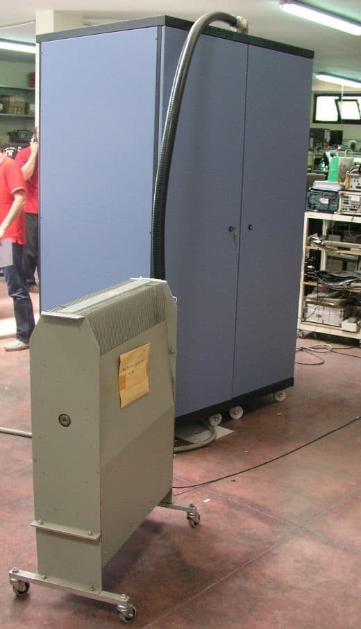
PHLTXUD3000A
Jun 17, 20103000 Watt ATSC Transmitter
Equipment Class
TBC - Licensed Broadcast Station Transmitter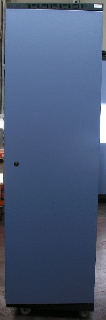
PHLTXUD2000A
Jun 09, 20102000 Watt ATSC Transmitter
Equipment Class
TBC - Licensed Broadcast Station Transmitter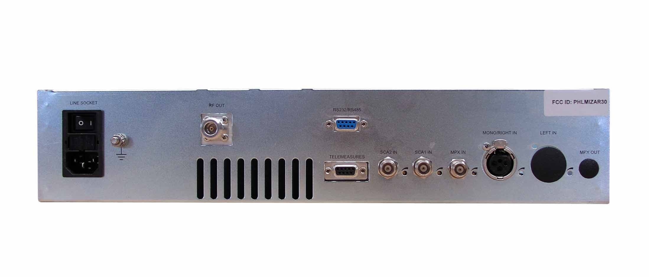
PHLMIZAR30
Jul 01, 200830 Watt FM Broadcast Transmitter
Equipment Class
TBC - Licensed Broadcast Station Transmitter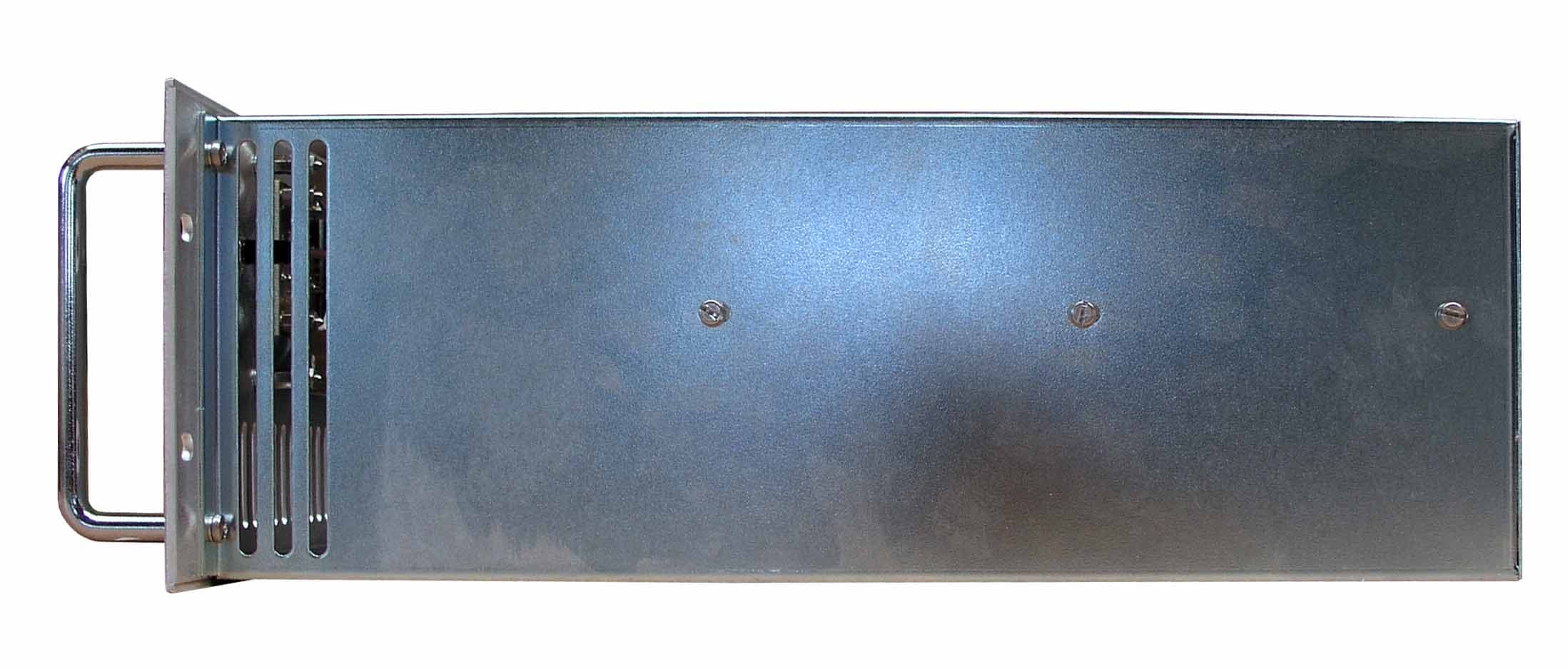
PHLMIZAR300
Jul 01, 2008300 Watt FM Broadcast Transmitter
Equipment Class
TBC - Licensed Broadcast Station Transmitter