PHLTXUP35003.5 kW Analog TV Broadcast Transmitter
Elettronika S.r.l.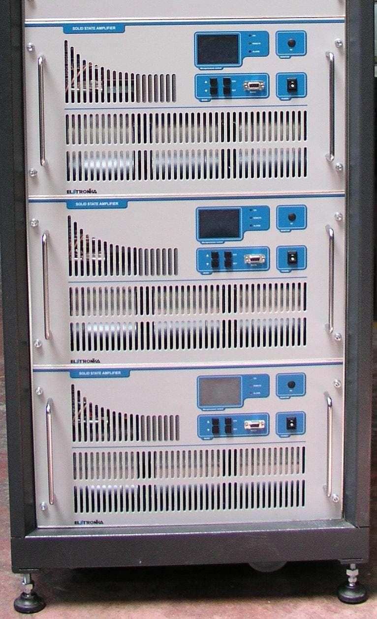
Click to zoom
Application Details
- Equipment Class
- TBC - Licensed Broadcast Station Transmitter
- Date of Grant
- Jan 30, 2007
- Application Purpose
- Original Equipment
- Date of Application
- Dec 03, 2006
- Equipment Note
- 3.5 kW Analog TV Broadcast Transmitter
- Frequency Range
- 614.00000000 - 806.00000000
- Company
- Elettronika S.r.l.
- Country
- Italy
Documents & Files

Document Text
Text extracted from the exhibit documents filed with the FCC. Open a document above to read the original.
Users Manual
AUTV/3500LD LDMOS - UHF TV Solid State Amplifier Userís manual CODE: APT137BM TITLE: AUTV/3500LD REV: 0 DATE: 09/06/05 SS 96 Km 113 70027 Palo del Colle (Ba) ITALY Tel. +39 (0)80 626755 Fax +39 (0)80 629262 E-mail: [email protected] Web site: http://www.elettronika.it Registration number: IT-17686 Registration number: IT-24436 Index Index ................................................................................................................................... 3 Warning .............................................................................................................................. 5 Warranty ............................................................................................................................. 6 Introduction ....................................................................................................................... 7 Content of the manual....................................................................................................... 7 Treatment of electrical shock ...........................................................................................9 First-aid ......................................................................................................................... 10 Treatment of electrical burns.......................................................................................... 10 Note ............................................................................................................................... 10 Section 1 - Information .................................................................................................... 13 1.1 Description............................................................................................................... 14 1.2 Technical characteristics.......................................................................................... 15 Section 2 - Installation..................................................................................................... 17 2.1 Operating environment ............................................................................................ 18 2.2 Preliminary operations............................................................................................. 18 2.3 Telemeasuring socket connections ......................................................................... 19 2.4 RS232, RS485 and AGC Socket connections ......................................................... 19 2.5 Preventive maintenance .......................................................................................... 20 Front panel .................................................................................................................... 21 Rear panel ..................................................................................................................... 22 Section 3 - Operation....................................................................................................... 23 3.1 Operation ................................................................................................................. 24 3.2 Display..................................................................................................................... 25 3.3 Menu........................................................................................................................ 25 - RF Powers ................................................................................................................ 27 - Power Supply ........................................................................................................... 27 - Log/Alarms............................................................................................................... 27 - Working timer ........................................................................................................... 28 - Thresholds ............................................................................................................... 28 - RMS/Peak................................................................................................................ 29 - Date/Time ................................................................................................................ 29 - Display ..................................................................................................................... 29 - Frequency (only for FM Amplifiers) .......................................................................... 30 - Slave address .......................................................................................................... 30 - Remote .................................................................................................................... 30 - Interlock.................................................................................................................... 30 - Firmware release......................................................................................................31 - Serial number .......................................................................................................... 31 Section 4 - Diagram ......................................................................................................... 33 Cable diagram ...............................................................................................................34 AUTV/1500LD Component layout ................................................................................. 35 RF section Block Diagram............................................................................................. 36 MTF0070BR0 Amplifier module - Component list ............................................................ 37 APT117B AUTV/1500LD - Component list ....................................................................... 39 SCH0192AR0 (200W UHF LDMOS Amplifier module) ................................................ 41 …
Text truncated - open the document above for the full version.
Users Manual
73 _______________________________________________________________________________________________ Section 4 - Diagram Contents: - Cable diagram - MTF0070CR0 RF Amplifier module Cable Diagram - MTF0070CR0 RF Amplifier module Connections Diagram - MTF0070CR0 Amplifier module - Component list - SCH0192AR0 (200W UHF LDMOS Amplifier module) - SCH0223AR1 (Control board and display) - SCH0221AR1 (Amplifier interface) - SCH0265AR0 (Mains distribution board) - SCH0288AR1 (Interface board) - E0012 (SP500-27-DI Switching power supply) 74 75 76 77 Part Name CodeDescriptionQty 000010W 1206 SMD RESISTOR2 01041D1nF 1206 2% SMD CAPACITOR2 00221B75W 1206 1% SMD RESISTOR2 03207HSMS-2802*L31 DIODE2 SCH0192AR0200W UHF LDMOS AMPLIFIER MODULE9 SCH0221AR0AMPLIFIER INTERFACE1 SCH0248AR08 WAY WILKINSON1 SCH0249AR04 WAY WILKINSON Dx1 SCH0250AR04 WAY WILKINSON Sx1 SCH0251AR02 WAY WILKINSON1 SCH0252AR01500W UHF INPUT COUPLER1 PN1091AC.S. PN1091AR3 OUTPUT DIRECTIONAL COUPLER 1 024027/16î FEMALE CONNECTOR cod. 01421 02512J01151A0531 SMA SOCKET WITHOUT BAT.1 014002499-003-X5U0-102M FEED-THROUGH CAPACITOR 13 014085000PF FEED-THROUGH CAPACITOR2 DET0726DET0726R2 SIDE x 1500W UHF AMP. MOD.2 DET0727DET0727R1 INTERNAL FRONT SIDE x AMP. MOD. 1 DET0728DET0728R4 INTERNAL SIDE x AMP. MOD.2 DET0729DET0729R2 FRONT SIDE x AMP. MOD.1 DET0730DET0730R2 REAR SIDE x AMP. MOD.1 DET0732DET0732R1 CONNECTIONS SUPPORT BOARD1 DET0734DET0734R0 COVER x AMPLIFIER MODULE P. 2634 1 DET0736DET0736R6 HEATSINK x AMPLIFIER MODULE1 DET0807DET0807R3 SCREEN DIR. COUPLER MODULE1 DET0810DET0810R0 PART. x DIRECTIONAL COUPLER1 DET0811DET0811R1 COVER x DIRECTIONAL COUPLER1 DET0812DET0812R1 TEFLON RING x DIRECTIONAL COUPLER 1 DET0819DET0819R0 SPESS. x INPUT DIR. COUPLER1 DET0828DET0828R0 COVER x AMPLIFIER MODULE P. 2644 1 DET0839DET0839R2 DIRECTIONAL COUPLER1 08502RG316 50W CABLE3,00 08527HF-85 ENDIFORM CABLE0,20 03017MBR3045PT DIODE4 PN0998APN998AR1 POWER SUPPLY ADDED PCB2 Component listMTF0070CR0 Amplifier module 78 This page is intentionally blank 79 200W UHF LDMOS AMPLIFIER MODULESCH0192AR0 DESCRIPTION The RF module is an integrated TV linear amplifier designed for UHF band, this module employs push-pull LDMOS technology in order to achieve very good efficiency, high linearity and reliability. LDMOS transistors operate in AB class. It is a wideband amplifier over the full frequency, no adjustment is required for the channel change. The board includes RF section amplifier, bias circuit, protection circuit and matching networks. A silver plated copper plate is brazed with PCB in order to obtain low thermal resistance. Providing a minimum of 200W Pk sync linear power, this module is the perfect amplifier for any broadband UHF power transmitter. TECHNICAL CHARACTERISTICS Output power300W max Input power15W max Frequency470 - 860MHz Gain> 13dB LDMOS Power supply32V ±2% LDMOS Bias current @+32V Vdc 2A RF Input impedance50W RF Output impedance50W Input / Output return loss> = 15dB Drain efficiency47% @ 250W Storage temperature range-50∞ to +150∞C Dimensions (LxWxH)165x95x29mm 80 CALIBRATION PROCEDURE - Technical characteristics Power supply voltage32V (± 2%) Polarisation current1.0 cold for each device (2A total), ± 0.1A Gain for low signalNot less than 13dB in the 470-860MHz band (± 1dB) Compare to the typical curve eclosed - Adjustment procedure Polarisation current calibration32V stabilised power supply 10A amperometer Gain curveNetwork analyser - Adjustment points description R7-R8 (Trimmers)Adjust the current absorbed in stand-by (1.0A per device) Middle frequency 660MHz, span 500MHz, 2dB/div., reference to the arrow - Curve response graphic 81 - Calibration steps STEP 1.Close the input and the output of the module by connecting them to a 50 WW WW W dummy load and connect the spectrum analyser through a directive sample, in order to look for self-oscillation of the module, if any (anyway the module has been designed so that it would not self-oscillate even if totally de- coupled, without any input or output load). STEP 2.Check the voltages of the polarisation circuits without assembling the transistors first: connect the 32V power supply to the proper turret by means of a fastening screw, then give power and check data: - the stabilised voltage on the zener diodes DZ1 and DZ2 is about 15V compared to the ground; - the stabilised voltage on the zener diodes DZ3 and DZ4 is about 6.8V compared to the ground; - the voltage on the pads to which the gates of the LDMOS transistors will be soldered (R23 and R24 resistors side) changes from 0V to a maximum value of about 6V when moving the relevant trimmer (R7-R8). STEP3.Check the work of the protections. - Set both trimmers so that there is a value of about 4.5V on the pads of the gates; - solder some wire to the pad between the two LEDs, next to the serigraphy of the input hybrid H1; - in order to check the work of the protections aboard, a power of about 4V has to be supplied to the wire, for example by touching with it the reophore of C23 or C24 which is not connected to ground; the two red LEDs will immediately light up and the two RF transistors will be switched off at the same time: the polarisation current (2A) will decrease to 0 and of course the gain curve displayed by the spectrum analyser will decrease; - after this it is important to restore the position of the two trimmers for the minimum voltage! Then disconnect the 32V power supply. STEP 4.Fastening of the LDMOS transistors: after properly cleaning the plate surface, smear a thin layer of silicone fat on the lower side of the flange of the MOSFETs, fasten them to the heat sink and solder the gate first, then the drain. Solder the two 13pF (ATC) chip capacitors and above them the two 1-5pF Solder a wire 82 capacitive trimmers, between the two pair of gates, as shown by the mounting plan. STEP5. Connect serially a c.c. amperometer to the power supply, with scale starting from more than 5A (i.e. 10A). STEP 6.Power the module and check the MOSFET is not…
Text truncated - open the document above for the full version.
Users Manual
105 AMPLIFIER INTERFACESCH0221AR0 Component layout SCH0221AR0 COMPONENT LIST SCH0221AR0 Part Name/NumberDescriptionQty. Comps. CC 100nFAVX 01065A 01065A CERAMIC COND4C1-4 CE 100uF100V01795B ELETT. COND.1C8 CE 100uF50V 0179501795 ELETT. COND.1C6 CE 10uF35V-S 01778A 01778A ELETTR SMD COND2C5, C7 D 1N4007 0300903009 DIODE1D1 D 6CWQ10FN03026 SMD DIODE SCHOTTKY 3,5A3D7-9 IC LM317HV04340A INTEG CIRCUIT2IC1-2 J FC-16P 02701-0270002701+02700 PCB CONNECTOR POL1J20 J SCREWCONN2 02853 02853 PCB SCREW CONNECTOR2J19, J24 J SCREWCONN3 02860 02860 PCB SCREW CONNECTOR1J18 J TESTP1.3mm 0791307913 TEST POINT17J1-17 JU JUMP2 02739-02742 02739+02742 MASCHIO PAN23JP1-2, JP4 JU JUMP3 02707-02742 02707+02742 MASCHIO PAN31JP3 R 0R33-1W-S00380 RES 1W 5% SMD 25122R1-2 R 100K-S 00065A00065A RES 1/4W 5% SMD 12061R7 R 10K-S 00053A00053A RES 1/4W 5% SMD 12061R6 R 220R-S 00033A00033A RES 1/4W 5% SMD 12061R4 R 270R-S 00034A00034A RES 1/4W5% SMD 12061R3 R 4K7-S 00049A00049A RES 1/4W 5% SMD 12061R5 TR BC856 0345503455 PNP SMD TRANSISTOR1TR1 106 107 MAINS DISTRIBUTION BOARDSCH0265AR0 Component layout SCH0265AR0 COMPONENT LIST SCH0265AR0 Part Name/NumberDescriptionQty. Comps. CC 2nF2 2kV 01045A01045A CERAMIC COND2C1-2 CNV AC-DC ATC-12SE0037 AC DC CONVERTER1CNV1 D 1N4148 0300103001 DIODE2D1-2 DL LEDG3 0305303053 GREEN LED DIODE 3mm1DL1 J CON HD515V/05-4PVE02881 + 02882 PANDUIT PCB CONN1J2 J CON HD515V/05-5PVEPANDUIT PCB CO1J1 R 2K7 00460046 RES 1/4W 5%1R1 RL 40.31.247567C RELE2RLY1-2 108 109 INTERFACE BOARDSCH0288AR1 Component layout SCH0288AR1 COMPONENT LIST SCH0288AR1 Part Name/NumberDescriptionQty. Comps. CC 1nF-S 0109601096 SMD 1206 COND16C1-16 DZ 5V1-S 0312803128 SMD ZENER DIODE8DZ1-8 J FC-10P 02697-0269902697+02699 PCB CONNECTOR POL4J2-3, J6-7 J FC-10P PCB FEMALE02706 PCB FEMALE CONNECTOR POL 4J1, J4-5, J8 R 0R0-S 0000100001 RES 1/4W 5% SMD 120616R1, R8, R12, R15, R21, R23, R26 R28, R33, R40, R44, R47, R53, R55, R58, R60 R 10K-S 00053A00053A RES 1/4W 5% SMD 120616R3-6, R17-18, R31-32, R35-38, R49-50, R63-64 R 1206 NOT MOUNTEDNOT MOUNTED RES 1/4W 5% SMD 12 16R2, R10, R14, R16, R19, R24, R29, R30, R34, R42, R46, R48, R51, R56, R61-62 RV 3266W NOT MOUNTNOT MOUNTED VARIABLE RESISTOR 16R7, R9, R11, R13, R20, R22, R25, R27, R39, R41, R43, R45, R52, R54, R57, R59 TR BC847 0345603456 NPN SMD TRANSISTOR8TR1-8 110 111 SPECIFICATION MODELSP-500-27 (E0012 Code)SP-500-48 (E0013 Code) DC Output Voltage27Vdc48Vdc Output Rated Current18A10A Output Current Range0-18A0-10A Ripple & Noise (p-p)200mVp-p240mVp-p DC Output Power486W480W Efficiency87%87% DC Voltage Adj.24-30V41-56V Over V. Protection31V-36.5V57.6V-67.2V Input Voltage Range88-264Vac Input Frequency47-63Hz Power Factor0.95/100-240Vac Overload Protection105%-135% Type: Foldback current limiting Recovery: Auto Over Temp. Protection> =70∞C Output Shutdown Fan ControlTemp. > =60∞C Fan On < =50∞C Fan Off Working Temp., Humidity-10∞C/+50∞C, 20%-90% RH Dimension185x120x93 Weight1.8Kg. SP500-27-DI SWITCHING POWER SUPPLY E0012 112 UHF 5/10kW ANALOG TV FILTERCode 06663 Suitable for use in solid state A-AB class transmitter, in common amplification, to eliminate out of band products in all standard frequencies. Available connectors: - EIA 1 5/8î - RIGID LINE 1 5/8î - EIA 3 1/8î opposite or parallel position. TECHNICAL CHARACTERISTICS Configuration4 Cavities Max power output10kW (cw) Frequency range470 - 860MHz Insertion loss (Video c.)< 0,2dB Return loss> 30dB Temperature range-10∞C / +50∞C Temperature shift< = 2kHz/K Weight20kg Working positionAny Dimensions395x380x347mm 113 CALIBRATION PROCEDURE In order to calibrate PBN153/44, a double-track Network Analyser is needed, in order to visualize the frequency response of the passing and reflected signals. - Calibration procedure from 470MHz to 666MHz 1. Extract the coupling 5 (Fig. 1) until it stops. 2. Insert the couplings 3, letting about 5mm out. 3. Connect the filter to the Network Analyser marking the input. Select the frequency of the desired channel centre and set a SPAN of 50MHz. 4. Act on the tuning rods 1 and 2 until the curve of the band-pass appears in the centre of the screeen, and adjust it by means of the couplings 3 to obtain a width of about 10MHz (Fig. 2). 114 Fig. 2 5. Set a SPAN of 20MHz and act alternatively on: - Interstage coupling 3 (rise and lower); - IN/OUT couplings 4 (turn); - Tuning 1 and 2 (rise and lower); to obtain a bandwidth of 7-8MHz and an adaptation of about 25dB, composed by four peaks (Fig. 3). Fig. 3 6. Insert the coupling 5 (Fig. 1) to set the position of the notch attenuation on the desired frequencies (Fig. 4) (5.5MHz and +11MHz or 4-5MHz and +9MHz). 115 Fig. 4 7. The adaptation has moved; it can be adjusted by acting on the filter as per point 6, correcting each time the attenuation tuning by means of the coupling 5, until a frequency response like that in the example (Fig. 5) is obtained. Fig. 5 8. Once the calibration is complete, the machanical movement during the locking stage will have to be compensator for, because a variation of the adaptation may occur. It only takes to extract slightly the tuning which is being fastened. 116 - Calibration procedure from 66MHz to 860MHz 1. Extract the coupling 5 (Fig. 1) until it stops. 2. Extract the couplings 3 making sure not to short-circuit them. 3.Connect the filter to the Network Analyser, marking the input. Select the frequency of the desired centre channel and set a SPAN of 50MHz. 4. Act on the tuning rods 1 and 2 until the curve of the band-pass appears in the centre of the screen and adjust it by means of the coupling 3 to obtain a width of about 10MHz (Fig. 2). The tuning 2, due to the elliptical system according to which the filter has been designed, will compose the attenuation of the notch as well as the curve of the band-pass. 117 Fig. 2 5. Set a SPAN of 20MHz and act alternatively on: - Interstage couplings 3 (rise and lower); - IN/OUT couplings 4 (turn); - Tuning 1 and 2 (rise and lower); to obtain a bandwidth of 7-8MHz and an adaptatio…
Text truncated - open the document above for the full version.
Cover Letter(s)
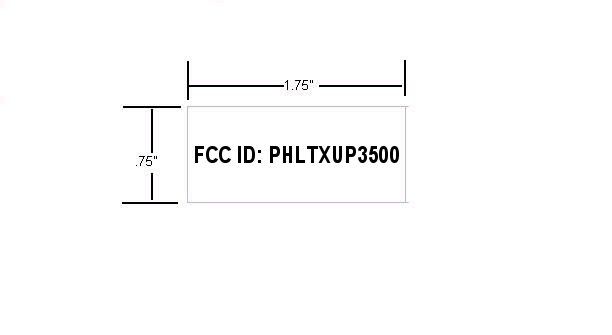
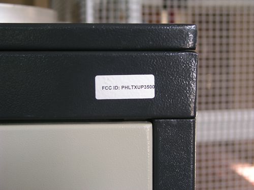
January 26, 2007 Federal Communications Commission Office of Engineering Technology 445 12 th Street SW Washington, DC 20554 Dear Sir, This letter will serve to address FCC correspondence letter 32366 and 32424 regarding the type certification for the Elettronika TXUP3500 broadcast transmitter. The associated FCC ID number is PHLTXUP3500. Specifically, the correspondence letter identified above seeks additional information on how the transmitter is configured regarding whether integral components are the same for both frequency ranges of the proposed grant frequencies. As the technical consultant for Elettronika, they have authorized me to provide information which should help resolve this question. It is my technical opinion that only one set of test data needs to be submitted for both frequency ranges 470-608 MHz and 614-806 MHz based upon the design of the unit. The design of the unit is such that the transmitter works over the entire 470-806 MHz with no change of parts. The only frequency dependent parts within the transmitter are the channel filter in the exciter and transmitter final bandpass filter. The exciter filter is a passive device and consists of one item that is tuned per operating channel. Likewise the transmitter final bandpass filter is a passive device and is the same block of material but it is tuned to the desired operating channel. The performance obtained at any test frequency within the entire range of 470-806 MHz will be representative of each transmitter shipped. If there are any clarifications needed or you have any questions please give me a call at the number above. Sincerely, Greg Best President Cc Maria Quintero, Elettronika America Greg Best Consulting, Inc. 9223 N. Manning Ave. Kansas City, MO 64157 816-792-2913
External Photos
TXUP3500 EXTERNAL CONSTRUCTION PHOTOS FRONT VIEW TOP FRONT VIEW BOTTOM FRONT VIEW REAR VIEW LEFT SIDE RIGHT SIDE
Internal Photos
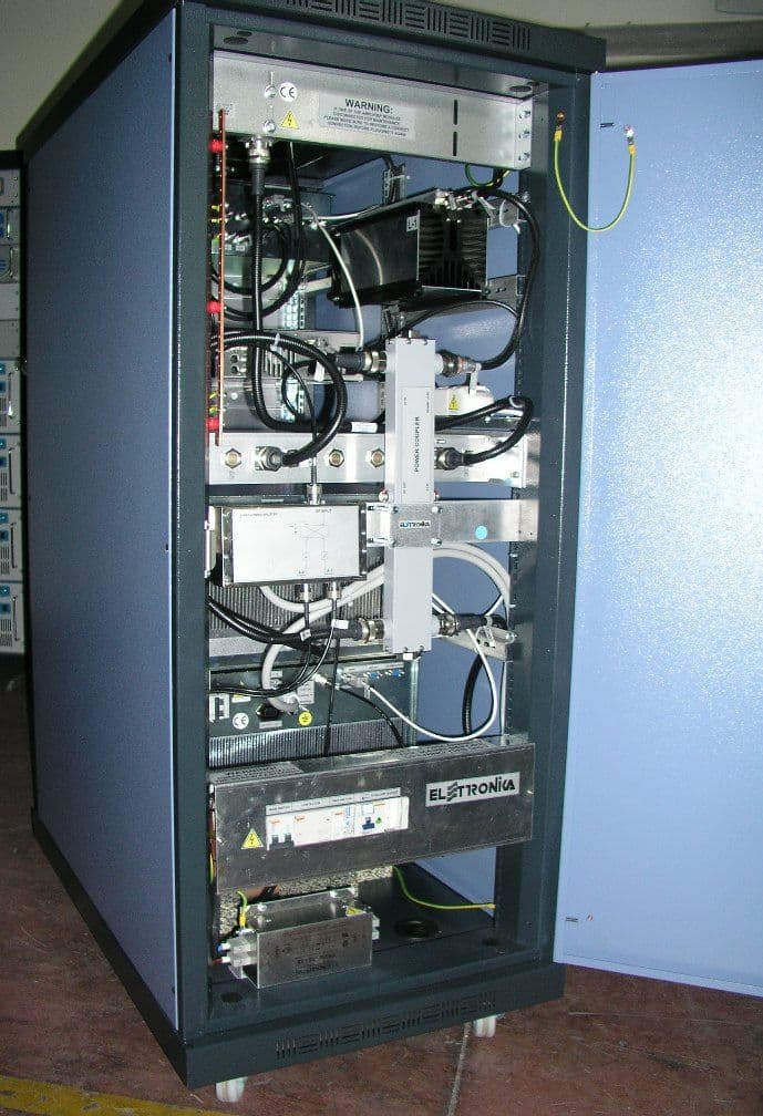
TXUP3500 INTERNAL CONSTRUCTION PHOTOS TOP REAR VIEW-DOOR OPEN BOTTOM REAR VIEW—DOOR OPEN RIGHT SIDE WITHOUT SIDE PANEL LEFT SIDE WITHOUT SIDE PANEL INSIDE ANGLED VIEW
Operational Description
AUTV/3500LD LDMOS - UHF TV SOLID STATE AMPLIFIER INTRODUCTION The AUTV/3500LD belongs to the High Power UHF products family of Television Transmitters fully in solid state technology. The AUTV/3500LD series represents the 3.5kW TV Transmitters operating in the IV/V Band for Common amplification process (separate amplification available) of the Vision and Sound carriers. This Transmitters family has been designed to offer to the customer high performances, high reliability and greater simplicity in their operation and maintenance procedures. The Vision and Sound signal processing is provided for all TV Standards and all types of Audio applications (Mono & Dual sound - NICAM) together with colour systems such as PAL - NTSC - SECAM. Thanks to the amplitude and phase pre- correction circuit, it is possible to cancel the distortions in the output stage, thus cutting down the operating costs. The RF transposition in the driver is carried out by a synthesizer with various possibilities of accuracy and stability as well as precision offset locked by internal or external frequency reference. The RF amplifier is made up by three RF modules installed in a power rack, the modules are dedicated for the Vision and Sound carriers common amplification. The amplifiers employ solid state LDMOS technology in order to obtain wide band, reliability, and high efficiency. Each RF module has a built-in switching- mode power supply unit, self-protected against overcurrents and overvoltages, as well as overtemperature and VSWR for RF parameters. The cooling system is fully contained into the transmitter. The control unit provides full management of the transmitter without the presence of the operator, the system includes a central controller and several peripheral units installed in each RF module and rack. The control device includes a fault finding system to detect equipment malfunctions and locate the faulty subassembly which needs to be replaced. The interlock circuit is independent on the software and remains always operational whether computer control is present or not. The operator interface is made by a high resolution LCD graphic display and a simple keyboard, the menu is very friendly and easy to use. The Control Unit can be fully controlled in REMOTE mode via link or via modem in RS232 or other interface. The equipment design allows the soft degradation (RF power loss) for several transistors faults.
Parts List/Tune Up Info
29 Part Name CodeDescriptionQty CON0145CON0145R0 POST. CASS. CONTROLLO APG012B1 05504CON0134R0 PIANO PROF. 260 ARE. p. 02047 ZN1 05525LAT. 3U PROF. 260 TAV. 424/A p. 2033 ZN2 PAN0066PAN0066R0 PANNELLO CONTR. APG012B 3U1 CON0153CON0153AR0 BASE CASS. CONTR. x APG012 ZN1 0552BKIT MANIGLIE 3-4U cod. 235.0122 02880SPINA V.DE 10A + INT. + FUS. DA PANN. BZ15011 1 SCH0239AR0SCHEDA DI CONTROLLO CON DISPLAY1 SCH0110BR0SCHEDA 3 IN. ANALOGICI MASTER APG012B1 SCH0152AR0SCHEDA COMMUTAZIONE 220VAC x APG012B1 SCH0241AR0SCHEDA IN/OUT DIGITAL SIGNAL FOR APG012C 1 E0031ALIM. SWITCHING S-60-241 07926PROTEZIONE IN GOMMA PVC PG 0871 02843SPINA SCHERM. 2 POLI cod. 525.25521 02695CONNETTORE DB9F x CAVO IU0080591 02856CONNETTORE DB25F x CAVO 525-28121 07925PROTEZIONE IN GOMMA PVC PG0751 07524AINTERR. NERI I39101 02018GE 35145D/22 BN(UG909/cxRG174)1 02035PRESA BNC/F x RG316 cod. 601401 08500CAVO RG174 50W0,30 02700CONNETTORE cod. 534-2303 FEM. 16 VIE1 02790CONNETTORE DB25M x CAVO SALDATO 525-2602 1 02871ACALOTTE PER DB25 cod. 525-26221 C0814NASTRO CONDUT. IN RAME DA 25mm 264/92750,50 V0761TAPPI NERI O 12.7 PLASTICA DP-5005 Component listAPG012C - Amplifier Control 37 COMPONENT LIST SCH0239AR0 Part Name/NumberDescriptionQty. Comps. Page 1/2 BATT BH001RB 3093_9003093 03090 BATTERY HOLDER1BATT1 BZ AI-155 0370503705 5VDC BUZZER1BZ1 CC 100nF-S 01065C01065C Y5V 1206 COND33C10, C15, C17-19, C22, C25, C28, C38, C45, C49-52, C55, C62-63, C68-69, C78, C80-85, C87-88, C90, C92-95 CC 15pF-S 0108801088 SMD 1206 COND2C74-75 CC 1nF-S 0109601096 SMD 1206 COND20C12-14, C31-33, C42-43, C53-54, C56-58, C60-61, C66, C76-77, C79, C86 CC 1uF100V-S 01760A01760A Y5V 1206 COND <<50 V>>8C21, C23, C37, C64-65, C67, C71-72 CC 220pF-S 0109301093 SMD 1206 COND8C2-9 CC 47pF-S 0110001100 SMD 1206 COND8C20, C30, C35-36, C40-41, C48, C59 CE 10uF16V-S01626B TANT. ELETTR SMD CO8C24, C26-27, C29, C34, C39, C46-47 CE 1uF50V-S 01763A01763A ELETTR SMD COND2C89, C91 CE 220uF50V LOW ESR1799A ELETTR SMD COND LOW ESR 4C16, C44, C70, C73 CE 47uF35V-S 01790A01790A ELETTR SMD COND1C11 CE 47uF50V-S 01791C01791C ELETTR SMD COND1C1 D 1N4148-S 0300203002 SMD DIODE4D12-13, D17, D19 D 50WQ06FN03019A SMD DIODE SCHOTTKY 5,5A 1D9 D BAS85-S03024 SMD DIODE SCHOTTKY8D1-8 D BAT54S03199 SMD SCHOTTKY DIODE A-K T 6D10-11, D14-16, D18 DIS WG240128B03083 240/128 DOT MATRIX LCD1LCD1 DL KA-3528SGC 0305703057 GREEN SMD LED DIODE1DL1 DL LEDG3 0305303053 GREEN LED DIODE 3mm1DL3 DL LEDR3 0305803058 RED LED DIODE 3mm4DL2, DL4, DL6-7 DL LEDY3 0305103051 YELLOW LED DIODE 3mm1DL5 IC 24LC64 0481504815 SMD INTEG CIRCUIT1IC7 IC 74HC00-S 4762A4762A SMD INTEG CIRCUIT1IC19 IC 82B715-S 04734A04734A SMD INTEG CIRCUIT1IC17 IC CD4053BC-S 04710A04710A SMD INTEG CIRCUIT1IC12 IC LM2596S-5.004580 SMD INTEG CIRCUIT1IC14 IC LM75-S 0066800668 SMD INTEG CIRCUIT1IC8 IC LMC6482-S04632 SMD INTEG CIRCUIT1IC20 IC LMC6484-S04634 SMD INTEG CIRCUIT4IC2-5 IC M41T56 0461104611 SMD INTEG CIRCUIT1IC6 IC MAX232-S 04804B04804B SMD INTEG CIRCUIT1IC16 IC MAX3080-S 0477004770 SMD INTEG CIRCUIT1IC22 IC MAX3080-S N.M.NOT MOUTED SMD INTEG CIRCUIT 1IC18 IC MAX942CSA-S04572 SMD INTEG CIRCUIT4IC9-11, IC13 IC MB90F543PF04596 SMD INTEG CIRCUIT1IC15 IC MPC100T-450I-TT04577 SMD INTEG CIRCUIT1IC21 IC ULN2003A 487004870 SMD INTEG CIRCUIT2IC1, IC23 IND MS85 10uH-S04948 INDUCTOR 2,7A1L1 IND T100uH-1.8A 495804958 TOROIDAL-STORAGE CHOKES 1L2 38 Part Name/NumberDescriptionQty. Comps. Page 2/2 INV IN-D43A-5V03085 DC/AC MODULE1INV1 J DB9_F-0∞ LT02794 PCB CONNECTOR DB9 LONG T 1J6 J FC-10P 02697-0269902697+02699 PCB CONNECTOR POL 2J11, J13 J FC-16P 02701-0270002701+02700 PCB CONNECTOR POL 2J12, J14 J FC-26P 02855-0285402855+02854 PCB CONNECTOR POL 1J10 J PAN2 0273902739 PCB CONNECTOR1J4 J PAN2 02739-40-4102739+02740+02741 PCB CONNECTO 1J5 J PAN3 0270702707 PCB CONNECTOR3J1-3 J PAN3 NOT MOUNTEDNOT MOUNTED PCB CONNECTOR 2J8-9 J SCREWCONN2 0285302853 PCB SCREW CONNECTOR1J7 JU JUMP3 02707-0274202707+02742 MASCHIO PAN34JP1-4 R 100R-S 00029A00029A RES 1/4W 5% SMD 12066R109, R114, R119-121, R123 R 10K-S 00053A00053A RES 1/4W 5% SMD 120637R22-27, R30, R32-33, R40, R47, R50, R57, R68, R81-82, R85, R90-101, R105-108, R116, R118, R122, R124 R 120R-S 00030A00030A RES 1/4W 5% SMD 12062R112-113 R 1K0-S 00041A00041A RES 1/4W 5% SMD 12065R46, R54, R87-88, R104 R 1K5-S 00043A00043A RES 1/4W 5% SMD 12062R110-111 R 22K-S 00057A00057A RES 1/4W 5% SMD 120611R18, R20-21, R28, R34, R36, R38-39, R41, R43-44 R 2K2-S 00045A00045A RES 1/4W 5% SMD 12068R19, R35, R37, R42, R45, R53, R59-60 R 330R-S 00035B00035B RES 1/4W 5% SMD 12062R89, R103 R 33R-S 00023A00023A RES 1/4W 5% SMD 12062R86, R102 R 470K-S 00073A00073A RES 1/4W 5% SMD 12068R48-49, R51-52, R55-56, R58, R65 R 470R-S 00037A00037A RES 1/4W 5% SMD 120630R10-17, R29, R31, R61-64, R66-67, R69-80, R83-84 R 4K7-S 00049A00049A RES 1/4W 5% SMD 12061R117 R 820R-S 00040A00040A RES 1/4W 5% SMD 12061R9 RL 30.22.24 0756907569 RELE5RLY1-5 RV 10K-S-H 0071500715 VARIABLE RESISTOR1R115 RV 1M-3266X00815 VARIABLE RESISTOR8R1-8 SW SWITCH-4DIP 90∞07531A PCB DIP SWITCH 90∞1SW1 SW SWITCH-8DIP07530A PCB DIP SWITCH SMD1SW2 T 06086 N 7630 76327630 7632 KTI06086 PULSANTE 24T1-4 TR BC848 0345703457 NPN SMD TRANSISTOR1TR1 XTAL 32.768k-S 0514605146 QUARTZ1XTAL1 XTAL 4MHz-S 05101A05101A QUARTZ1XTAL2 41 220VAC SWITCHING BOARDSCH0152AR0 Component layout SCH0152AR0 COMPONENT LIST SCH0152AR0 Part Name/NumberDescriptionQty. Comps. CC 2nF2 2kV 01045A01045A CERAMIC COND3C1-3 D 1N4148 0300103001 DIODE6D1-6 FUSE OMEGA C1034FUS00008 PORTA FUSIBILE 5x20 D1F1 J CON HD515V/05-6PVE02883 + 02884 PANDUIT PCB CONN1J1 J FC-10P 02697-0269902697+02699 PCB CONNECTOR POL1J9 J VASCHETTA IEC02879 VASCHETTA FEMALE PCB3J6-8 JU JUMP2 02739-0274202739+02742 MASCHIO PAN21JP1 RL 40.31.247567C RELE3RLY1-3 43 IN/OUT DIGITAL BOARDSCH0241AR0 Component layout SCH0241AR0 COMPONENT LIST SCH0241AR0 Part Name/NumberDescriptionQty. Comps. DZ 5V1 0310903109 ZENER DIODE1DZ1 FUSE OMEGA C1034FUS00008 PORTA FUSIBILE 5x20 D1F1 J BNC-90G-PCB 203402034 PCB CONNECTOR2J2-3 J DB9-90G 0279702…
Text truncated - open the document above for the full version.
Schematics
28 32 33 34 35 36 40 42 44 47 0.47U/50V 471/1KV 471/1KV 222/500V 15V24V 104/100V104/100V 30V12V 0.47U/50V 472/100V 1U/50V 5V S-60N DIFFERENT COMPONENT: C18 103/50V C20 103/50V C13 R13 1K C31 203/100V 3022 U3 R12 5K1 C14 223/50V 2 7 6 18 5 4 3 3842 U1 R10 680 R11 7K5 R7 5K1 R14 R9 C16 221/1KV C15 471/50V 2200U/10V C22 C21 2200U/10V 2200U/10V 2200U/10V C23 C24 C25 2200U/10V 330U/35V X 330U/35V X 470U/25V 470u/25V 1000U/25V 1000U/25V X 1000U/25V 470U/25V X 330U/35V470U/25V X 470u/25V 330U/35V 330U/35V 330U/35V X U2 PC111 C12 474/250VAC C1 C28 221/250VAC C32 221/250VAC FG AC/NFG RTH1 10SP005 ZNR1 471 F 3A/250V FS1 AC/L BD1 4A/800V R1 680K/1/2W TF-096C1 LF1 472/250VAC C3 C2 472/250VAC C6 222/250VAC 104/250VAC C4 R8 22 103/50V C11 3 C9 47u/50V Q1 2SK727 1 R5 5.1 D2 FR104 R29 47K/2W 5 T1 C5 150u/400V R4 47K/2W V- R3 30K/3W R2 330/3W 473/400V C7 7 D1 EGP20J 101/1KV C8 D4D4 14-16 C20 R27 L2 C21 10-13 C22 C23 C24 R23 ZD3 JUMP R17 U2 PC111 R22 2K2 BYQ28X-200 RB009RB009RB009 BYQ28X-200BYQ28X-200BYQ28X-200 RB009 15K15K 12K 7K5 15K 20K 1K5 24K 22K R17 R14 10K D4 L2 RB016 CTB34M 2K C10 472/50V R6 2 1K5 R18 R19 R18 C18 R21 470 SHR1 TL431 SVR1 1K 100 22 R20 R23 R26 R27 560 5.1/1/2W 2K 100 390 2K 390 100 2K 22 220 220 22 5.1/1/2W5.1/1/2W 2K74K72K7 47/1/2W 10K 47/1/2W 820 0.39/2W 1K/2W 820820 0.39/2W0.39/2W 680/2W270/2W 0.39/2W 270/2W 820 TF159-1 13.8V TF161-1 TF160-1TF158-1 17.9V26.9V 33V/1W TF161-1 T1 R6 0.33/2W 39/2W R28 680 R9 5.1V ZD2 U3 3022 R20 C12 R19 103/50V 3K3 222/50V 10K 222/50V222/50V 20K10K 222/50V 2…
Text truncated - open the document above for the full version.
Contact Information
Applicant
Francesco Paparella(Design Omologation and Compliance Mgr)
Technical Contact
Greg Best Consulting Inc.Greg Best
[email protected]816-792-2913
9223 N. Manning Avenue · Kansas City, Missouri · United States
Technical Specifications
| # | Rule Parts | Frequency Range | Power Output | Emission | Tolerance |
|---|---|---|---|---|---|
| 2 | 73,74 | 614 MHz - 806 MHz | 350 W | 250KF3E | 1000 Hz |
Other Applications from Elettronika S.r.l.
PHLTXUD1000A
Jul 07, 20101000 W ATSC Transmitter
Equipment Class
TBC - Licensed Broadcast Station Transmitter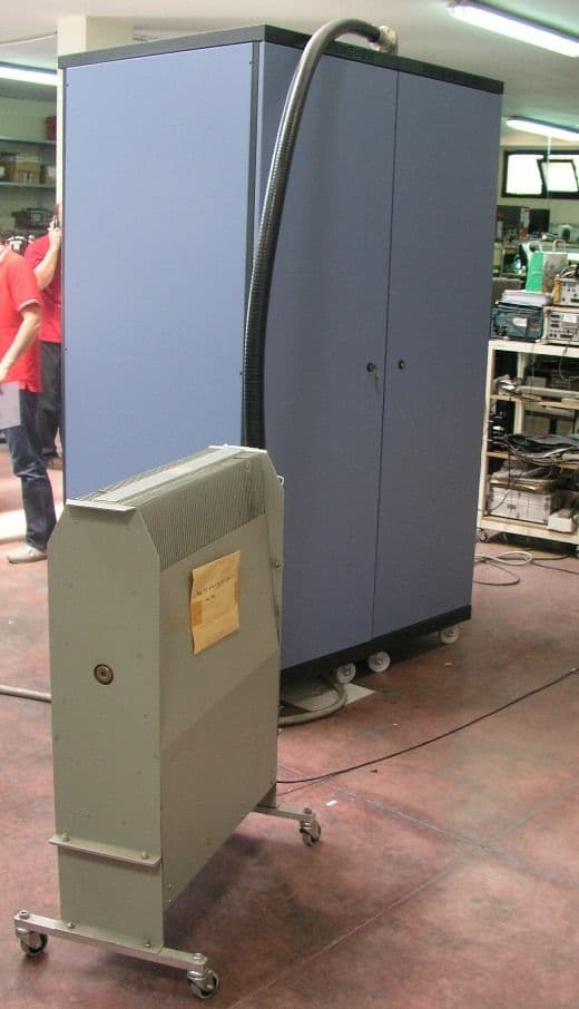
PHLTXUD3000A
Jun 17, 20103000 Watt ATSC Transmitter
Equipment Class
TBC - Licensed Broadcast Station Transmitter
PHLTXUD2000A
Jun 09, 20102000 Watt ATSC Transmitter
Equipment Class
TBC - Licensed Broadcast Station Transmitter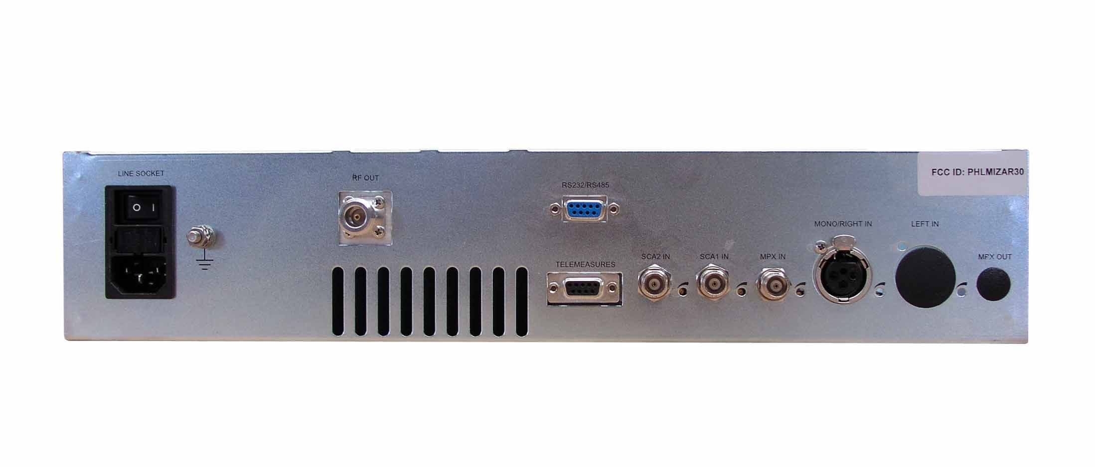
PHLMIZAR30
Jul 01, 200830 Watt FM Broadcast Transmitter
Equipment Class
TBC - Licensed Broadcast Station Transmitter
PHLMIZAR300
Jul 01, 2008300 Watt FM Broadcast Transmitter
Equipment Class
TBC - Licensed Broadcast Station Transmitter