PJ7-112XGPRS Module
Shenzhen Neoway Technology Co., Ltd.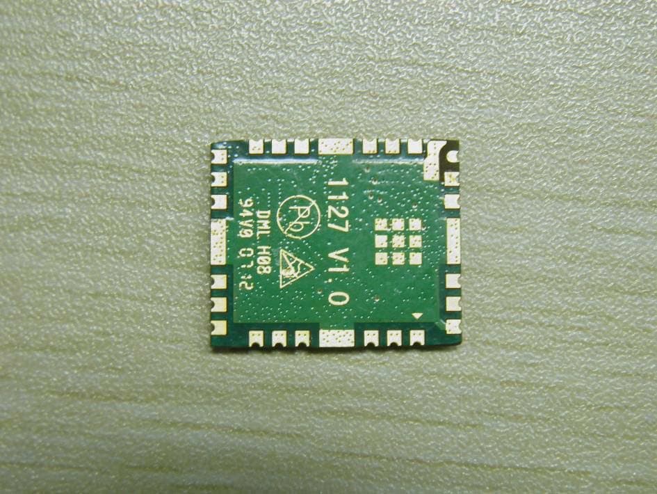
Click to zoom
Application Details
- Equipment Class
- PCB - PCS Licensed Transmitter
- Date of Grant
- Sep 05, 2012
- Application Purpose
- Original Equipment
- Date of Application
- Sep 05, 2012
- Equipment Note
- GPRS Module
- Frequency Range
- 1850.20000000 - 1909.80000000
- Country
- China
Documents & Files
Document Text
Text extracted from the exhibit documents filed with the FCC. Open a document above to read the original.
Users Manual
Neo_M660 User Manual V ersion V1.0 Shenzhen Neoway Technology Co.,Ltd Neo_M6 60 User Manual V1.0 All rights reserved by Shenzhen Neoway Technology Co., Ltd Page 2 Total 11 Cop yright Statement Cop yright © 2008 Neoway Technology All rights reserved by Shenzhen Neoway Technology Co.,Ltd. The trademark belongs to Shenzhen N eoway Technology Co.,Ltd. Other trademarks in this manual belongs to their owners. Clarification This specification is for system engineer, research engineer and test engineer. As the upgrading of the product version or some other reasons, we’ll do some necessity updating to the content of this specification without advance notice. Unless we have other additional assumpsit, all statements, information and suggestions in this manual do not constitute any express or implied guarantees. Shenzhen Neoway Technology Co.,Ltd can supply all the technological support. If you have any problem, please feel free to contact to the sales representative or send E-mail to these two mailboxes: [email protected] [email protected] W ebsite: www.neoway.com.cn All rights reserved by Shenzhen Neoway Technology Co., Ltd Page 2 Total 12 Neo_M6 60 User Manual V1.0 All rights reserved by Shenzhen Neoway Technology Co., Ltd Page 3 Total 11 Content s 1 Overview 2 Figuration 3 Block Diagram 4 Character 5 Pin Definition & Encapsulation 5.1 Pin Definition ...........................................................................8 5.2 PCB Packaging .......................................................................9 6 General AT Commends 7 Call Control Commends 8 TCP/UDP AT Commends 9 Assembling All rights reserved by Shenzhen Neoway Technology Co., Ltd Page 3 Total 12 Neo_M6 60 User Manual V1.0 All rights reserved by Shenzhen Neoway Technology Co., Ltd Page 4 Total 11 Revisio n Record Version Content Revised Effective date V1.0 Initial version 2012-06 All rights reserved by Shenzhen Neoway Technology Co., Ltd Page 4 Total 12 Neo_M6 60 User Manual V1.0 All rights reserved by Shenzhen Neoway Technology Co., Ltd Page 5 Total 11 1 Overview M660 is an open platform that supports GSM/GPRS wireless industry module, reserved CPU resources and a wealth of hardware interface which is widely used in various industrial and commercial fields to provide high quality voice, message, data business and other functions. 2 Figuration T able 2-1 M660 Figuration Specification Specifica tions Des cription Dimen sions 23. 6mm*23.6mm*2.6mm ( length* width*height) Weig ht 2.8 g Overview 3 Block Diagram Baseband Controller PA Power Manager Application Interface RF Section FLASH Audio Section SIM UA RT All rights reserved by Shenzhen Neoway Technology Co., Ltd Page 5 Total 12 Neo_M6 60 User Manual V1.0 All rights reserved by Shenzhen Neoway Technology Co., Ltd Page 6 Total 11 4 Character T able 4-1 General p arameters Description Operatin g temperature -30+70 Operatin g voltage 3.5V4.3Vrecommendation 3.9V Operatin g Current See table 4-2 and 4-3 S torage temperature -40+80 Humidity ran ge 0%95% T able 4-2 GSM S pecifications Description Freque ncy 900/1800/850/1900 Sensitivity -106dBm 850/90 0 Class4(2W) The Maximum transmi ssion Power 1800/1 900 Class1(1W) Protocol Compatible with GSM/GPRS Phase2/2+ GSM07.07 AT Extended co mmand sets Audio FREFRHRAMR voice coding TEXT/PDU SMS Point to point/cell broad cast Grou ped Data GPRS CLASS 12 Codin g scheme CS1~CS4 Mobile Station type Class B Suppo rt CSD data service Circuit Switch ed Data Suppo rt USSD Call forwardCFB,CFNA,CFU Call waiting Supp lement Service Three way calling Main Processor ARM7-EJ@104MHz, 32Mbits SRAM,32~64Mbits Nor Flash R eserved software 16Mbits RAM16~32Mbits Flash All rights reserved by Shenzhen Neoway Technology Co., Ltd Page 6 Total 12 Neo_M6 60 User Manual V1.0 All rights reserved by Shenzhen Neoway Technology Co., Ltd Page 7 Total 11 resource R eserved software resource UART x 2I2CLCDSPIMMCUSBADCPWM GPIO x 20Keypad Inst antaneous Current Max 1.8A A verage working Current 300mA S tandby Current 2.5mA typ. All rights reserved by Shenzhen Neoway Technology Co., Ltd Page 7 Total 12 Neo_M6 60 User Manual V1.0 All rights reserved by Shenzhen Neoway Technology Co., Ltd Page 8 Total 11 5 Pin Definition & Encapsulation 5.1 Pin Definition The signal connection uses 28pin SMD p ad of stamp hole(half hole). Note: M660 module IO interface level is 2.8V. Because the module IO uses 2.8V power supply system, the maximum input voltage of all the IO interface can not exceed the maximum 3.3V, otherwise it may damage the module IO. Considering the signal integrality designing reasons,while the external circuit use 3.3V power system the IO interface output voltage will exceed 3.3V because of overshoot phenomenon, sometimes can even reach 3.5V.Therefore,the IO pin of the module will be damaged if 3.3V IO signal is connected to 2.8V IO of the module directly. Table 5-1 M660 Pin Definition Pin Signal Name I/O Function De scription Rem ark 1 VSIM PWR Main Power Compatible to 1.8/3.0V SIM card 2 SIM_CLK DO Clock of SIM card 3 SIM_DATA DIO Data input & output of SIM card Built-in 5K pull-up resistor 4 GND PWR GRAND 5 SIM_RST DO SIM card reset 6 MICP AI Positive electrode of MIC audio input Alternating peak voltage≤200mV 7 MICN AI Negative electrode of MIC audio input Alternating peak voltage≤200mV 8 EARP AO Positive electrode of 32Ω earphone driving output All rights reserved by Shenzhen Neoway Technology Co., Ltd Page 8 Total 12 Neo_M6 60 User Manual V1.0 All rights reserved by Shenzhen Neoway Technology Co., Ltd Page 9 Total 11 earp hone audio output 9 EARN AO Negative electrode of earphone audio output 32Ω earphone driving output 10 DTR DO Low power consumption set 11 GND PWR Grand 12 RING DI Ring output 13 VCCIO PWR 2.8V output Can be supplied to IO level shift circuit, loading capacity < 50mA 14 Reserved Reserved 15 Reserved Reserved 16 URXD DI UART data receiving 17 UTXD DO UART data transmitting Used to GPRS communications and AT commands 18 GND PWR Grand 19 Res et…
Text truncated - open the document above for the full version.
ID Label/Location Info
EXHIBIT A - FCC ID LABELING AND LOCATION FCC ID Labeling FCC ID Location Label here The label shown shall be permanently affixed at a conspicuous location on the device and be readily visible to the user at the time purchase (Labeling requirements per 2.925)
Internal Photos
EXHIBIT C - EUT INTERNAL PHOTOGRAPHS EUT – Shielding off View EUT – Main Board Top View EUT – Main Board Bottom View
RF Exposure Info
Bay Area Compliance Laboratories Corp. (Shenzhen) Report No.: RSZ120816006-00 FCC Part 22H/24E Page 9 of 30 FCC §1.1307 (b) (1) & §2.1091 - MAXIMUM PERMISSIBLE EXPOSURE (MPE) Applicable Standard According to subpart 1.1307 (b)(1), 2.1091systems operating under the provisions of this section shall be operated in a manner that ensures that the public is not exposed to radio frequency energy level in excess of the Commission’s guidelines. Limits for Maximum Permissible Exposure (MPE) (§1.1310, §2.1091) (B) Limits for General Population/Uncontrolled Exposure Frequency Range (MHz) Electric Field Strength (V/m) Magnetic Field Strength (A/m) Power Density (mW/cm 2 ) Averaging Time (minutes) 0.3–1.34 614 1.63 *(100) 30 1.34–30 824/f 2.19/f *(180/f²) 30 30–300 27.5 0.073 0.2 30 300–1500 / / f/1500 30 1500–100,000 / / 1.0 30 f = frequency in MHz; * = Plane-wave equivalent power density; According to §1.1310 and §2.1091 RF exposure is calculated. RF Exposure Evaluations Predication of MPE limit at a given distance S = PG/4πR² Where S= power density (in appropriate units, e.g. mW/cm 2 ) P = power input to the antenna (in appropriate units, e.g., mW) G = Antenna Gain in linear scale R = distance to the center of radiation of the antenna (appropriate units, e.g., cm) Maximum Permissible Exposure (MPE) Calculations Frequency (MHz) Max Ant. Gain (dBi) Max Conducted Output Power (dBm) Duty Cycle Evaluation Distance (cm) Power Density (mW/cm 2 ) MPE Limit (mW/cm 2 ) Results 824 7 33 25% 20 0.498 0.549 Pass 1850 3 30 25% 20 0.099 1.0 Pass Note: FCC Part 22H Limit = 7 Watts = 38.45 dBm (ERP), Part 24E Limit =2 Watts = 33 dBm (EIRP) Conclusion: Based on FCC §1.1310 and §1.1091, the EUT will comply with FCC rules on RF exposure for mobile devices if the antenna gain does not exceed 7 dBi in cellular band and 3 dBi in PCS band. An appropriate RF exposure compliance statement will be placed in the user’s guide.
Test Report
Note: This test report is prepared for the customer shown above and for the device described herein. It may not be duplicated or used in part without prior written consent from Bay Area Compliance Laboratories Corp. This report must not be used by the customer to claim product certification, approval, or endorsement by NVLAP*, or any agency of the Federal Government. * This report may contain data that are not covered by the NVLAP accreditation and shall be marked with an asterisk “★” FCC PART 22H, PART 24E MEASUREMENT AND TEST REPORT For Shenzhen Neoway Technology Co., Ltd. 4F-2#, Lianjian Science & Industry Park, Huarong Road, Dalang, Longhua, Bao’an District, Shenzhen, Guangdong, China FCC ID: PJ7-112X Report Type: Original Report Product Type: GPRS Module Test Engineer: Brown Lu Report Number: RSZ120816006-00 Report Date: 2012-08-24 Reviewed By: Sula Huang EMC Engineer Test Laboratory: Bay Area Compliance Laboratories Corp. (Shenzhen) 6/F, the 3rd Phase of WanLi Industrial Building ShiHua Road, FuTian Free Trade Zone Shenzhen, Guangdong, China Tel: +86-755-33320018 Fax: +86-755-33320008 www.baclcorp.com.cn Bay Area Compliance Laboratories Corp. (Shenzhen) Report No.: RSZ120816006-00 FCC Part 22H/24E Page 2 of 30 TABLE OF CONTENTS GENERAL INFORMATION.......................................................................................................................................4 PRODUCT DESCRIPTION FOR EQUIPMENT UNDER TEST (EUT) .....................................................................................4 OBJECTIVE...................................................................................................................................................................4 RELATED SUBMITTAL(S)/GRANT(S).............................................................................................................................4 TEST METHODOLOGY..................................................................................................................................................4 TEST FACILITY.............................................................................................................................................................5 SYSTEM TEST CONFIGURATION ..........................................................................................................................6 JUSTIFICATION.............................................................................................................................................................6 EQUIPMENT MODIFICATIONS.......................................................................................................................................6 SUPPORT EQUIPMENT LIST AND DETAILS....................................................................................................................6 EXTERNAL I/O CABLE..................................................................................................................................................6 BLOCK DIAGRAM OF TEST SETUP................................................................................................................................7 SUMMARY OF TEST RESULTS ...............................................................................................................................8 FCC §1.1307 (B) (1) & §2.1091 - MAXIMUM PERMISSIBLE EXPOSURE (MPE)..................................................9 APPLICABLE STANDARD..............................................................................................................................................9 RF EXPOSURE EVALUATIONS......................................................................................................................................9 FCC §2.1047 - MODULATION CHARACTERISTIC ............................................................................................10 FCC §2.1046, §22.913 (A) & §24.232 (C) - RF OUTPUT POWER.........................................................................11 APPLICABLE STANDARD............................................................................................................................................11 TEST PROCEDURE......................................................................................................................................................11 TEST EQUIPMENT LIST AND DETAILS.........................................................................................................................11 TEST DATA................................................................................................................................................................12 FCC §2.1049, §22.917, §22.905 & §24.238 - OCCUPIED BANDWIDTH ..............................................................14 APPLICABLE STANDARD............................................................................................................................................14 TEST PROCEDURE......................................................................................................................................................14 TEST EQUIPMENT LIST AND DETAILS.........................................................................................................................14 TEST DATA................................................................................................................................................................14 FCC §2.1051, §22.917(A) & §24.238(A) - SPURIOUS EMISSIONS AT ANTENNA TERMINALS ..................18 APPLICABLE STANDARD............................................................................................................................................18 TEST PROCEDURE......................................................................................................................................................18 TEST EQUIPMENT LIST AND DETAILS.......................................................................…
Text truncated - open the document above for the full version.
Test Setup Photos
EXHIBIT D - TEST SETUP PHOTOGRAPHS Radiated Emission Test View Frequency Stability Test View
Contact Information
Applicant
Jesse Yuan(Certification Manager)
Test Firm
Bay Area Compliance Laboratory Corp. (Shenzhen)John Chan
Technical Specifications
| # | Rule Parts | Frequency Range | Power Output | Emission | Tolerance |
|---|---|---|---|---|---|
| 2 | 24E | 1.85 GHz - 1.91 GHz | 906.00 mW | 312KGXW | 2.5 ppm |
Other Applications from Shenzhen Neoway Technology Co., Ltd.
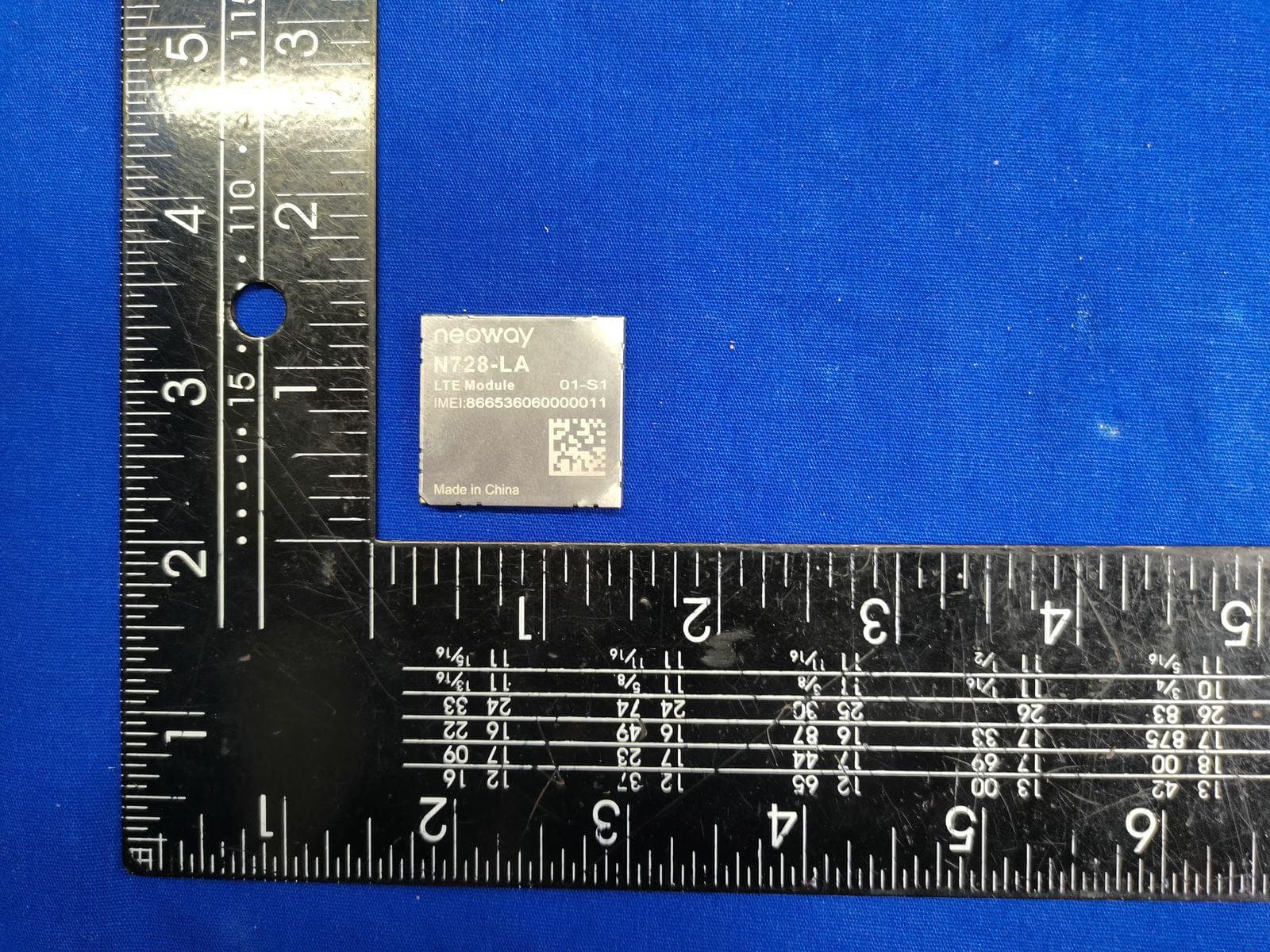
PJ7-N728LA
Aug 05, 2023LTE Module
Equipment Class
PCB - PCS Licensed TransmitterPJ7-N2110-AM
Jul 13, 2020LTE OBD dongle
Equipment Class
JAB - Part 15 Class B Digital Device
PJ7-N2610-US
Jul 09, 2020LTE OBD dongle
Equipment Class
JAB - Part 15 Class B Digital Device
PJ7-N27-W3
Apr 28, 2020Cat.M1 Module
Equipment Class
PCB - PCS Licensed Transmitter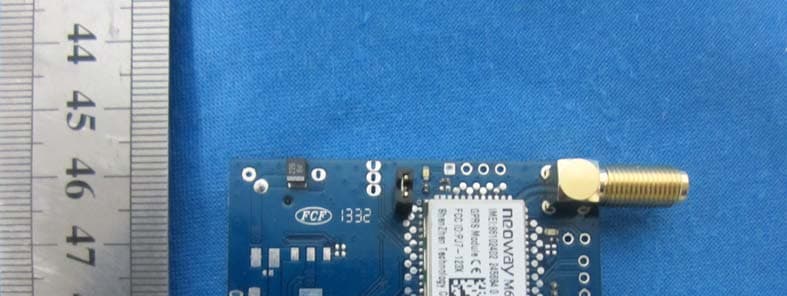
PJ7-1232
Mar 19, 2014GPRS Module
Equipment Class
PCB - PCS Licensed Transmitter