PL4F701LSA1010021MP701 LCD Monitor
CORNEA TECHNOLOGY CO., LTD.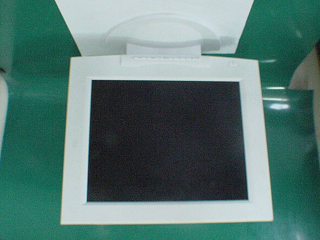
Click to zoom
Application Details
- Equipment Class
- JBP - Part 15 Class B Computing Device Peripheral
- Date of Grant
- Aug 05, 2001
- Application Purpose
- Original Equipment
- Date of Application
- Aug 05, 2001
- Equipment Note
- MP701 LCD Monitor
- Company
- CORNEA TECHNOLOGY CO., LTD.
- Country
- South Korea
Documents & Files
Document Text
Text extracted from the exhibit documents filed with the FCC. Open a document above to read the original.
Users Manual
Information to user : PART 15, PARAGRAPH 15.21 The users manual or instruction manual for an intentional or unintentional radiator shall caution the user changes or modifications not expressly approved by the party responsible for compliance could void the user’s authority to operate the equipment FCC Notice For a Class B digital device or peripheral, the instructions furnished the user include the following or similar statement, placed in a prominent location in the text of the manual : NOTE : This equipment has been tested and found to comply with the limits for a Class B digital device, pursuant to Part 15 of the FCC Rules. These limits are designed to provide reasonable protection against harmful interference in a residential installation. This equipment generates, uses and can radiate radio frequency energy and, if not installed and used in accordance with the instructions, may cause harmful interference to radio communications. However, there is no guarantee that interference will not occur in a particular installation. If this equipment does cause harmful interference to radio or television reception, which can be determined by turning the equipment off and on, the user is encouraged to try to correct the interference by one or more of the following measures: - Reorient or relocate the receiving antenna. - Increase the separation between the equipment and receiver - Connect the equipment into an outlet on a circuit different from that to which the receiver is connected. - Consult the dealer or an experienced radio/TV technician for help.
Cover Letter(s)
CORNEA TECHNOLGOY CO., LTD Subject : Application for FCC Certification Dear Sir, Please find enclosed a application and supporting documentation for the following product under FCC Part 15 Subpart B - Applicant : CORNEA TECHNOLOGY CO., LTD.. - Product Name : LCD Monitor - Model name : MP701(alt. Shining17) The following items are enclosed with this application 1. Block diagram 2. FCC ID label sample 3. FCC ID label location information 4. External Photos 5. Internal Photos 6. Schematics 7. Test report 8. Users Manual 9. Part List 10. Test Setup Photos If your have any question or need additional information, please give me a call 82-31-424-9600 (ext.5) / e-mail address : [email protected] Thanks ! Sincerely, Dated this 23 day of March, 2001
Cover Letter(s)
Dear Ms. Mccann, I could speak with Ms. Park at Tokin EMC Engineering and she kindly informed me below so please refer it. The computer used during the test at their facility has no FCC ID nor Doc itself. Because it is very hard to find the computer as the completed product which complys with the FCC so Tokin EMC collected/bought the parts/components which comply with the FCC and assembled the customised computer by themselves. She also said FCC would accept it if the computer consists of the components/parts which has the FCC ID or Doc. The page number 4 in your last mail's attachment shows most of the parts have them except Speaker and Adaptor. She also said the FCC doesn't require the FCC ID or DoC to these two pats. So Tokin EMC judged this report wolud meet with the FCC. I hope this reply would help and solve the matter. Should you have further inquiries, please let me know. Best regards, **************************************************** Tadao Hirose, Mr. Customer Services UL Japan Co., Ltd. Technical Center, Yokohama Business Park 134 Godo-cho, Hodogaya Ward, Yokohama City Kanagawa Prefecture 240-0005 Japan Phone : +81-45-342-1200 (Dept.) Phone : +81-45-342-1208 (Direct in) Facsimile : +81-45-342-1601 E-mail : [email protected] **************************************************** Lyn A. Mccann 2003/03/29 07:40 To: Tadao Hirose/TKY/ULI@ULI cc: Subject: Re: Assistance from CS in UL Japan Dear Mr. Hirose, Thank you so much for such a quick response, attached are 4 original documents from TOKIN concerning the project in question. #1- The proof of conformity has Tokins test report number which may help them find the project. #2- Description of Device. #3-Test Facility and Summary of results, this also has the report writer and the testing engineers name at the bottom. & #4-Tested System Details, this paper should state the FCC ID number for the computer that was used during the testing process or indicate if it was DOC'ed, this is the information I need to resolve this situation. I listed the information the FCC is requiring at the bottom of the "tested system details" document. TOKIN.tif Please ask that the information requested be sent to me As Soon As Possible. Would it be possible to have current information and contact information from TOKIN to keep on file. Mr. Hirose, Once again thank you so much for your help in this unusual situation, your extra efforts are greatly appreciated !!!!!! It has been a pleasure working with you and experiencing first hand the team work and professionalism of UL's CSP's all around the world Lyn McCann International EMC services Conformity Assessment Specialist Underwriters Laboratories Inc. Dept. 3014A.CAM E-mail: [email protected] Ph.: +1-360-817-5655 www.ul.com Tadao Hirose 03/27/2003 05:41 PM To: Akira Kamada/TKY/ULI@ULI cc: Jeffery A. Yates/CAM/ULI@ULI, Ramon J. Torres/CAM/ULI@ULI, Ly Yamazaki/TKY/ULI@ULI, Kunio Sekino/TKY/ULI@ULI Subject: Re: Assistance from CS in UL Japan Dear all, I have just contacted Mr. Fukuda at Tokin EMC Eng. but unfortunately he is out of office by the business trip today. I heard his fax number so I will send this inquiries and I will let you konw when I hear from him. Please wait at least on Monday morning. Best regards, **************************************************** Tadao Hirose, Mr. Customer Services UL Japan Co., Ltd. Technical Center, Yokohama Business Park 134 Godo-cho, Hodogaya Ward, Yokohama City Kanagawa Prefecture 240-0005 Japan Phone : +81-45-342-1200 (Dept.) Phone : +81-45-342-1208 (Direct in) Facsimile : +81-45-342-1601 E-mail : [email protected] **************************************************** Akira Kamada 2003/03/28 08:49 To: Tadao Hirose/TKY/ULI@ULI cc: Ramon J. Torres/CAM/ULI@ULI, Jeffery A. Yates/CAM/ULI@ULI Subject: Re: Assistance from CS in UL Japan Hirose-san, Please take a necessary action for this. Please ask Mr.Sekino to resolve this issue immediately if needed and inform Jeff-san and Ramon-san of the result accordingly. Thanks and best regards, Akira Kamada Customer Service Manager, UL Japan Co., Ltd. Technical Center, Yokohama Business Park 134 Godo-cho, Hodogaya-ku, Yokohama-shi, Kanagawa, 240-0005, JAPAN tel:+81-45-342-1201(direct) fax:+81-45-342-1615(direct) e-m1il: [email protected] 240-0005134 Jeffery A. Yates 2003/03/28 06:52 To: Akira Kamada/TKY/ULI@ULI cc: Ramon J. Torres/CAM/ULI@ULI Subject: Assistance from CS in UL Japan Good morning, I hope you are having a good day Would you please see if you can help us make contact with the company below. As you can see we have a limited amount of time to deal with this issue so your help is much appreciated. Thanks and best regards Jeff Jeff Yates Customer Services Manager _________________________________ Underwriters Laboratories Inc. 2600 N.W. Lake Road Camas, WA 98607-8542 USA Tel: (360) 817-5516 Mobile: (360) 608-9567 Email: [email protected] Lyn A. Mccann 03/27/2003 01:14 PM To: Ramon J. Torres/CAM/ULI@ULI cc: Subject: FCC info added to letter Dear Akira Kamada, My name is Lyn McCann, with Underwriters Laboratories in Camas Washington (West Coast Division). Our EMC department takes on various projects, one of which is being a Telecommunications Certification Body (TCB). We provide the Federal Communications Commission (FCC) with the necessary documents and information to issue FCC Certification (or grant) to companies who market products in the U.S. If the FCC should need information or have questions concerning an issued grant, UL is contacted. We recently received a request for information from the FCC about a grant issued to a company in Japan who’s device was tested by “Tokin EMC Engineering Co., Ltd”. We have made multiple attempts to contact this company over the past 2 weeks and have been unsuccessful. We are requesting your help in trying to contact this company. The FCC gives UL 30 days to submit the requested information. In the event that the information is not submitted within these guide…
Text truncated - open the document above for the full version.
External Photos
FUNCTION KEY
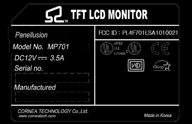
ID Label/Location Info
FCC ID Label Sample CORNEA TECHNOLOGY CO., LTD. LCD Monitor FCC ID : This device complies with PART 15 of the FCC Rules. Operation is subject to the following two conditions : (1) this device may not cause harmful interference, and (2) this device must accept any interference received, including interference that may cause undesired operation.
Internal Photos
Main Board Inside Adapter Inverter LVDS OUTPUT PORT, SPEAKER IN PORT OSD CONNECTION PORT
Internal Photos
MAINBOARD BACK SIDE LVDS OUTPUT PORT MAINBOARD 1 MAINBOARD 2 INVERTER CONNECTION PORT
Operational Description
Operation Description Τηε Μονιτορ ισ χομποσεδ οφ ΛΧ∆ Πανελ Υνιτ, ΤΜ∆Σ Τρανσμιττερ(∆Σ90χ387Α), ΛΧ∆ Χοντρολλερ(ΓΜ5020), ςιδεο Χλοχκ, Μιχροχοντρολλερ χλοχκ(89Χ51), Ινπερτερ ανδ εξτερναλ Ποωερ συππλψ. − Ποωερ Τηε ΑΧ αδαπτερ συππλιεσ ∆Χ12ς το μαιν βοαρδ. Τηε μαιν βοαρδ γενερατεσ ∆Χ3.3ς , ∆Χ5ς ανδ 2.5ς αφτερ τηε ποωερ ον σιγναλ ισ δετεχτδ. Ιτ συππλιεσ ∆Χ5ς, 3.3ς ανδ 2.5ς. − Ινπερτερ Τηε παρτ ινπερτσ ∆Χ το ΑΧ το λιγητ βαχκ λιγητ λαμπ οφ ΛΧ∆ Πανελ Μαιν βοαρδ συππλιεσ σιγναλσ ινπερτερ’σ ον/οφφ ανδ βριγητνεσσ χοντρολ σιγναλ. − ςιδεο Προχεσσινγ(ιμαγε προχεσσ) ΛΧ∆ πανελ ονλψ συππορτσ α ρεσολυτιον (1280 ξ 1024). Τηε σχαλινγ φυνχτιον ισ υσεδ ωηεν τηε ινπυτ ρεσολυτιον ισ λεσσ τηαν τηε πανελ ρεσολυτιον. − Μιχρο Χοντρολλερ Τηε μιχροχοντρολλερ αυτοματιχαλλψ δετεχτσ τηε πιδεο βοαρδ ινσταλλεδ ιν ψουρ σψστεμ. Ωηεν ψου τυρν ον τηε μονιτορ, τηε μιχρο χοντρολλερ φιρστ χηεχκσ τηε δισπλαψ μοδε μεμορψ στορεδ ιν τηε υσερ σεττινγ αρεα ανδ φαχτορψ πρεσεττινγ αρεα. Ανδ τηε χοντρολλερ ηασ ΙΧ ιντερφαχε το χομμυνιχατε ωιτη ΕΕΠΡΟΜ ανδ α διρεχτ βυσ το χομμυνιχατε ωιτη σχαλινγ ΙΧ. Ανδ αν οπερατινγ χλοχκ οφ τηε χοντρολλερ ισ α 20ΜΗζ.
Operational Description
Operation Description The Monitor is composed of LCD Panel Unit, TMDS Transmitter(DS90c387A), LCD Controller(GM5020), Video Clock, Microcontroller clock(89C51), Inverter and external Power supply. - Power The AC adapter supplies DC12V to main board. The main board generates DC3.3V , DC5V and 2.5V after the power on signal is detectd. It supplies DC5V, 3.3V and 2.5V. - Inverter The part inverts DC to AC to light back light lamp of LCD Panel Main board supplies signals inverter’s on/off and brightness control signal. - Video Processing(image process) LCD panel only supports a resolution (1280 x 1024). The scaling function is used when the input resolution is less than the panel resolution. - Micro Controller The microcontroller automatically detects the video board installed in your system. When you turn on the monitor, the micro controller first checks the display mode memory stored in the user setting area and factory presetting area. And the controller has IC interface to communicate with EEPROM and a direct bus to communicate with scaling IC. And an operating clock of the controller is a 20MHz.
Schematics
5 5 4 4 3 3 2 2 1 1 DD CC BB AA 17" LCD MONITOR DESIGN, (ANALOG, DVI, VIDEO, TUNER, AUDIO SUPPORT) SCHEMATIC TOP LEVEL VIDEO DECODER 1 2 3 4 6 7 REVISION HISTORYCONTENTS MCU FRAME STORE MEMORY POWER CONTENTS DateAuthorVerComments CORNEA TECHNOLOGY SignatureApproval CORNEA TECHNOLOGY DateOrganization LVDS OUTPUT PORT 5 Sep 04/00 SHEET YH,LEE OTHER I/O PORT ZOOM SCALER 8 9 10 Initial Release INPUT PORT YH,LEE1.0 AUDIO11 Oct 17/00HK,OH1.1Reference Name Change Nov 29/00YH,LEE1.2Parts Change for Debugging Dec 18/00YH,LEE1.3Change Audio Processor Dec 27/00HK.OH1.4Reference Name Change CONTENTS A 111Thursday, December 28, 2000 1.4 MS701-M Title SizeDocument NumberRev Date:Sheetof 5 5 4 4 3 3 2 2 1 1 DD CC BB AA CORNEA TECHNOLOGY MS701-M1.4 TOP LEVEL A 211Thursday, December 28, 2000 Title SizeDocument NumberRev Date:Sheetof SHEET 11 9. Audio SCL SDA SHEET 3 1. Input Port RED+ GRN+ BLU+ HSYNC VSYNC RXC+ RXC- RX0+ RX0- RX1+ RX1- RX2+ RX2- RED- GRN- BLU- DDC_SCL DDC_SDA TV_TUNER S-VHS COMPOSITE SHEET 8 6. Other I/O GPIO[0..8] LED[0..1] POWER SW SHEET 9 7. MCU IRQn HDATA[0..3] SCL SDA LED[0..1] SHEET 7 5. DISPLAY OUTPUT RED1[0..7] GRN1[0..7] BLU1[0..7] RED2[0..7] GRN2[0..7] BLU2[0..7] HSYNC VSYNC DE DCLK SHEET 4 2. Video YUV[0..7] VCLKVIN1 VIN2 SDA SCL VIN3 SHEET 10 8. POWER POWER SW SHEET 5 3. Zoom Scaler IRQn FSDATA[0..47] FSADDR[0..13] FSDQM1 FSCLK FSCKE FSRAS FSCAS FSWE FSDQM0 FSDQM2 FSDQM3 DARED[0..7] DAGRN[0..7] DABLU[0..7] DBRED[0..7] DBGRN[0..7] DBBLU[0..7] DHSYNC DVSYNC DEN DCLK RED+ RED- GRN+ GRN- BLU+ BLU- RXC+ RXC- RX0+ RX0- RX1+ RX1- RX2+ RX2- HSYNC VSYNC DDC_SCL DDC_SDA VCLK YUV[0..7] GPIO[0..8] HDATA[0..3] SHEET 6 4. Frame Memory FSCLK FSRAS FSCAS FSDQM0 FSDQM1 FSCKE FSWE FSADDR[0..13] FSDATA[0..47] FSDQM2 FSDQM3 DARED[0..7] DAGRN[0..7] DABLU[0..7] DBRED[0..7] DBGRN[0..7] DBBLU[0..7] DHSYNC DVSYNC DEN DCLK FSDATA[0..47] FSADDR[0..13] FSCLK FSCKE FSRAS FSCAS FSWE FSDQM0 FSDQM1 5 5 4 4 3 3 2 2 1 1 DD CC BB AA CORNEA TECHNOLOGY 5.6V Zener Diode -> BZX84C5V6(VISHAY-SOT23) MS701-M1.4 1. INPUT C 311Friday, January 12, 2001 Title SizeDocument NumberRev Date:Sheetof VGA_SDA VGA_SCL VS_IN RED GRN DVI_SCL DVI_SDA HOT_PLUG BLU HS_IN CVBS C Y DVI_5V AGND GND GND AGND AGND VGND VGND +5V +5V +12V_OUT +5V +3.3V VGND +12V_OUT +12V C1890.01uF R43100 C5 3.3uF CN12 RCA CN2 53015-12, MOLEX 1 2 3 4 5 6 7 8 9 10 11 12 2 34 1 CN14 MINI-DIN4 4 3 2 1 R46 75 C167 0.1uF R58100 U21 24LC21 1 2 3 45 6 7 8 NC NC NC VSSSDA SCL VCLK VCC R53100 R55100 R56100 C191 47pF CN10 DVI-D 1 2 3 4 5 6 7 8 9 10 11 12 13 14 15 16 17 18 19 20 21 22 23 24 RX2- RX2+ GND RX4- RX4+ SCL SDA VS RX1- RX1+ GND RX3- RX3+ 5V GND HP RX0- RX0+ GND RX5- RX5+ GND RXC+ RXC- R48100 R50 75 R57 47K D5 5.6V R49 75 Q10 SI9933ADY 1 2 3 45 6 7 8 S1 G1 S2 G2D2 D2 D1 D1 FB16 HH-1M2012-600 R61 47K R59 510 D4 5.6V R64 510 TP35 R42 47K R41 47K R52100 C219 0.1uF C1820.01uF D9 5.6V C188 0.1uF R86 1K C1810.01uF C211 0.1uF C254 100uF 16V C1800.01uF R66 75 Q11 MMBT3904 3 1 2 R4510K C218 0.1uF R47100 R85 47K R51100 R5 75 R873.3K TP1 C1900.01uF R54100 C12 0.1uF TP2 D6 5.6V R70 75R60100 C206 47pF CN11 DB15HD 1 6 2 7 3 8 4 9 5 11 12 13 14 15 10 D8 5.6V C1790.01uF R69 75 TP26 R44100 U26 24LC21 1 2 3 45 6 7 8 NC NC NC VSSSDA SCL VCLK VCC D7 5.6V RED+ RED- GREEN+ GREEN- BLUE+ BLUE- VS HS RX2- RX2+ RXC+ RXC- RX0- RX0+ RX1- RX1+ CVBS1 Y_IN C_IN SCL SDA CVBS2 5 5 4 4 3 3 2 2 1 1 DD CC BB AA Connect two grounds at single point. CORNEA TECHNOLOGY TW99 AGND DGND 1.4 2. Video Decoder C 411Monday, January 15, 2001 MS701-M Title SizeDocument NumberRev Date:Sheetof Y6 Y3 Y0 Y4 Y7 Y1 Y5 Y2 YUV1 YUV0 YUV3 XTI XTO XTI XTO YUV4 YUV2 YUV5 YUV6 YUV7 +3.3V_D+3.3V_DEC DEC_GND DEC_GND DEC_GND DEC_GND DEC_GND DEC_GND +3.3V+3.3V +3.3V_DEC+3.3V_D +3.3V_D C67 0.1uF C86 0.1uF TP9 TP8 C85 0.1uF TP7 C65 0.1uF C49 0.1uF TP17 TP34 C47 0.1uF C46 0.1uF TP12 C87 0.1uF TP11 C52 0.1uF TP6 C48 0.1uF TP5 C84 0.1uF TP18 TP10 FB10 HH-1M2012-600 AR647RX4 1 2 3 45 6 7 8 AR547RX4 1 2 3 45 6 7 8 C95 22pF C83 0.1uF C50 0.1uF C51 0.1uF C54 22uF 16V C82 0.1uF C45 1nF FB6 HH-1M2012-600C53 0.1uF L2 FI-C2012-103,10uH R3747 C94 33pF Video Decoder U12 TW99 29 28 27 26 25 24 23 22 9 8 7 6 5 4 3 2 57 55 45 50 53 52 67 41 43 46 59 64 62 74 63 49 68 69 70 73 19 18 14 15 82 78 89 84 87 91 86 98 94 83 79 85 80 16 17 12 13 97 99 34 36 37 32 33 35 13038201076889296 40 4448606572 1121313977819093951004247545658616671 75 51 VD0 VD1 VD2 VD3 VD4 VD5 VD6 VD7 VD8 VD9 VD10 VD11 VD12 VD13 VD14 VD15 MUX1 MUX0 MUX2 MUX3 MXOUT YIN CIN0 VIN0 AGCOP AGCON EVC VREFP VREFN VCOM VQVD CAGC TADCP CIN1/TADCN TS2DN TS2DP SCLK SDAT SIAD0 /RST HSYNC FIELD CBFLAG DVALID CCVALID PDN VACTIVE /OE VCLK HACTIVE VSYNC MPOUT TMODE TEST1 TEST2 XTI XTO CLKx1 CLKx2 TCK TMS TDI TDO TISVN TRST VDDVDDVDDVDDVDDVDDVDDVDDVDD VIN1 AVDDAVDDAVDDAVDDAVDD GNDGNDGNDGNDGNDGNDGNDGNDGNDGNDAGNDAGNDAGNDAGNDAGNDAGNDAGNDAGND SIAD1 AGND C88 22uF 16V X3 27MHZ C93 22pF C64 0.1uF R36 1M C66 0.1uF VCLK YUV[0..7] RESETn SCL SDA C_IN CVBS1 CVBS2 Y_IN 5 5 4 4 3 3 2 2 1 1 DD CC BB AA CORNEA TECHNOLIGY Join Grounds MS701-M1.4 3. ZOOM SCALER ; gm5020 C 511Thursday, December 28, 2000 Title SizeDocument NumberRev Date:Sheetof DARED2 HDATA1 DARED7 GPIO5 XTAL GPIO7 DABLU7 DABLU6 DARED0 DABLU3 DABLU2 FSADDR9 DARED6 DARED1 FSADDR5 HDATA3 DAGRN4 FSADDR12 FSADDR7 FSADDR0 REXT DAGRN2 DAGRN6 DABLU0 GPIO2 FSADDR11 DARED3 GPIO8 XTAL DAGRN0 DABLU5 DAGRN5 FSADDR4 FSADDR1 FSADDR10 FSADDR13 HDATA2 GPIO6 DAGRN3 GPIO3 FSADDR8 TCLK DAGRN7 GPIO1 HDATA0 DABLU4 DARED5 DAGRN1 GPIO0 TCLK FSADDR2 DABLU1 FSADDR3 GPIO4 DARED4 FSADDR6 FSDATA47 FSDATA0 FSDATA1 FSDATA2 FSDATA3 FSDATA4 FSDATA5 FSDATA6 FSDATA7 FSDATA8 FSDATA9 FSDATA10 FSDATA11 FSDATA12 FSDATA13 FSDATA14 FSDATA15 FSDATA16 FSDATA17 FSDATA18 FSDATA19 FSDATA20 FSDATA21 FSDATA22 FSDATA23 FSDATA24 FSDATA25 FSDATA26 FSDATA27 FSDATA28 FSDATA29 FSDATA30 FSDATA31 FSDATA32 FSDATA33 FSDATA34 FSDATA35 FSDATA36 FSDATA37 FSDATA38 FSDATA39 FSDATA40 FSDATA41 FSDATA42 FSDATA43 FSDATA44 FSDATA45 FSDATA46 DBRED0 DBRED1 DBRED2 DBRED3 DBRED4 DBRED5 DBRED6 DBRED7 DBGRN0 DBGRN…
Text truncated - open the document above for the full version.
Test Setup Photos
Page 12 of 17 FCC 15B Class B T6G012541 7 MEASUREMENT PHOTOS Photo 7.1 Setup with the Maximized RFI Voltage Emission Level Page 13 of 17 FCC 15B Class B T6G012541 Photo 7.2 Setup with the Maximized RFI Field Strength Emission Level
Contact Information
Applicant
Jeong Tae-Vo(Chief Engineer)
Technical Contact
Tokin EMC Engineering Co., Ltd.Mickey Fukuda
[email protected]81-298-37-2400
28-1 Kitahara-aza, · Tsukuba-city, Ibaragi · Japan
Non-Technical Contact
Tokin EMC Engineering Co., Ltd.Park Keum
[email protected]81-298-37-2400
Test Firm
SGS Korea Co., Ltd.Julia Choi
Technical Specifications
| # | Rule Parts | Frequency Range | Power Output |
|---|---|---|---|
| 1 | 15B | - | - |
Other Applications from CORNEA TECHNOLOGY CO., LTD.
PL4CT1904
Oct 06, 2002LCD Monitor
Equipment Class
JBP - Part 15 Class B Computing Device Peripheral
PL4CT1704
Oct 06, 2002LCD Monitor
Equipment Class
JBP - Part 15 Class B Computing Device Peripheral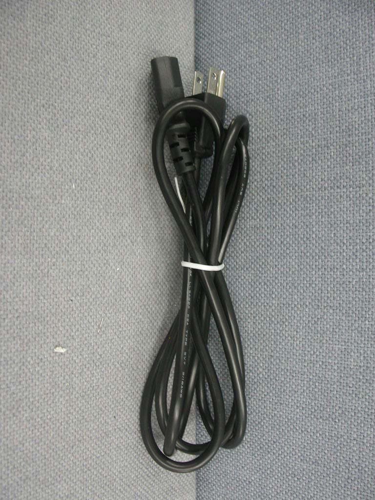
PL4CT1810
Sep 25, 2002LCD Monitor
Equipment Class
JBP - Part 15 Class B Computing Device Peripheral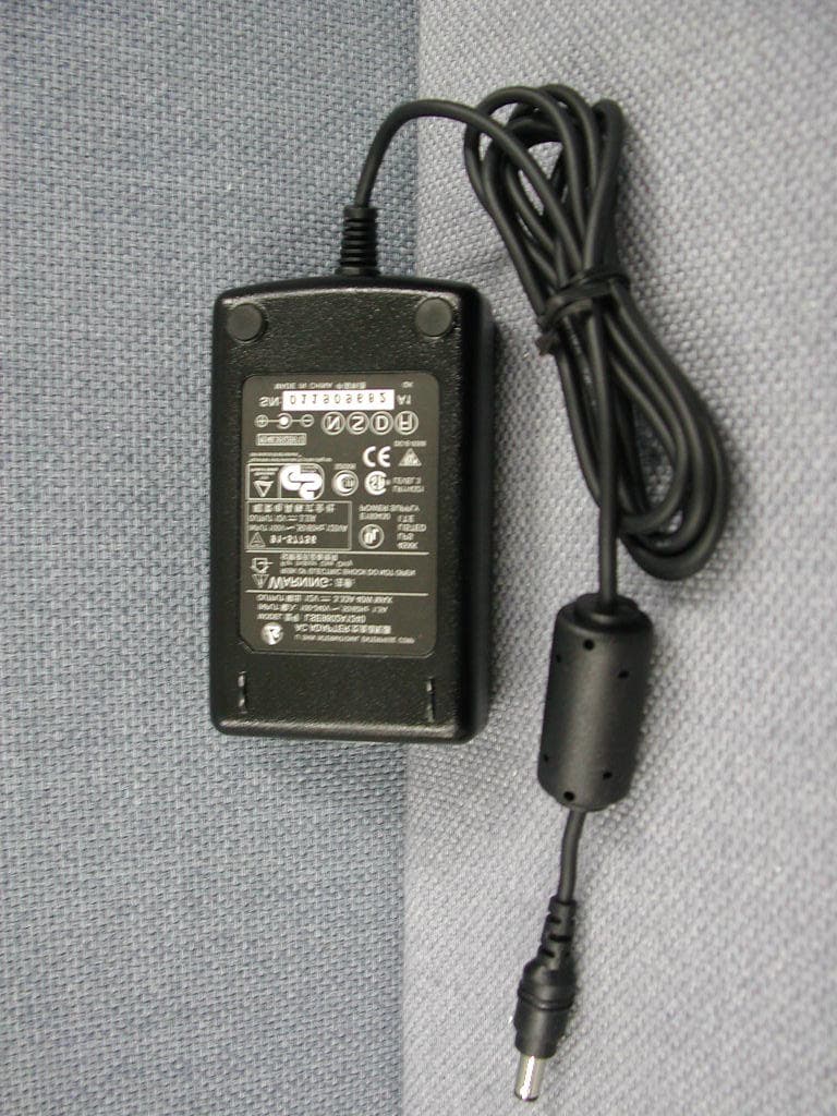
PL4CT1701
Mar 21, 200217-inch LCD Monitor
Equipment Class
JBP - Part 15 Class B Computing Device Peripheral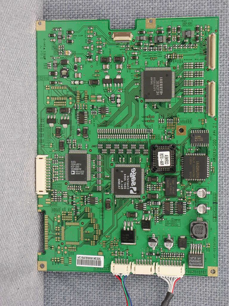
PL4CT1501
Nov 11, 200115-inch LCD Monitor
Equipment Class
JBP - Part 15 Class B Computing Device Peripheral