PLVSDTX-ARK620 Watt Multimode SDR Transmitter
Screen Service Broadcasting Technologies SpA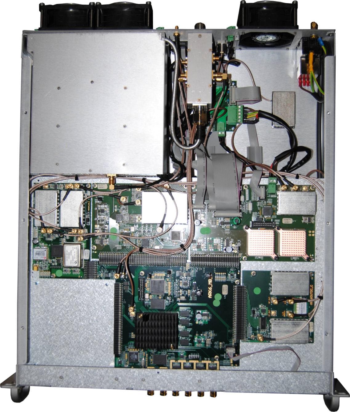
Click to zoom
Application Details
- Equipment Class
- TBC - Licensed Broadcast Station Transmitter
- Date of Grant
- Jun 06, 2012
- Application Purpose
- Original Equipment
- Date of Application
- Mar 15, 2012
- Equipment Note
- 20 Watt Multimode SDR Transmitter
- Frequency Range
- 614.00000000 - 698.00000000
- Country
- Italy
Documents & Files
Document Text
Text extracted from the exhibit documents filed with the FCC. Open a document above to read the original.
Users Manual
ISO 9001:2000 Cert. N°4500/1 Document name: SDT_ARK6_User_Manual_ENG_vATSC Document code: ARK6-UM-000 Author: C. Di Biase Date: September 23rd, 2011 Version: 1.1 Software User Manual ARK6 External Document ISO 9001:2000 Cert. N°4500/1 Version 1.1 SDT_ARK6_User_Manual_ENG_vATSC Page 2 of 206 Table of Contents 1 Document structure ............................................................................................................... 5 2 Scope of the document .......................................................................................................... 6 3 Introduction ........................................................................................................................... 7 3.1 Digitizer features .............................................................................................................. 9 3.2 Satellite receivers features ............................................................................................... 9 3.2.1 DVB-S/S2 .................................................................................................................. 9 3.2.2 DVB-S/S2 plus CAM ............................................................................................... 10 3.3 Terrestrial receivers features ......................................................................................... 11 3.3.1 ATSC ....................................................................................................................... 11 3.4 ITU Transmitter features ................................................................................................ 12 3.4.1 ITU Features........................................................................................................... 12 3.4.2 ITU Signal Processing ............................................................................................. 13 3.5 ATSC Transmitter features ............................................................................................. 14 3.5.1 ATSC Features ........................................................................................................ 14 3.5.2 ATSC Signal Processing .......................................................................................... 14 3.6 System Features ............................................................................................................. 15 3.7 Synchronization .............................................................................................................. 15 4 Specifications ....................................................................................................................... 16 4.1 Input Interfaces .............................................................................................................. 16 4.2 Output Interfaces ........................................................................................................... 19 4.3 Control Interfaces ........................................................................................................... 22 4.3.1 RS232 pinout ......................................................................................................... 23 4.3.2 TLC pinout .............................................................................................................. 23 4.3.3 TLS pinout .............................................................................................................. 24 4.4 Power Supply .................................................................................................................. 25 4.5 Environmental Specification .......................................................................................... 27 4.6 Mechanical Specification................................................................................................ 27 5 Java Graphic User Interface ................................................................................................. 28 5.1 Authentication Option ................................................................................................... 28 5.2 Java Menu Bar ................................................................................................................ 29 5.3 Home Page ..................................................................................................................... 31 5.4 Input ............................................................................................................................... 32 5.5 Front-End ........................................................................................................................ 37 5.5.1 Tuner window: RF power level monitor ................................................................ 38 ISO 9001:2000 Cert. N°4500/1 Version 1.1 SDT_ARK6_User_Manual_ENG_vATSC Page 3 of 206 5.5.2 DIGITIZER FE Type .................................................................................................. 39 5.5.3 ATSC FE Type ......................................................................................................... 41 5.6 ATSC ............................................................................................................................... 44 5.6.1 ATSC Settings ......................................................................................................... 45 5.6.2 ATSC Modulation ................................................................................................... 49 5.6.3 ATSC TVCT .............................................................................................................. 51 5.6.4 ATSC Measure ........................................................................................................ 52 5.7 ITU.470 ........................................................................................................................... 54 5.7.1 ITU Settings ................................................................................…
Text truncated - open the document above for the full version.
Block Diagram
SDT 500 UB ARK 6_ATSC_FCC SW BLOCK DIAGRAM V 1.0 Page 1 - 1 SDT 500 UB ARK 6 FCC Software Block Diagram SDT 500 UB ARK 6_ATSC_FCC SW BLOCK DIAGRAM V 1.0 Page 1 - 2 CONTENTS 1.1 INTRODUCTION .................................................................................................................................... 3 1.2 BLOCK DIAGRAM .................................................................................................................................. 3 1.3 BLOCK DESCRIPTION .......................................................................................................................... 4 SDT 500 UB ARK 6_ATSC_FCC SW BLOCK DIAGRAM V 1.0 Page 1 - 3 1.1 INTRODUCTION This note describes the high level software architecture. For each block only few sentence will be given. More detailed description will be provided if required 1.2 BLOCK DIAGRAM FILE SYSTEM MANAGEMENT EXTERNAL UART MANAGEMENT COMMUNICATION MANAGEMENT TLC MANAGEMENT TLS MANAGEMENT TCP MANAGEMENT SNMP MANAGEMENT DISPLAY MANAGEMENT MAIN PROGRAM SDT 500 UB ARK 6_ATSC_FCC SW BLOCK DIAGRAM V 1.0 Page 1 - 4 1.3 BLOCK DESCRIPTION 1 MAIN PROGRAM Initialize the System at the Switch On By the operative system it manages the tasks hereunder described. The tasks run all in parallel mode: a) FILE SYSTEM MANAGEMENT o Management of the configuration files o Any save transmitter action creates a file to be saved o Any reload transmitter action o Any parameters modification transmitter action b) EXTERNAL UART MANAGEMENT o By a proprietary protocol it manages, via serial line (232 level), all the W/R equipment registers c) COMMUNICATION MANAGEMENT o Communication management between microprocessor and the function forming the equipment: o Up converter o Down converter o Modulator d) TLC MANAGEMENT o It manages by the opto (four) the whole equipment o RF on/off o Remote standby o Change mode o Alarm reset e) TLS MANAGEMENT o It manages by the relais (four) the whole equipment o RF on/off (or selected alarm) o Mode selcted (or selected alarm) o Alarm defined by web interface mask (two relais) f) TCP MANAGEMENT o Communication management between microprocessor and web interface: o Micro answer to java request g) SNMP MANAGEMENT o It manages by snmp protocol the following standard SNMP operations o Get operation o Get next operation o Walk operation o Set operation o Trap h) DISPLAY MANAGEMENT o By a communication protocol between main micro and display micro it manages the following operations: o Menu Navigation o Data Settings o Data Refresh
Block Diagram
SDT 201 UB ARK 6_ATSC_FCC SW BLOCK DIAGRAM V 1.0 Page 1 - 1 SDT 201 UB ARK 6 FCC Software Block Diagram SDT 201 UB ARK 6_ATSC_FCC SW BLOCK DIAGRAM V 1.0 Page 1 - 2 CONTENTS 1.1 INTRODUCTION .................................................................................................................................... 3 1.2 BLOCK DIAGRAM .................................................................................................................................. 3 1.3 BLOCK DESCRIPTION .......................................................................................................................... 4 SDT 201 UB ARK 6_ATSC_FCC SW BLOCK DIAGRAM V 1.0 Page 1 - 3 1.1 INTRODUCTION This note describes the high level software architecture. For each block only few sentence will be given. More detailed description will be provided if required 1.2 BLOCK DIAGRAM FILE SYSTEM MANAGEMENT EXTERNAL UART MANAGEMENT COMMUNICATION MANAGEMENT TLC MANAGEMENT TLS MANAGEMENT TCP MANAGEMENT SNMP MANAGEMENT DISPLAY MANAGEMENT MAIN PROGRAM SDT 201 UB ARK 6_ATSC_FCC SW BLOCK DIAGRAM V 1.0 Page 1 - 4 1.3 BLOCK DESCRIPTION 1 MAIN PROGRAM Initialize the System at the Switch On By the operative system it manages the tasks hereunder described. The tasks run all in parallel mode: a) FILE SYSTEM MANAGEMENT o Management of the configuration files o Any save transmitter action creates a file to be saved o Any reload transmitter action o Any parameters modification transmitter action b) EXTERNAL UART MANAGEMENT o By a proprietary protocol it manages, via serial line (232 level), all the W/R equipment registers c) COMMUNICATION MANAGEMENT o Communication management between microprocessor and the function forming the equipment: o Up converter o Down converter o Modulator d) TLC MANAGEMENT o It manages by the opto (four) the whole equipment o RF on/off o Remote standby o Change mode o Alarm reset e) TLS MANAGEMENT o It manages by the relais (four) the whole equipment o RF on/off (or selected alarm) o Mode selcted (or selected alarm) o Alarm defined by web interface mask (two relais) f) TCP MANAGEMENT o Communication management between microprocessor and web interface: o Micro answer to java request g) SNMP MANAGEMENT o It manages by snmp protocol the following standard SNMP operations o Get operation o Get next operation o Walk operation o Set operation o Trap h) DISPLAY MANAGEMENT o By a communication protocol between main micro and display micro it manages the following operations: o Menu Navigation o Data Settings o Data Refresh
Block Diagram
SCREEN SERVICE BROADCASTING TECHNOLOGIES VIA Giuseppe Di Vittorio, 17 25 125 BRESCIA, ITALIA 1 FUNCTIONAL BLOCK DIAGRAM Screen Service Functional Block Diagram Purpose July, 2009 v 1.0 Page 1 - 2 1.1 FUNCTIONAL BLOCK DIAGRAM BOARD MODE SELECTOR RF IN DOWNCONVERTER IF IN 36 MHz ALARM PROCESSOR EVENT PROCESSOR RELAYS MANAGEMENT SNMP TRAP PROCESSOR GbE MANAGEMENT RELAYS AM/PM PRECORRECTION RF Output AMPLIFIER AMPL PWR OFF UPCONVERTER CHANNEL RF 1 PPS external 10 MHz external GPS input GPS Rx CLOCK SELECTION 10 M & 1 PPS GPS 10 M & 1 PPS ATSC Modulator ITU470 Modulator SDI Input 1 SDI Input 2 ATSC MODE ALARMS UPCONVERTER ALARMS CLOCK ALARMS AMPLI/POWER ALARMS SYSTEM ALARMS DOWNCONVERTER ALARMS ALARMS DETECTION Board mode Management OPTO RS 232 LOCAL INTERFACE COMMANDS MAILBOX SNMP SERVER JAVA SERVER OPTO INPUT MANAGEMENT STAND-BY STAND-BY Processor STD-BY command NETWORK MANAGEMENT COMMANDS PROCESSOR SNMP SERVER JAVA SERVER MANAGEMENT COMMANDS RESET COMMANDS OPTO command EVENTS Monitoring IF OUT GPS unlocked alarm 10MHz unlocked alarm GPS communication error alarm 129 MHz unlocked alarm 960 MHz unlocked alarm Down-conv. oscillator unlock alarm Rf input Squelch alarm File system error alarm Bad file in file system alarm No TS Input Up-conv. oscillator unlocked alarm Up-conv commmunication error alarm PSU voltage out of range alarm PSU current out of range alarm High case temperature alarm Absolute power limiter alarm Case temperature warning Case temperature alarm High forward power alarm Low forward power warning Low forward power alarm High reflected power alarm FAN speed alarm AMPLI POWER ALARMS UPCONVERTER ALARMS ATSC MODE ALARMS SYSTEM ALARMS DOWNCONVERTER ALARMS CLOCK ALARMS Warm UP Alarm FPGA Boot Alarm RX ATSC ALARMS ASI output ASI/SSI Input 1 GBe Input ASI/SSI Input 2 ASI/SSI Input 3 ASI/SSI Input 4 ADAPTIVE FILTER I/Q base band IF to AM/PM PRECORRECTION No SDI Input ITU 470 MODE ALARMS Wrong input standard
External Photos
1 SDT 201 UB ARK 6_PICTURE CONTENTS 1.1 PURPOSE .............................................................................................................................................. 3 1.2 COMPOSITION ...................................................................................................................................... 3 1. AGILE DOWN CONVERTER _NOT EQUIPPED .................................................................................. 3 2. DIGITAL CORE ..................................................................................................................................... 3 3. UP CONVERTER .................................................................................................................................. 3 4. FREQ. REF. ........................................................................................................................................... 3 5. MEAS & PRECORRECTION ................................................................................................................. 3 6. TLS/TLC & RF DETECTOR .................................................................................................................. 3 7. RF POWER AMPLI ................................................................................................................................ 3 8. FAN BOARD .......................................................................................................................................... 3 9. OUPUT COUPLER ................................................................................................................................ 3 10. RF DRIVER AMPLI ............................................................................................................................ 3 11. POWER SUPPLY .............................................................................................................................. 3 1.3 PICTURE ................................................................................................................................................ 5 1.1 PURPOSE The document purpose is to give the sufficient and necessary informations about the SCHEMATIC of the equipment 1.2 COMPOSITION The equipment is composed of the following functional blocks: 1. AGILE DOWN CONVERTER _NOT EQUIPPED 2. DIGITAL CORE 3. UP CONVERTER 4. FREQ. REF. 5. MEAS & PRECORRECTION 6. TLS/TLC & RF DETECTOR 7. RF POWER AMPLI 8. FAN BOARD 9. OUPUT COUPLER 10. RF DRIVER AMPLI 11. POWER SUPPLY 1 2 3 4 5 6 7 8 9 10 11 1.3 PICTURE 1. Open Top Vieview 2. Front Vieview 3. Rear Vieview 4. Right Side Vieview 1. Left Side Vieview AGILE DOWN CONVERTER
ID Label/Location Info
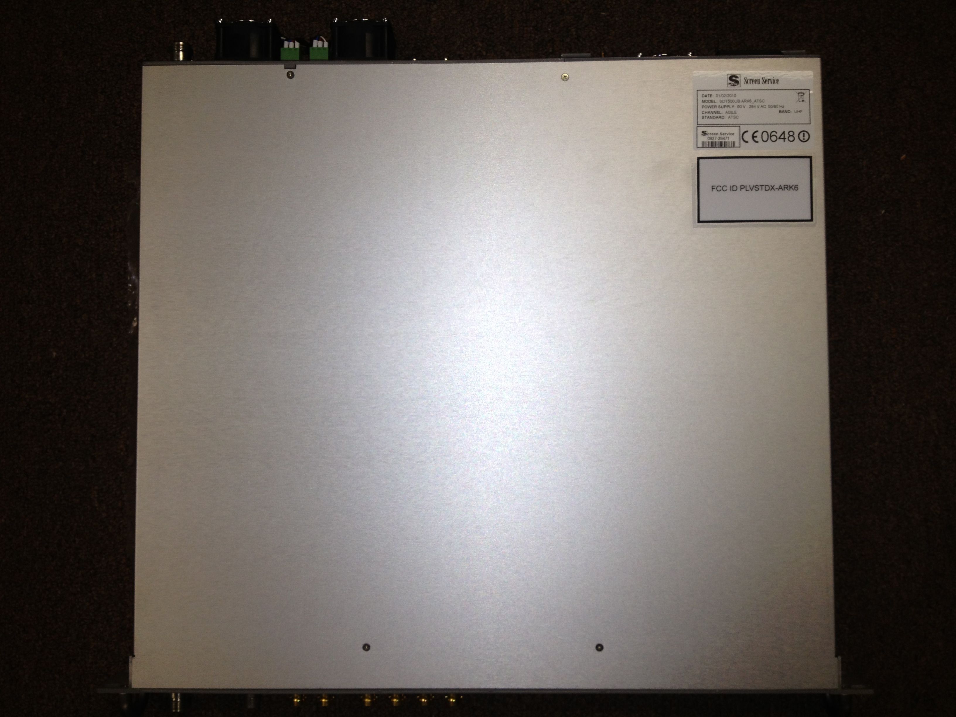
FCC ID PLVSTDX-ARK6 FCC ID PLVSTDX-ARK6 FCC ID PLVSTDX-ARK6 FCC ID PLVSTDX-ARK6 FCC ID PLVSTDX-ARK6 FCC ID PLVSTDX-ARK6 FCC ID PLVSTDX-ARK6 FCC ID PLVSTDX-ARK6 FCC ID PLVSTDX-ARK6 FCC ID PLVSTDX-ARK6
Internal Photos
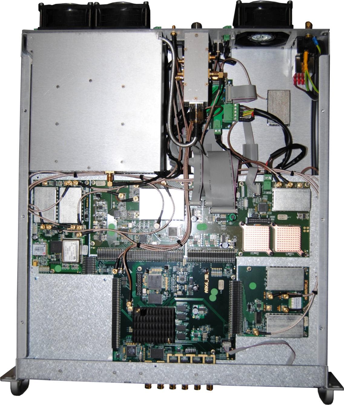
1 SDT 500 UB ARK 6_PICTURE CONTENTS 1.1 PURPOSE .............................................................................................................................................. 3 1.2 COMPOSITION ...................................................................................................................................... 3 1.3 PICTURE ................................................................................................................................................ 5 1.3.1 Open Top Vieview ............................................................................................................................. 5 1.3.2 Front Vieview .................................................................................................................................... 6 1.3.3 Rear Vieview ..................................................................................................................................... 6 1.3.4 Right Side Vieview ............................................................................................................................ 6 1.3.1 Left Side Vieview ............................................................................................................................. 6 1.1 PURPOSE This brief document details the board included in the equipment tested for FCC purpose. 1.2 COMPOSITION The equipment is composed of the following functional blocks: 1 st POWER SUPPLY 2 nd ARK 6 FRONT END (not equipped) 3 rd ARK 6 DIGITAL CORE 4 th ARK 6 UP CONVERTER 5 TH ARK 6 FREQUENCY REFERENCE 6 TH ARK 6 MEASURE & PRECORRECTION 7 TH PS & TLC/TLS & RF DETECTOR 8 th RF POWER AMP 9 TH FAN & TEMPERATURE SENSOR 2_ARK 6 FRONT END NOT EQUIPPED 5_ARK 6 FREQ. REF. 6_ARK 6 MEASURE & PRECORRECTION 3_ARK 6 DIGITAL CORE 4_ARK 6 UP CONVERTER 7_PS & TLC/TLS & RF DETECTOR 8_RF POWER AMP 1_ PSU 9_FAN & TEMP SENSOR 1A__MOTHERBOARD 1.3 PICTURE 1.3.1 Open Top View 1.3.2 Front View 1.3.3 Rear View 1.3.4 Right Side View 1.3.1 Left Side View
Operational Description
SCREEN SERVICE BROADCASTING TECHNOLOGIES VIA Giuseppe Di Vittorio, 17 25 125 BRESCIA, ITALIA Pagina 1 di 3 1 OPERATIONAL DESCRIPTION SCREEN SERVICE BROADCASTING TECHNOLOGIES VIA Giuseppe Di Vittorio, 17 25 125 BRESCIA, ITALIA Pagina 2 di 3 CONTENTS 1.1 PURPOSE .............................................................................................................................................. 3 SCREEN SERVICE BROADCASTING TECHNOLOGIES VIA Giuseppe Di Vittorio, 17 25 125 BRESCIA, ITALIA Pagina 3 di 3 1.1 Operational Description The SDTx ARK6 Transmitter is composed of a sophisticated software controlled ATSC exciter, a linear UHF amplifier, and emission masks filter. The ATSC exciter is an ATSC professional exciter, designed for the most demanding digital broadcasting applications. It receives the input transport stream and processes the signal. It integrates a modulator module that incorporates modulus/group delay software precorrection as well as AM/PM software precorrection for the power amplifier and emission mask filter. Very high linearity performance is possible thanks to very careful RF design over the entire UHF band and with an optimal digital precorrection engine working simultaneously in the time and frequency domains. A high degree of reliability is guaranteed, moreover, by the use of four amplifiers operating in parallel and softfail operation. Multiple power supplies are operated in parallel to reduce the possibility of single-point failure modes. Also, multiple cooling fans are used to keep the operational temperature of critical components Due to the unique design, the transmitter amplifier is suitable to any digital TV standard: ATSC, ATSC-MH, ISDB-T, DVB-T, DVB-H and DMB-T. It is only necessary to reconfigure the modulator and use the appropriate RF output band pass filter. The remaining components may be used without any change. The emission mask filter is a low-loss filter that reduces the out-of-channel radiation to limits that are acceptable to prevent interference to other services and eliminate harmonic radiation.
Parts List/Tune Up Info
SCREEN SERVICE BROADCASTING TECHNOLOGIES VIA Giuseppe Di Vittorio, 17 25 125 BRESCIA, ITALIA Pagina 1 di 7 TUNE –UP PROCEDURE SDT 500 UB ARK 6 SCREEN SERVICE BROADCASTING TECHNOLOGIES VIA Giuseppe Di Vittorio, 17 25 125 BRESCIA, ITALIA Pagina 2 di 7 CONTENTS 1.1 PURPOSE .............................................................................................................................................. 3 1.2 CHANNEL SETTING ............................................................................................................................. 4 1.3 OUTPUT POWER SETTING .................................................................................................................. 5 1.4 INPUT SELECTION ................................................................................................................................ 6 1.5 THRESHOLD SELECTION ................................................................................................................... 7 SCREEN SERVICE BROADCASTING TECHNOLOGIES VIA Giuseppe Di Vittorio, 17 25 125 BRESCIA, ITALIA Pagina 3 di 7 1.1 PURPOSE The document purpose is to give the sufficient and necessary information about: Final stage_AB driver stage_A pre driver stage_A VDC 24 V VDC 3.4 V VDC 3.7 V FINAL STAGES CURRENT VALUES ARE SLIGHTLY FREQUENCY DEPENDANT Power Consumption at quiscent Polarization Voltage 0.145 ± 0.005V Pre driver GREY 1.6 ± 0.1A 0.275 ± 0.005V Driver BLACK 0.275 ± 0.005V Driver BLACK SCREEN SERVICE BROADCASTING TECHNOLOGIES VIA Giuseppe Di Vittorio, 17 25 125 BRESCIA, ITALIA Pagina 4 di 7 1.2 CHANNEL SETTING The channel setting operations are the following: 1. Connect the equipment by the front TCP/IP connector to the LAP TOP using the IP address shown by the front display. The following alternatives will appears 2. Once connected select the window(ON THE LEFT) to select to change the output channel Push down arrow and select the channel: 3. Save the new setting by pushing SCREEN SERVICE BROADCASTING TECHNOLOGIES VIA Giuseppe Di Vittorio, 17 25 125 BRESCIA, ITALIA Pagina 5 di 7 1.3 OUTPUT POWER SETTING The output power setting (MAX POWER in ATSC MODE is 20 W = 43 dBm) operations are the following: 1. Connect the equipment by the front TCP/IP connector to the LAP TOP using the IP address shown by the front display. The following alternatives will appears 2. Once connected select the window to select to change the output power There are two possible option: a. in dBm (in this case the max value will be 43) b. in W ( in this case the max value will be 20) 3. Save the new setting by pushing SCREEN SERVICE BROADCASTING TECHNOLOGIES VIA Giuseppe Di Vittorio, 17 25 125 BRESCIA, ITALIA Pagina 6 di 7 1.4 INPUT SELECTION To select the input please operate as follows: 1. Connect the equipment by the front TCP/IP connector to the LAP TOP using the IP address shown by the front display. The following alternatives will appears 2. Once connected select the window 3. Select INPUT SELECTOR and by pushing the down arrow choose the defined input mode 4. Save the new setting by pushing SCREEN SERVICE BROADCASTING TECHNOLOGIES VIA Giuseppe Di Vittorio, 17 25 125 BRESCIA, ITALIA Pagina 7 di 7 1.5 THRESHOLD SELECTION The to select the FORWARD and TEMPERATURE threshold please operate as follows: 1. Connect the equipment by the front TCP/IP connector to the LAP TOP using the IP address shown by the front display. The following alternatives will appears 2. Once connected select the window 3. Select the FWD power THRESHOLD and select the Alarm level and the Warning level. 4. Select the Temperature THRESHOLD and select the Alarm level and the Warning level. 5. Save the new setting by pushing
Schematics
PAC101 PAC102 COC1 PAC201PAC202 COC2 PAC301 PAC302 COC3 PAC401PAC402 COC4 PAC501PAC502 COC5 PAC602PAC601 COC6 PADZ101PADZ102 CODZ1 PAFid10FIDU COFid1 PAFid20FIDU COFid2 PAFid40FIDU COFid4 PAIC103 PAIC104PAIC101PAIC105PAIC102 COIC1 PAIC201 PAIC202 PAIC203 PAIC204PAIC205 PAIC206 PAIC207 PAIC208 COIC2 PAJ101PAJ103PAJ105PAJ107PAJ109 PAJ102PAJ104PAJ106PAJ108PAJ1010 PAJ100 COJ1 PAJ208PAJ207 PAJ206PAJ205 PAJ204PAJ203 PAJ2010PAJ209 PAJ202PAJ201 COJ2 PAP100 COP1 PAP200 COP2 PAP300 COP3 PAQ101 PAQ102PAQ103 COQ1 PAR101 PAR102 COR1 PAR201PAR202 COR2 PAR301PAR302 COR3 PAR401PAR402 COR4 PAR502 PAR501 COR5 PAC102 PAC601 PAIC103 PAJ101PAJ103PAJ105PAJ107PAJ109 PAP100 PAR201 PAR402 PAC302 PAC401 PADZ102 PAIC208 PAQ103 PAR202 PAC202 PAC502 PAIC105 PAP300 PAJ201 PAJ204 PAJ206 PAJ208PAJ207 PAQ102 PAJ203 PAJ205 PAC101 PAC201 PAC301 PAC402 PAC501 PAC602 PADZ101 PAIC101 PAIC204PAIC205 PAJ100 PAJ102PAJ104PAJ106PAJ108PAJ1010 PAJ209 PAP200 PAR302 PAIC201 PAIC202 PAJ202 PAR502 PAIC102 PAR101 PAIC104 PAIC203 PAR301 PAR501 PAIC206 PAIC207 PAQ101 PAR102 PAJ2010 PAR401 PAC101 PAC102 COC1 PAC201PAC202 COC2 PAC301 PAC302 COC3 PAC401PAC402 COC4 PAC501PAC502 COC5 PAC602PAC601 COC6 PADZ101PADZ102 CODZ1 PAFid10FIDU COFid1 PAFid20FIDU COFid2 PAFid40FIDU COFid4 PAIC103 PAIC104PAIC101PAIC105PAIC102 COIC1 PAIC201 PAIC202 PAIC203 PAIC204PAIC205 PAIC206 PAIC207 PAIC208 COIC2 PAJ101PAJ103PAJ105PAJ107PAJ109 PAJ102PAJ104PAJ106PAJ108PAJ1010 PAJ100 COJ1 PAJ208PAJ207 PAJ206PAJ205 PAJ204PAJ203 PAJ2010PAJ209 PAJ202PAJ201 COJ2 PAP100 COP1 PAP200 COP2 PAP300 COP3 PAQ101 PAQ102PAQ103 COQ1 PAR101 PAR102 COR1 PAR201PAR202 COR2 PAR301PAR302 COR3 PAR401PAR402 COR4 PAR502 PAR501 COR5 PAC102 PAC601 PAIC103 PAJ101PAJ103PAJ105PAJ107PAJ109 PAP100 PAR201 PAR402 PAC302 PAC401 PADZ102 PAIC208 PAQ103 PAR202 PAC202 PAC502 PAIC105 PAP300 PAJ201 PAJ204 PAJ206 PAJ208PAJ207 PAQ102 PAJ203 PAJ205 PAC101 PAC201 PAC301 PAC402 PAC501 PAC602 PADZ101 PAIC101 PAIC204PAIC205 PAJ100 PAJ102PAJ104PAJ106PAJ108PAJ1010 PAJ209 PAP200 PAR302 PAIC201 PAIC202 PAJ202 PAR502 PAIC102 PAR101 PAIC104 PAIC203 PAR301 PAR501 PAIC206 PAIC207 PAQ101 PAR102 PAJ2010 PAR401 PAC101 PAC102 COC1 PAC201PAC202 COC2 PAC301 PAC302 COC3 PAC401PAC402 COC4 PAC501PAC502 COC5 PAC602PAC601 COC6 PADZ101PADZ102 CODZ1 PAFid10FIDU COFid1 PAFid20FIDU COFid2 PAFid40FIDU COFid4 PAIC103 PAIC104PAIC101PAIC105PAIC102 COIC1 PAIC201 PAIC202 PAIC203 PAIC204PAIC205 PAIC206 PAIC207 PAIC208 COIC2 PAJ101PAJ103PAJ105PAJ107PAJ109 PAJ102PAJ104PAJ106PAJ108PAJ1010 PAJ100 COJ1 PAJ208PAJ207 PAJ206PAJ205 PAJ204PAJ203 PAJ2010PAJ209 PAJ202PAJ201 COJ2 PAP100 COP1 PAP200 COP2 PAP300 COP3 PAQ101 PAQ102PAQ103 COQ1 PAR101 PAR102 COR1 PAR201PAR202 COR2 PAR301PAR302 COR3 PAR401PAR402 COR4 PAR502 PAR501 COR5 PAC102 PAC601 PAIC103 PAJ101PAJ103PAJ105PAJ107PAJ109 PAP100 PAR201 PAR402 PAC302 PAC401 PADZ102 PAIC208 PAQ103 PAR202 PAC202 PAC502 PAIC105 PAP300 PAJ201 PAJ204 PAJ206 PAJ208PAJ207 PAQ102 PAJ203 PAJ205 PAC101 PAC201 PAC301 PAC402 PAC501 PAC602 PADZ101 PAIC101 PAIC204PAIC205 PAJ100 PAJ102PAJ104PAJ106PAJ108PAJ1010 PAJ209 PAP200 PAR302 PAIC201 PAIC202 PAJ202 PAR502 PAIC102 PAR101 PAIC104 PAIC203 PAR301 PAR501 PAIC206 PAIC207 PAQ101 PAR102 PAJ2010 PAR401 PAC101 PAC102 COC1 PAC201PAC202 COC2 PAC301 PAC302 COC3 PAC401PAC402 COC4 PAC501PAC502 COC5 PAC602PAC601 COC6 PADZ101PADZ102 CODZ1 PAFid10FIDU COFid1 PAFid20FIDU COFid2 PAFid40FIDU COFid4 PAIC103 PAIC104PAIC101PAIC105PAIC102 COIC1 PAIC201 PAIC202 PAIC203 PAIC204PAIC205 PAIC206 PAIC207 PAIC208 COIC2 PAJ101PAJ103PAJ105PAJ107PAJ109 PAJ102PAJ104PAJ106PAJ108PAJ1010 PAJ100 COJ1 PAJ208PAJ207 PAJ206PAJ205 PAJ204PAJ203 PAJ2010PAJ209 PAJ202PAJ201 COJ2 PAP100 COP1 PAP200 COP2 PAP300 COP3 PAQ101 PAQ102PAQ103 COQ1 PAR101 PAR102 COR1 PAR201PAR202 COR2 PAR301PAR302 COR3 PAR401PAR402 COR4 PAR502 PAR501 COR5 PAC102 PAC601 PAIC103 PAJ101PAJ103PAJ105PAJ107PAJ109 PAP100 PAR201 PAR402 PAC302 PAC401 PADZ102 PAIC208 PAQ103 PAR202 PAC202 PAC502 PAIC105 PAP300 PAJ201 PAJ204 PAJ206 PAJ208PAJ207 PAQ102 PAJ203 PAJ205 PAC101 PAC201 PAC301 PAC402 PAC501 PAC602 PADZ101 PAIC101 PAIC204PAIC205 PAJ100 PAJ102PAJ104PAJ106PAJ108PAJ1010 PAJ209 PAP200 PAR302 PAIC201 PAIC202 PAJ202 PAR502 PAIC102 PAR101 PAIC104 PAIC203 PAR301 PAR501 PAIC206 PAIC207 PAQ101 PAR102 PAJ2010 PAR401
Schematics
1 FL ASH_A25 1 VI RTE X_BUSY 1 HS W A P_E N 1 CCLK 1 RDW R_B 1 VI RTE X_DONE 1 FL ASH_R\ S\T\ 1 Ne t TP 144 _1 1 ARM - A3 1 ARM - A6 1 ARM - A12 1 ARM - A16 4 2TM S 1 FL ASH__R\S\ T\2\ 1 LED2- 0 1 LED2- 1 1 1M DC 1 CONFI G_0 1 CONFI G_1 1 ARM - D3 1 ARM CK 1 R\ S\ T\ - PSU 1 ARM - A25 1 Ne t TP 141 _1 1 NM EA _TX 1 NM EA _RX 1 ARM - A2 1 RS 232 TTL - RX 1 SDI O 1 ARM _ \ W \ E\ 1 1 CS B 1 R\ S\ T \ 1 I2C_SDA 1 ARM - A4 1 GB ETH_RS T 1 ARM - A8 1 DI SPL AY - RX 1 ARM - A14 1 ARM - A18 1 10M _EX 1 ARM - D1 1 ARM _ R\ D\ 1 ARM - A10 4B MDI1+ 1A 2M DI 0- 9A 1V8GA1 1 SDO4 1 AUX1 1 VBATT1 1 AUX3 1 AUX5 1 WAIT0 1 RT CXTO 1 R\ S\ T \ 1 Net TP97_1 1 Ne t TP 101 _1 1 Ne t TP 104 _1 1 CKOUT 18 GND 14 GND 16 GND 1 ARM - D13 1 ARM - D9 1 FPGA- CS 1 ARM - D11 1 GB _FR AM E- R DY 12 GND 10 GND 8 GND 1 ARM - A1 1 US B+ 4 GND 2 +3 . 3 V 1 GND 1 NC 4 Net D20_A 3 Ne t J P 5_3 14A +2 . 5 V 12A +2 . 5 V 12B +2 . 5 V 11B Ne t J 5 _11 B 0 3B MDI1- 5B MDI2- 2B MDI0+ 6B MDI2+ 9B 1V8GA1 8B MDI3+ 10BGND 8A 2M DI 3+ 6A 2M DI 2+ 4A 2M DI 1+ 7A 2M DI 3- 5A 2M DI 2- 10AGND 1 A\ S\ I \ _\ O\ U\ T\ _LP 1 AS I _OUT_ HP 1 A\ S\ I \ _\ O\ U\ T\ _HP 7 2TDO SHLD2 GND 0 GND 0 GND 1 SDO1 1 S\ D\ O\1 1 SDO2 1 S\ D\ O\2 1 S\ D\ O\4 1 FL ASH_W AIT1 1 FL ASH_CK 1 FL ASH-A\ D\V\2 6 2TDI 5 2TCK 1 Ne t TP 146 _1 1 NOBL I NK 4 TDO 5 TDI 1 +2 . 5 V 2 GND 1 FL ASH_O\ E\ 2 +1 . 8 V 1 GND 1 1M DI O 1 LED_LINK0 1 ACTI VI TY0 1 LED_LINK1 1 ACTI VI TY 1 1 CONFI G_2 1 CONFI G_3 1 CONFI G_4 1 CONFI G_5 1 1GRXD0 1 1GRXD1 1 2GTXD2 1 2GTXD3 1 1GTXD0 1 1GTXD1 1 1GTXD2 1 1GTXD3 1 2GRXD0 1 2GRXD1 4 FE_P0 6 FE_P1 8 +5 . 5 V 2 RX 4 GND 6 +5 . 5 V 2 GND 3 DI SPL AY - RX 1 54M HZ 10 FE_P2 12 FE_P3 14 FE_P4 1 AUX_P 35 1 AUX_P 38 1 AUX0 18 GND 20 FE_P6 55 GND 57 OUTDC- ATT- CLK 1 AUX15 1 D_ I N_ 1 1 AUX2 26 FE_P9 24 FE_P8 51 AUX_N36 49 GND 47 AUX_N35 32 GND 30 FE_P11 41 AUX_N33 43 GND 45 AUX_N34 40 FE_P15 38 FE_P14 36 FE_P13 35 AUX_N31 37 GND 1 SOFT- START15 4 GND 46 GND 44 FE_P17 42 FE_P16 29 AUX_N29 31 GND 5 GND 3 GND 50 FE_P19 52 FE_PHR 23 AUX_N27 25 GND 4 GND 56 FE_TTL2 58 GND 19 …
Text truncated - open the document above for the full version.
Contact Information
Applicant
Graziano Casale(Sales Director)
Technical Contact
Screen Service America, LLCFernando J. Grullon
[email protected]305-826-2212
6095 NW 167th Street · Hialeah, Florida · United States
Non-Technical Contact
Screen Service America, LLCVailma Roca
[email protected]305-826-2212
Technical Specifications
| # | Rule Parts | Frequency Range | Power Output | Emission | Tolerance |
|---|---|---|---|---|---|
| 2 | 74 | 614 MHz - 698 MHz | 20 W | 6M00C7W | 250 Hz |
Other Applications from Screen Service Broadcasting Technologies SpA
PLVSDT201UB-ARK6
Jun 04, 2012125 Watt Multimode SDR Transmitter
Equipment Class
TBC - Licensed Broadcast Station Transmitter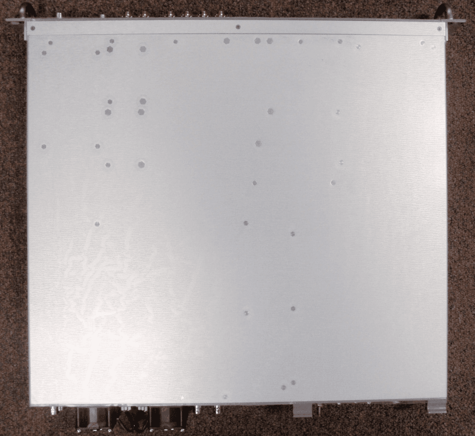
PLVSTDX-ARK-ECHO
Jan 19, 201220 Watt Multimode SDR Repeater w/ Echo Cancellation
Equipment Class
TBC - Licensed Broadcast Station Transmitter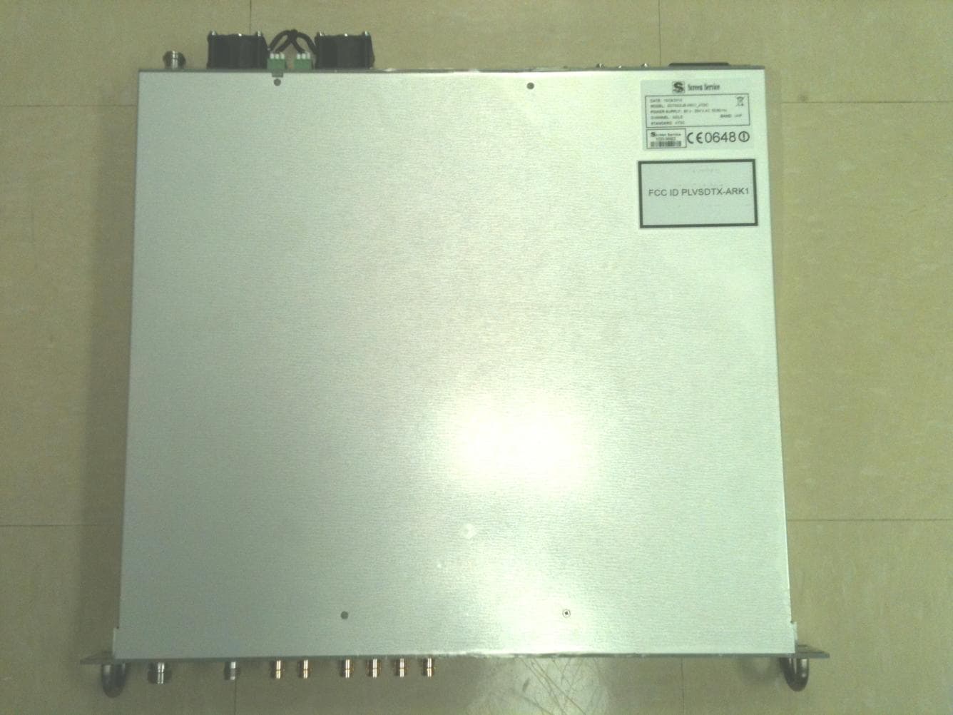
PLVSDTX-ARK1
Aug 22, 201120 Watt Multimode SDR Transmitter
Equipment Class
TBC - Licensed Broadcast Station Transmitter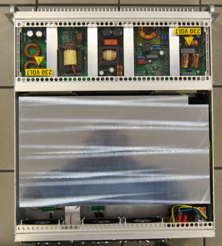
PLVSDT501UBCARK1T
Jan 20, 2011200 Watt Multimode SDR Transmitter
Equipment Class
TNB - Licensed Non-Broadcast Station Transmitter