PQ4IPROA3Mobile Phone
HONG KONG IPRO TECHNOLOGY CO.,LIMITED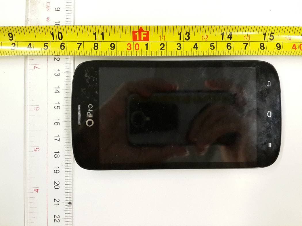
Click to zoom
Application Details
- Equipment Class
- DTS - Digital Transmission System
- Date of Grant
- Dec 26, 2013
- Application Purpose
- Original Equipment
- Date of Application
- Dec 26, 2013
- Equipment Note
- Mobile Phone
- Frequency Range
- 2422.00000000 - 2452.00000000
- Country
- China
Documents & Files
Document Text
Text extracted from the exhibit documents filed with the FCC. Open a document above to read the original.
Users Manual
1 A3 User Manual 2 Welcome! PLEASE READ THIS INFORMATION BEFORE USING THE PHONE TO MAKE A BETTER USE OF YOUR PHONE. WE ARE NOT RESPONSIBLE FOR ANY DAMAGE DUE TO YOUR MISUNDERSTANDING OF THIS INFORMATION AND MISACTTING. We are endeavoring to improve our products and services and we reserve all the rights to revise and change the description of this product and its software as well as this user’s manual without obligation to notify any person of such revisions and changes. This user’s manual is for your better use of this phone not an approval of any accessories. All the pictures in this manual are for reference only. There may be slight difference between the appearance of phone and keys and contents of display used in this manual and those of your phone. Please refer to your phone for actuality. Some features introduced in this manual are network or subscription-dependent features. Please contact your service provider Safety Information Battery: Read this information before using your mobile device otherwise may result in personal injury or your device not complying with local laws. 3 If a conductive material such touches the exposed terminal, short circuit may occur resulting in property damage, bodily injury or burn. To avoid risk of leaking electricity, take care when handling a charged battery particularly when placing it inside your pocket, purse or other container with metal objects. Keep your mobile device from water: Keep your mobile device dry. Use while driving Always obey the laws and regulations on the use of mobile devices in the area where you drive. Give full attention to driving and the road; use hand-free operation or earpiece if a call is needed. Aircraft Mobile device may cause harmful interference so turn off your mobile device before boarding an airplane. Blasting areas Always obey the related limits and regulations and do not use your mobile device in blasting areas. Turn off your mobile device in areas posted “turn off electronic devices”. Potentially explosive atmospheres Turn off your mobile device in the gas station and areas near fuel and chemical containers. Turn off your mobile device in areas posted “turn off electronic devices”. Medical devices Turn off your mobile device whenever instructed to do so by posted signs near some medical equipment. Mobile device may interfere with pacemakers, hearing aids and some other medical 4 transplanting equipment. Do not put your mobile device near pacemakers nor carry in the breast pocket. Accessories and battery Use the accessories, batteries and chargers approved by manufacturer. Use of batteries not approved by manufacturer may cause injury. Emergency calls Turn on your phone and keep it in service areas, dial emergency phone numbers and then press send key to make a call. When losing your phone To avoid any economy damage, please inform the Tele-communication Company or agencies to lock your SIM card when you lost your phone. When you inform the telecom company or agencies to lock your SIM card they need to know the IMEI No. of your phone, which you can find printed on the label on the back of your phone when taking off the battery. Please backup this number for future need For safety consideration, you can make preventative measures such as set PIN Code for your SIM card to prevent other persons using your SIM card without your permission. Keep away from children Keep the phone, battery and charger away from children to avoid any personal injury. Use and Care To care for this mobile device, keep it away from: Any kind of fluid Keep the device away from water, rain, 5 humidity, sweat or other moisture. Extreme heat or cold Avoid the temperature below -10/14 or °C °C above 45/113.°C °C Microwave Don’t try to dry your phone in a microwave oven. Dust and dirt Don’t expose your phone to dust, dirt, sand, food or other inappropriate materials. Cleaning solutions Use only a dry soft cloth to clean your phone. Don’t use alcohol or other cleaning solutions. Ground Don’t drop your phone. 6 Chapter 0 - Skills Introduction 0.1 Finger gestures Tap When you want to type using the keyboard, select items onscreen such as application and settings icons, or press onscreen buttons, simply tap them with your finger. Press and hold To open the available options for an item (e.g. contact or link in a web page), simply press and hold the item. Swipe or slide To swipe or slide means to quickly drag your finger vertically or horizontally across the screen or optical trackball. Drag Press and hold your finger with some pressure before you start to drag. While dragging, do not release your finger until you have reached the target position. Flick Flicking the screen is similar to swiping, except that you need to swipe your finger in light, quicker strokes. This finger gesture is always in a vertical direction, such as when flicking the contacts or message list. Rotate For most screens, you can automatically change the screen orientation from portrait to landscape by turning the phone sideways. When entering text, you can turn the phone sideways to bring up a bigger keyboard. Refer to the Settings chapter for more details. Pinch For some applications, like Photos or the web browser, you can “pinch” the screen using 2 fingers (for example, thumb and index fingers) to zoom in or zoom out when viewing a picture or a web page. 0.2 The SIM Card 0.2.1 Installing the SIM card If you are given a SIM card to install, install it before setting up your phone. IMPORTANT: A SIM card is required to use cellular services when connecting to GSM networks and some CDMA networks. Your phone that has been activated on a CDMA wireless network may also use a SIM card for connecting to a GSM network, primarily for international roaming. Your phone is subject to your wireless service provider’s policies, which may include restrictions on switching service providers and roaming, even after conclusion of any required minimum service contract. Contact your wireless serv…
Text truncated - open the document above for the full version.
External Photos
External Photos EUT Front EUT Back Adapter Adapter Label Data Line Battery Front Battery Back Connector Part Earphone Portion Left Side Right Side Power Switch Voice Adjuster Earphone Power Adapter Voice Receiver
ID Label/Location Info
FCC ID label location
Internal Photos
Internal Photos Back Dissembled (with Battery) Back Dissembled (without Battery) Back Dissembled PCB PCB PCB Front PCB Back Screen
Parts List/Tune Up Info
序号 物料代码 物料名称 规格描述 用量 位号 制造商 制造商代码 21.00105-01 电容 Multilayer chip cap 0402 NPO 50V 1.5pF ±0.25pF DARFON C1005NP0159CGT 21.00105-02 电容 Multilayer chip cap 0402 NPO 50V 1.5pF ±0.25pF samsung CL05C1R5CB5NNNC 21.00105-00 电容 Multilayer chip cap 0402 NPO 50V 1.5pF ±0.25pF EYANG C0402C0G1R5C500NT 21.00407-00 电容 Multilayer chip cap 0402 NPO 50V 4.7pF ±0.25pF EYANG C0402C0G4R7C500NT 21.00407-01 电容 Multilayer chip cap 0402 NPO 50V 4.7pF ±0.25pF DARFON C1005NP0479CGT 21.00407-02 电容 Multilayer chip cap 0402 NPO 50V 4.7pF ±0.25pF samsung CL05C3R9CB5NNNC 21.01800-02 电容 Multilayer chip cap 0201 NPO 25V 18pF ±5% DARFON C0603NP0180JFT 21.01800-04 电容 Multilayer chip cap 0201 NPO 25V 18pF ±5% samsung CL03C180JA3ANNC 21.02200-02 电容 Multilayer chip cap 0201 NPO 25V 22pF ±5% DARFON C0603NPO220JFT 21.02200-04 电容 Multilayer chip cap 0201 NPO 25V 22pF ±5% samsung CL03C220JA3ANNC 21.03300-02 电容 Multilayer chip cap 0201 NPO 25V 33pF ±5% DARFON C0603NPO330JFT 21.03300-04 电容 Multilayer chip cap 0201 NPO 25V 33pF ±5% samsung CL03C330JA3ANNC 21.05600-02 电容 Multilayer chip cap 0201 NPO 25V 56pF ±5% DARFON C0603NPO560JFT 21.05600-04 电容 Multilayer chip cap 0201 NPO 25V 56pF ±5% samsung CL03C560JA3ANNC 21.01010-02 电容 Multilayer chip cap 0201 NPO 25V 100pF ±5% DARFON C0603NP0101JFT 21.01010-04 电容 Multilayer chip cap 0201 NPO 25V 100pF ±5% samsung CL03C101JA3ANNC 21.02210-02 电容 Multilayer chip cap 0402 NPO 50V 220pF ±5% EYANG C0402X7R221K500NT 21.02210-03 电容 Multilayer chip cap 0402 NPO 50V 220pF ±5% samsung CL05C221JB5NNNC 21.02210-01 电容 Multilayer chip cap 0402 NPO 50V 220pF ±5% DARFON C1005NP0221JGT 21.01520-00 电容 Multilayer chip cap 0402 X7R 50V 1500pF ±10% EYANG C0402X7R152K500NT 21.01520-01 电容 Multilayer chip cap 0402 X7R 50V 1500pF ±10% DARFON C1005X7R152KFT 21.01520-02 电容 Multilayer chip cap 0402 X7R 50V 1500pF ±10% samsung CL05B152KB5NNNC 21.01030-01 电容 Multilayer chip cap 0402 0.5mm X7R 25V 0.01uF ±10% DARFON C1005X7R103KFT 21.01030-02 电容 Multilayer chip cap 0402 0.5mm X7R 25V 0.01uF ±10% samsung CL05B103KB5NNNC 21.01030-00 电容 Multilayer chip cap 0402 0.5mm X7R 25V 0.01uF ±10% EYANG C0402X7R103K250NT 21.04720-00 电容 Multilayer chip cap 0402 0.5mm X7R 50V 4.7nF ±10% EYANG C0402X7R472K500NT 21.04720-01 电容 Multilayer chip cap 0402 0.5mm X7R 50V 4.7nF ±10% DARFON C1005X7R472KFT 21.04720-02 电容 Multilayer chip cap 0402 0.5mm X7R 50V 4.7nF ±10% samsung CL05B472KB5NNNC 21.04740-00 电容 Multilayer chip cap 0402 0.5mm X5R 10V 0.47uF ±10% EYANG C0402X5R474K100NT 21.04740-01 电容 Multilayer chip cap 0402 0.5mm X5R 10V 0.47uF ±10% DARFON C1005X5R474KDT 21.04740-02 电容 Multilayer chip cap 0402 0.5mm X5R 10V 0.47uF ±10% samsung CL05A474KP5NNNC 21.01040-02 电容 Multilayer chip cap 0201 0.5mm X5R 6.3V 100nF ±10% DARFON C0603X5R104KCTS 21.01040-04 电容 Multilayer chip cap 0201 0.5mm X5R 6.3V 100nF ±10% SAMSUNG CL03A104KQ3NNNC 21.01050-01 电容 Multilayer chip cap 0402 0.5mm X5R 6.3V 1uF ±10% DARFON C1005X5R105KCT 21.01050-03 电容 Multilayer chip cap 0402 0.5mm X5R 6.3V 1uF ±10% samsung CL05A105KQ5NNNC 21.01050-00 电容 Multilayer chip cap 0402 0.5mm X5R 6.3V 1uF ±10% EYANG C0402X5R105K6R3NT 21.01105-00 电容 Multilayer chip cap 0603 0.8mm X5R 35V 1uF ±20% EYANG C0603X5R105M350NT 21.01105-02 电容 Multilayer chip cap 0603 0.8mm X5R 25V 1uF ±20% DARFON C1608X5R105MFT 21.01105-01 电容 Multilayer chip cap 0603 0.8mm X5R 25V 1uF ±20% Samsung CL10A105KA8NNNC 21.02250-02 电容 Multilayer chip cap 0402 0.5mm X5R 6.3V 2.2uF ±20% DARFON C1005X5R225MCT 21.02250-06 电容 Multilayer chip cap 0402 0.5mm X5R 6.3V 2.2uF ±20% EYANG C0402X5R225K6R3NT 21.02250-03 电容 Multilayer chip cap 0402 0.5mm X5R 6.3V 2.2uF ±20% Samsung CL05A225MQ5NSNC 21.04750-01 电容 Multilayer chip cap 0603 0.8mm X5R 6.3V 4.7uF ±10% DARFON C1608X5R475KCT 21.04750-03 电容 Multilayer chip cap 0603 0.8mm X5R 6.3V 4.7uF ±10% Samsung CL10A475KQ8NNNC 21.04750-00 电容 Multilayer chip cap 0603 0.8mm X5R 6.3V 4.7uF ±10% EYANG C0603X5R475K6R3NT C509C513,C811 25 C448,C449,C451,C452,C453,C454 3 10 C422,C424,C431C418 97 2 C408,C428 8 6 C433,C507,C511,C514,C701,C714 5 6 C700,C702,C710,C711,C715,C7169 C401,C402,C409,C410,C414,C415,C416,C806,C808 4 2 12 6 15 1 111613 C123,C124,C302,C400,C515,C1000,C800,C803,C900,C902 9 C103,C105,C112,C114,C119,C120,C121,C122,C316,C323,C423,C432,C447,C450,C500,C506,C512,C604,C615,C809,C810,C1100,C1102,C915,CC125,C601,C605,C607,C618,C705,C717,C804,C906, 10 C101,,C303,C306,C307,C317,C318,C321,C413,C508,C510,C600,C602,C603,C617,C703,C704,C 181714 C807,C300 2 30 1 1 C4061 23 2 C407,C421 C460,C462 2 21.01060-02 电容 Multilayer chip cap 0603 0.8mm X5R 6.3V 10uF ±10% DARFON C1608X5R106KCT 21.01060-07 电容 Multilayer chip cap 0603 0.8mm X5R 6.3V 10uF ±10% EYANG C0603X5R106K6R3NT 21.01060-04 电容 Multilayer chip cap 0603 0.8mm X5R 6.3V 10uF ±10% samsung CL10A106KQ8NNNC 21.02260-01 电容 Multilayer chip cap 0805 1.25mm X5R 6.3V 22uF ±20% DARFON C2012X5R226MCP 21.02260-03 电容 Multilayer chip cap 0805 1.25mm X5R 6.3V 22uF ±20% samsung CL21A226MQQNNNE 21.02260-00 电容 Multilayer chip cap 0805 1.25mm X5R 6.3V 22uF ±20% EYANG C0805X5R226K6R3NT 21 22.00121-01 磁珠 0402FB 120@100M,+/-25%,DCR=0.13,Imax=700 1 R804 Sunlord PZ1005E121-R70TF 22 22.00252-00 磁珠 0603FB 2500@100M 7 FB701,FB702,FB703,FB704,FB705,FB706,FB707 Sunlord SZ1608K252TF 23 22.00121-00 磁珠 0603FB 120@100M 1 B803 Sunlord SZ1608G121TF 22.06810-00 电感 wire-wound Inductor 0.68uH+/-30% DCR=0.046ohm Ir<2.7A 1mm 2520 TDK VLS252010MNT-R68N 22.02520-00 电感 wire-wound Inductor 0.68uH+/-30% DCR<0.060ohm Ir<3.5A 1mm 2520 Microgate MGFL2520GR68MT-LF 22.02520-01 电感 wire-wound Inductor 0.68uH+/-30% DCR=0.051ohm Ir<2.75A 1mm 2520 Sunlord SPH252010HR68N 26 22.00108-00 电感 Chip Inductor 1.8nH+/-0.3nH Q>8 Srf>6000MHz DCR=0.17ohm Ir<300m A 0.5mm 0402 2 C438,C439 Sunlord SDCL1005C1N8STDF 27 22.00200-01 电感 Chip Inductor ,2nH+/-0.3nH, 0201 1 L413 Sunlord SDCL0603Q2N0CT02 28 22.00204-00 电感 Chip Inductor 2.4nH+/-0.3nH Q>8 Srf>6000MHz DCR=0.17ohm Ir<300m A 0.5mm 0402 1 L400 Sunlord SDCL1005C2N4STDF 30 22.00403-00 电感 Chip Inductor 4.3nH+/-0.3nH Q>8 Srf>6000MHz DCR=0.17ohm Ir<300m A 0.5mm 0402 1 …
Text truncated - open the document above for the full version.
Parts List/Tune Up Info
Tune TuneTune Tune- -- -Up Procedure Up ProcedureUp Procedure Up Procedure Tune TuneTune Tune- -- -Up TX Up TX Up TX Up TX Content Content Content Content 1 Purpose................................................................. 2 2 General description .................................................... 3 2.1 Characteristics of the transmit burst............................... 3 3 Parameters.............................................................. 4 3.1 Parameters used to shape the burst.................................. 4 3.2 Parameters used to define the temporal position of the burst........ 4 3.2.1 Optimum position of the burst .................................. 4 3.2.2 Optimum length of the burst..................................... 4 4 Operating mode.......................................................... 5 4.1 How to transmit a Tch burst (Random data), in GSM850 mode, channel 190; PCS1900 mode, channel 661, at power control level max: ........................... 5 4.2 How to stop Tx measurements: ....................................... 5 4.3 How to transmit a burst after modifying parameters.................. 5 5 Purpose................................................................. 6 6 Automatic frequency control ............................................ 6 1 Purpose 1 Purpose 1 Purpose 1 Purpose This panel gives the possibility to manage the mobile in the transmit mode. This window includes both: -all the parameters (frequency band, RF channel, RF level to get the desire antenna output power...) the user needs to make the mobile transmitting, - all the parameters needed to define a transmit burst, -all the compensation table to be able to align the mobile in production. This Tx commands user guide is describing: - the characteristics of the transmit burst, - all the parameters used in the transmit mode, - the operating mode to make the mobile transmitting 2 General description 2 General description 2 General description 2 General description 2.1 Characteristics of the transmit burst 2.1 Characteristics of the transmit burst 2.1 Characteristics of the transmit burst 2.1 Characteristics of the transmit burst The power levels and the shape of a transmit burst are controlled by the power amplifier controller integrated in the MT6166. The burst is generated by a 10-bits DAC from the MT6166 as shown below: The ramping shape is referenced with the rising edge of Tx-ON (from the Baseband).There are two types of parameters define the transmit burst: the first one define the shapes of the burst, and the second one define the temporal position of the burst. The rising and the falling edge of the transmit burst are determined by a set of 32 DAC code values n = 0 ... 31. Tru = TxTRUDefault + △ TRU_P + △ TRU_T Trd = TxTRD_NBDefault + △ TRD_P (for a normal burst). Trd = TxTRD_ABDefault + △ TRD_P (for an access burst). 3 Parameters 3 Parameters 3 Parameters 3 Parameters F(n) are values coming from the DAC to shape the transmit burst. Some F(n) values have a corresponding parameter used in the TAT to align the mobiles. Parameter used in TAT = [F(n)]. 3.1 Parameters used to shape the burst 3.1 Parameters used to shape the burst 3.1 Parameters used to shape the burst 3.1 Parameters used to shape the burst -H0 = [F(1)] controls the rate at which energy is given to the control loop at the beginning of the ramp. This energy is needed to bring the PA system control in a closed loop. This is the second code coming from the VC5268 DAC. -PeakPow = [F(15)] corresponds to the peak power of the transmit burst. -H30 = [F(30)] corresponds to the last ramping coefficients used to shape the ramp. -MinPow = [F(31)] is a fixed parameter and corresponds to the Code Start of the SKY77569 specification. It ensures a fast discharge of accumulated energy during the open loop mode in the summing node. 3.2 Parameters used to define the temporal position 3.2 Parameters used to define the temporal position3.2 Parameters used to define the temporal position 3.2 Parameters used to define the temporal position of the burst of the burst of the burst of the burst 3.2.1 Optimum position of the burst 3.2.1 Optimum position of the burst 3.2.1 Optimum position of the burst 3.2.1 Optimum position of the burst This parameter is TRU (or △ TRU_P) on the panel, in the Optimal Burst. This is the burst starting time correction, which is optimized for each power control level. (Note that _P means that the parameter is a power compensation parameter). 3.2.2 Optimum 3.2.2 Optimum 3.2.2 Optimum 3.2.2 Optimum length of the burst length of the burst length of the burst length of the burst This parameter is TRD (or △ TRD_P) on the panel, in the Optimal Burst. This is the burst length compensation, which is optimized for each power control level. (Note that _P means that the parameter is a power compensation parameter). 4 Operating mode 4 Operating mode 4 Operating mode 4 Operating mode 4.1 How to transmit a T 4.1 How to transmit a T4.1 How to transmit a T 4.1 How to transmit a Traffic raffic raffic raffic C CC Ch hh hannel annelannel annel burst (Random data), in burst (Random data), in burst (Random data), in burst (Random data), in GSM850/EGS GSM850/EGSGSM850/EGS GSM850/EGSM900 mode; DCS1800/PCS1900 mode M900 mode; DCS1800/PCS1900 mode M900 mode; DCS1800/PCS1900 mode M900 mode; DCS1800/PCS1900 mode at power control at power control at power control at power control level max: level max: level max: level max: Connect the mobile with a special software, Configuration of the common parameters: - band: GSM850/ EGSM900/DCS1800/PCS1900, - channel: 192/62/699/661, - RF level: PCL5/ PCL5/PCL0/PCL0, -Burst select: Mode Tch Random Press STAR command to start continuous TX, you can check the burst with CMU200 or Agilent 8960, it must fit the curve below. The request of the Power vs Time. 4.2 How to stop Tx measurements: 4.2 How to stop Tx measurements: 4.2 How to stop Tx measurements: 4.2 How to stop Tx measurements: Press STOP command to s…
Text truncated - open the document above for the full version.
RF Exposure Info
No.2013EEB00531-SAR Page 1 of 156 ©Copyright. All rights reserved by TMC Beijing. SAR TEST REPORT No. 2013EEB00531-SAR For HONG KONG IPRO TECHNOLOGY CO., LIMITED Mobile phone Model Name: A3 Marketing Name: IPRO FCC ID: PQ4IPROA3 With Hardware Version: V2.0 Software Version: A3_IPRO_3G_W25_V0.6 Issued Date: 2013-12-12 Note: The test results in this test report relate only to the devices specified in this report. This report shall not be reproduced except in full without the written approval of TMC Beijing. Test Laboratory: TMC Beijing, Telecommunication Metrology Center of MIIT No. 52, Huayuan Bei Road, Haidian District, Beijing, P. R. China 100191. Tel:+86(0)10-62304633-2079, Fax:+86(0)10-62304633 Email:[email protected]. www.emcite.com No. 2013EEB00531-SAR Page 2 of 156 Revision Version Report Number RevisionDate Memo 2013EEB00531-SAR 00 2013-12-02 Initial creation of test report 2013EEB00531-SAR 01 2013-12-12 First modification No. 2013EEB00531-SAR Page 3 of 156 TABLE OF CONTENT 1 TEST LABORATORY ................................................................................................................. 5 1.1 TESTING LOCATION ........................................................................................................................................ 5 1.2 TESTING ENVIRONMENT ................................................................................................................................. 5 1.3 PROJECT DATA ............................................................................................................................................... 5 1.4 SIGNATURE ..................................................................................................................................................... 5 2 STATEMENT OF COMPLIANCE ................................................................................................ 6 3 CLIENT INFORMATION.............................................................................................................. 7 3.1 APPLICANT INFORMATION .............................................................................................................................. 7 3.2 MANUFACTURER INFORMATION ..................................................................................................................... 7 4 EQUIPMENT UNDER TEST (EUT) AND ANCILLARY EQUIPMENT (AE) ................................ 8 4.1 ABOUT EUT ................................................................................................................................................... 8 4.2 INTERNAL IDENTIFICATION OF EUT USED DURING THE TEST .......................................................................... 8 4.3 INTERNAL IDENTIFICATION OF AE USED DURING THE TEST ............................................................................. 8 5 TEST METHODOLOGY .............................................................................................................. 9 5.1 APPLICABLE LIMIT REGULATIONS .................................................................................................................. 9 5.2 APPLICABLE MEASUREMENT STANDARDS ...................................................................................................... 9 6 SPECIFIC ABSORPTION RATE (SAR) .................................................................................... 10 6.1 INTRODUCTION ............................................................................................................................................. 10 6.2 SAR DEFINITION .......................................................................................................................................... 10 7 TISSUE SIMULATING LIQUIDS ............................................................................................... 11 7.1 TARGETS FOR TISSUE SIMULATING LIQUID .................................................................................................... 11 7.2 DIELECTRIC PERFORMANCE ......................................................................................................................... 11 8 SYSTEM VERIFICATION .......................................................................................................... 15 8.1 SYSTEM SETUP ............................................................................................................................................. 15 8.2 SYSTEM VERIFICATION ................................................................................................................................. 16 8.3 JUSTIFICATION FOR EXTENDED SAR DIPOLE CALIBRATIONS ....................................................................... 16 9 MEASUREMENT PROCEDURES ............................................................................................ 18 9.1 TESTS TO BE PERFORMED ............................................................................................................................. 18 9.2 GENERAL MEASUREMENT PROCEDURE ........................................................................................................ 19 9.3 BLUETOOTH & WI-FI MEASUREMENT PROCEDURES FOR SAR .................................................................... 20 9.4 POWER DRIFT ............................................................................................................................................... 21 10 CONDUCTED OUTPUT POWER ........................................................................................... 21 10.1 MANUFACTURING TOLERANCE ................................................................................................................... 21 10.2 GSM MEASUREMENT RESULT .................................................................................................................... 23 10.3 WCDMA CONDUCTED POWER MEASUREMENT RESULT ............................................................................. 24 No. 2013EEB005…
Text truncated - open the document above for the full version.
RF Exposure Info
No. 2013EEB00531-SAR Page 101 of 156 0.00 0.05 0.10 0.15 0.20 0.25 0.30 0.35 0.40 0.45 0.50 0.55 0.0050.0100.0150.0200.0250.0300.035 1g/10g Averaged SAR W/kg m SAR;Zoom Scan:Value Along Z, X=2, Y=2Markers Fig. 57-1 Z-Scan at power reference point (2450 MHz CH11) No. 2013EEB00531-SAR Page 102 of 156 Wifi Body Towards Ground Low Date: 11/29/2013 Electronics: DAE4 Sn786 Medium: Body 2450 Medium parameters used: f = 2412 MHz; σ = 1.893 S/m; ε r = 52.318; ρ = 1000 kg/m 3 Ambient Temperature:21.1 o C Liquid Temperature: 20.6 o C Communication System: WiFi 802.11 b Frequency: 2412 MHz Duty Cycle: 1:1 Probe: ES3DV3 - SN3151 ConvF(4.15, 4.15, 4.15); Calibrated: 7/31/2013 Towards Ground Low/Area Scan (61x111x1): Interpolated grid: dx=1.500 mm, dy=1.500 mm Reference Value = 3.726 V/m; Power Drift = 0.11 dB Maximum value of SAR (interpolated) = 0.343 W/kg Towards Ground Low/Zoom Scan (5x5x7)/Cube 0: Measurement grid: dx=8mm, dy=8mm, dz=5mm Reference Value = 3.726 V/m; Power Drift = 0.11 dB Peak SAR (extrapolated) = 0.584 W/kg SAR(1 g) = 0.295 W/kg; SAR(10 g) = 0.130 W/kg Maximum value of SAR (measured) = 0.349 W/kg 0 dB = 0.349 W/kg = -4.57 dBW/kg Fig. 59 2450 MHz CH6 No. 2013EEB00531-SAR Page 103 of 156 ANNEX B System Verification Results 835MHz Date: 11/27/2013 Electronics: DAE4 Sn786 Medium: Head 850MHz Medium parameters used (interpolated): f = 835 MHz; σ = 0.943 S/m; ε r = 42.704; ρ = 1000 kg/m 3 Ambient Temperature: 21.5 o C Liquid Temperature: 21.0 o C Communication System: CW_TMC Frequency: 835 MHz Duty Cycle: 1:1 Probe: ES3DV3 - SN3151 ConvF(6.13, 6.13, 6.13); Calibrated: 7/31/2013 System Validation /Area Scan (61x181x1): Interpolated grid: dx=1.000 mm, dy=1.000 mm Reference Value = 54.459 V/m; Power Drift = -0.02 dB Maximum value of SAR (interpolated) = 2.63 W/kg System Validation /Zoom Scan (7x7x7)/Cube 0: Measurement grid: dx=5mm, dy=5mm, dz=5mm Reference Value = 54.459 V/m; Power Drift = -0.02 dB Peak SAR (extrapolated) = 3.49 W/kg SAR(1 g) = 2.41 W/kg; SAR(10 g) = 1.58 W/kg Maximum value of SAR (measured) = 2.61 W/kg 0 dB = 2.61 W/kg = 4.16 dBW/kg Fig.B.1 validation 835MHz 250mW No. 2013EEB00531-SAR Page 104 of 156 835MHz Date: 11/28/2013 Electronics: DAE4 Sn786 Medium: Body 900 Medium parameters used (interpolated): f = 835 MHz; σ = 0.965 S/m; ε r = 53.674; ρ = 1000 kg/m 3 Ambient Temperature: 21.5 o C Liquid Temperature: 21.0 o C Communication System: CW_TMC Frequency: 835 MHz Duty Cycle: 1:1 Probe: ES3DV3 - SN3151 ConvF(6.1, 6.1, 6.1); Calibrated: 7/31/2013 System Validation /Area Scan (61x181x1): Interpolated grid: dx=1.000 mm, dy=1.000 mm Reference Value = 53.566 V/m; Power Drift = -0.02 dB Maximum value of SAR (interpolated) = 2.67 W/kg System Validation /Zoom Scan (7x7x7)/Cube 0: Measurement grid: dx=5mm, dy=5mm, dz=5mm Reference Value = 53.566 V/m; Power Drift = -0.02 dB Peak SAR (extrapolated) = 3.58 W/kg SAR(1 g) = 2.46 W/kg; SAR(10 g) = 1.62 W/kg Maximum value of SAR (measured) = 2.66 W/kg 0 dB = 2.66 W/kg = 4.25 dBW/kg Fig.B.2 validation 835MHz 250mW No. 2013EEB00531-SAR Page 105 of 156 1900MHz Date: 11/8/2013 Electronics: DAE4 Sn786 Medium: Head 1900 Medium parameters used: f = 1900 MHz; σ = 1.436 S/m; ε r = 38.748; ρ = 1000 kg/m 3 Ambient Temperature: 21.4 o C Liquid Temperature: 21.0 o C Communication System: CW_TMC Frequency: 1900 MHz Duty Cycle: 1:1 Probe: ES3DV3 - SN3151 ConvF(4.99, 4.99, 4.99); Calibrated: 7/31/2013 System Validation /Area Scan (61x121x1): Interpolated grid: dx=1.000 mm, dy=1.000 mm Reference Value = 88.972 V/m; Power Drift = 0.09 dB Maximum value of SAR (interpolated) = 11.6 W/kg System Validation /Zoom Scan (7x7x7)/Cube 0: Measurement grid: dx=5mm, dy=5mm, dz=5mm Reference Value = 88.972 V/m; Power Drift = 0.09 dB Peak SAR (extrapolated) = 19.5 W/kg SAR(1 g) = 10.3 W/kg; SAR(10 g) = 5.32 W/kg Maximum value of SAR (measured) = 11.7 W/kg 0 dB = 11.7 W/kg = 10.68 dBW/kg Fig.B.3 validation 1900MHz 250mW No. 2013EEB00531-SAR Page 106 of 156 1900MHz Date: 11/27/2013 Electronics: DAE4 Sn786 Medium: Body 1900MHz Medium parameters used: f = 1900 MHz; σ = 1.552 S/m; ε r = 51.443; ρ = 1000 kg/m 3 Ambient Temperature: 21.8 o C Liquid Temperature: 21.3 o C Communication System: CW_TMC Frequency: 1900 MHz Duty Cycle: 1:1 Probe: ES3DV3 - SN3151 ConvF(4.96, 4.96, 4.96); Calibrated: 7/31/2013 System validation /Area Scan (61x121x1): Interpolated grid: dx=1.000 mm, dy=1.000 mm Reference Value = 60.339 V/m; Power Drift = 0.08 dB Maximum value of SAR (interpolated) = 12.4 W/kg System validation /Zoom Scan (7x7x7)/Cube 0: Measurement grid: dx=5mm, dy=5mm, dz=5mm Reference Value = 60.339 V/m; Power Drift = 0.08 dB Peak SAR (extrapolated) = 19.3 W/kg SAR(1 g) = 10.4 W/kg; SAR(10 g) = 5.48 W/kg Maximum value of SAR (measured) = 12.4 W/kg 0 dB = 12.4 W/kg = 10.93 dBW/kg Fig.B.4validation 1900MHz 250mW No. 2013EEB00531-SAR Page 107 of 156 2450MHz Date: 11/12/2013 Electronics: DAE4 Sn786 Medium: Head 2450 Medium parameters used: f = 2450 MHz; σ = 1.884 S/m; ε r = 40.381; ρ = 1000 kg/m 3 Ambient Temperature: 21.5 o C Liquid Temperature: 21.0 o C Communication System: CW_TMC Frequency: 2450 MHz Duty Cycle: 1:1 Probe: ES3DV3 - SN3151 ConvF(4.55, 4.55, 4.55); Calibrated: 7/31/2013 System validation /Area Scan (61x121x1): Interpolated grid: dx=1.000 mm, dy=1.000 mm Reference Value = 91.463 V/m; Power Drift = -0.03 dB Maximum value of SAR (interpolated) = 16.5 W/kg System validation /Zoom Scan (7x7x7)/Cube 0: Measurement grid: dx=5mm, dy=5mm, dz=5mm Reference Value = 91.463 V/m; Power Drift = -0.03 dB Peak SAR (extrapolated) = 29.7 W/kg SAR(1 g) = 13.6 W/kg; SAR(10 g) = 6.29 W/kg Maximum value of SAR (measured) = 16.0 W/kg 0…
Text truncated - open the document above for the full version.
Contact Information
Applicant
Frank Fan(Project VP)
Test Firm
TMC-Telecommunication Metrology Center of M.I.I.TBojun Zhang
[email protected]00861062304633
Technical Specifications
| # | Rule Parts | Frequency Range | Power Output |
|---|---|---|---|
| 2 | 15C | 2.42 GHz - 2.45 GHz | 11.56 mW |
Other Applications from HONG KONG IPRO TECHNOLOGY CO.,LIMITED
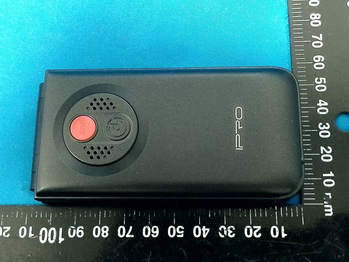
PQ4IPROV20S
Feb 11, 2026Mobile Phone
Equipment Class
DSS - Part 15 Spread Spectrum Transmitter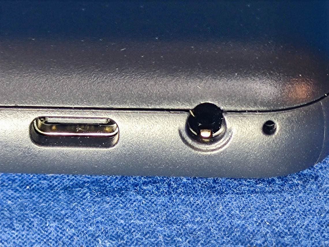
PQ4IPROK3
Jun 16, 2024Mobile Phone
Equipment Class
PCE - PCS Licensed Transmitter held to ear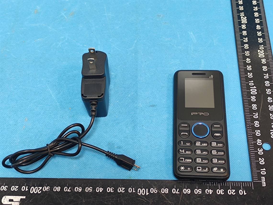
PQ4IPROK5
Jul 23, 2023Mobile Phone
Equipment Class
JBP - Part 15 Class B Computing Device Peripheral
PQ4IPROY300
Apr 13, 2023Smart Phone
Equipment Class
DSS - Part 15 Spread Spectrum Transmitter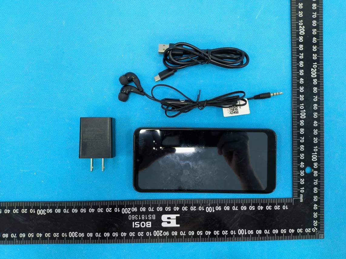
PQ4IPROS300
Nov 06, 2022Smart Phone
Equipment Class
PCE - PCS Licensed Transmitter held to ear