PQN44425RX2G4HAWK EYE BLUE SKY
Spin Master Toys Far East Ltd.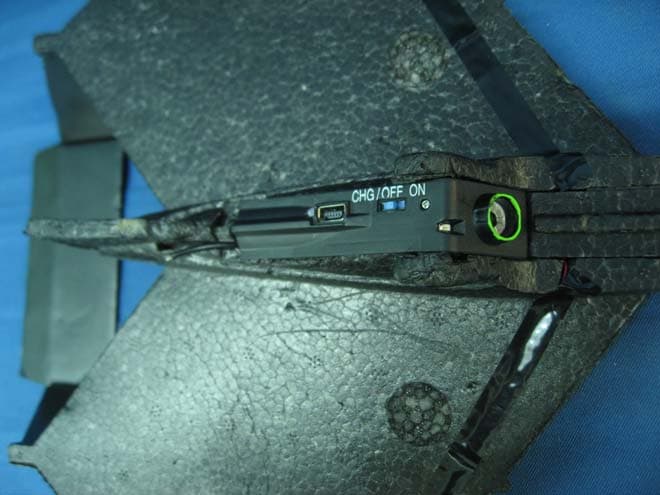
Click to zoom
Application Details
- Equipment Class
- DXX - Part 15 Low Power Communication Device Transmitter
- Date of Grant
- Aug 01, 2011
- Application Purpose
- Original Equipment
- Date of Application
- Aug 01, 2011
- Equipment Note
- HAWK EYE BLUE SKY
- Frequency Range
- 2401.00000000 - 2465.00000000
- Country
- Hong Kong
Documents & Files
Document Text
Text extracted from the exhibit documents filed with the FCC. Open a document above to read the original.
Users Manual
TM ® TM 1 23 CONTENTS LIST AND PARTS IDENTIFICATION BECOMING FAMILIAR WITH YOUR CONTROLLER/CHARGER CONTROLLER/CHARGER Function Indicator Direction Stick (LEFT/RIGHT) Signal Emitter Power Indicator Tail Wing Propeller Camera USB Port USB female socket Power Switch (ON/OFF/CHG) Propeller Main Wing Trimmer Knob USB Cable Storage Power Switch (ON/OFF/CHG) Throttle stick (UP/DOWN) INSTRUCTION GUIDE Instruction GuideCustom USB Cable2 Spare Propellers HAWK EYE™ BLUE SKY™ DANGER! NEVER INSERT ANY SHARP OBJECTS, PINS OR SCREWS INTO THE PLANE AS THIS MAY PUNCTURE THE INTERNAL BATTERY! Hawk Eye™ Blue Sky™ Controller HOW TO INSTALL YOUR BATTERIES TAKING VIDEOS OR PICTURES 1. Open the battery door with a screwdriver (pic.1). 2. If used batteries are present, remove these batteries from the unit by pulling up on one end of each battery. 3. Install new batteries as shown in the polarity diagram (+/-) inside the battery compartment (pic.2). 4. Replace battery door securely (pic.3). • Turn on your Hawk Eye™ Blue Sky™ plane and wait for a successful pairing. The red indicator will flash to show it’s searching for the controller. Turn on your controller and wait for a successful pairing. The green indicator will flash to show it’s searching for the plane. After a successful pairing, the green indicator on the controller will turn solid green and the red indicator on the plane will turn solid red. You are now able to take videos or photos, whether you’re on the ground or in the air. • To take a picture, press the picture button (right) (pic.1). The Hawk Eye™ Blue Sky™ will automatically adjust focus, ISO setting and shutter speed to take your image. This takes about 1.5 seconds, during which time the red indicator will light up on the controller (pic 2). Release the picture button and the red indicator turns off, now you are ready to take your next picture. NOTE: If the picture button is pressed while a video is recording, the video is stopped and a picture is taken. You can start the video recording again by pressing the video button. • To take videos, press the video button (left) once (pic.3). The red indicator on controller will turn solid red indicating that video is recording (pic.2). To stop video recording, press the video button again. The red indicator on controller will turn off. NOTE: Do not turn off the plane while the red light is on for video recording or else the video cannot be saved. • For best picture quality try to keep the plane flying straight and steady. • Video quality is also best during straight flight. Keep turns to a minimum. • Please respect the privacy of others. Refrain from taking videos and/or photos of other people without proper consent. • DO NOT fly too close to any obstacles or buildings for taking videos or pictures. Obstacles nearby may affect the airflow and the control of the plane. DO NOT fly the plane farther than 100 ft when taking videos. The plane will be out of range and drop off too far. It may be difficult to find. The green indicator on controller will be flashing when the plane is too far away. Please keep an eye on the indicator during flight, and move forward to fly it back when you see it flashing. pic.1 pic.3 INDICATION LIGHTS For further questions and problems, please visit our website www.airhogs.com. Battery requirement for Controller: Power Supply : Rating : DC 9 V, 0.45 W Requires 6 x 1.5 V AA size batteries (not included) BATTERY SAFETY INFORMATION: - Requires 6 x 1.5 V AA alkaline batteries (not included). - Batteries are small objects. - Replacement of batteries must be done by adults. - Follow the polarity (+/-) diagram in the battery compartment. - Promptly remove dead batteries from the toy. - Dispose of used batteries properly. - Remove batteries for prolonged storage - Only batteries of the same or equivalent type as recommended are to be used. - DO NOT incinerate used batteries. - DO NOT dispose of batteries in fire, as batteries may explode or leak. - DO NOT mix old and new batteries or types of batteries (i.e. alkaline/standard). - DO NOT use rechargeable batteries. - DO NOT recharge non-rechargeable batteries. - DO NOT short-circuit the supply terminals. Care and Maintenance: - Always remove batteries from the toy when it is not being used for a long period of time (controller only). - Wipe the toy gently with a clean damp cloth. - Keep the toy away from direct heat. - Do not submerge the toy in water. This can damage the electronic assemblies. - Always keep plane and controller in a box away from dirt and humidity when not being used. Special Note to Adults: - Regularly examine for damage to the plug, enclosure and other parts. In the event of any damage, the toy must not be used with the controller until the damage has been repaired. - This toy is not intended for children under 3 years old. - This toy must only be used with the recommended controller. - Do not try to charge other batteries with the controller. This device complies with Part 15 of the FCC rules. Operation is subject to the following two conditions: (1) This device may not cause harmful interference, and (2) This device must accept any interference received, including interference that may cause undesirable operation. This equipment has been tested and found to comply with the limits for Class B digital devices pursuant to Part 15 of the FCC rules. These limits are designed to provide reasonable protection against harmful interference to radio communications. This equipment generates, uses and can radiate radio frequency energy and, if not installed and used in accordance with the instruction, may cause harmful interference to radio communication. However, there is no guarantee that interference will not occur in a particular installation. If this toy does cause interference to radio or television reception (you can check this by turning the toy off and on while listening for the interference), one or more of the following measures may be useful: • Reorient or relocate…
Text truncated - open the document above for the full version.
Block Diagram
Antenna 2401 - 2465 MHz VGA CMOS (U7) camera circuit (U1,U2) Motor Circuit (U9,U10) MCU (U1) 27MHz Clock Frequency(X1) charging circuit (U5) Voltage Regulator (U2,U3,U4) 16MHz Clock Frequency(Y1) 2.4GHz RF Module (CWDP105-GO) S DRAM and Flash(U6)
External Photos
INTERTEK TESTING SERVICE Report No.: HK11060687-1 FCC ID: PQN44425RX2G4 Equipment Photographs Model: 44425RX (External) INTERTEK TESTING SERVICE Report No.: HK11060687-1 FCC ID: PQN44425RX2G4 Equipment Photographs Model: 44425RX (External)
ID Label/Location Info
The artwork of Label 1 Location of Label 1 Location of Label 2 The artwork of Label 2
Internal Photos
INTERTEK TESTING SERVICE Report No.: HK11060687-1 FCC ID: PQN44425RX2G4 Equipment Photographs Model: 44425RX (Internal) INTERTEK TESTING SERVICE Report No.: HK11060687-1 FCC ID: PQN44425RX2G4 Equipment Photographs Model: 44425RX (Internal) INTERTEK TESTING SERVICE Report No.: HK11060687-1 FCC ID: PQN44425RX2G4 Equipment Photographs Model: 44425RX (Internal) INTERTEK TESTING SERVICE Report No.: HK11060687-1 FCC ID: PQN44425RX2G4 Equipment Photographs Model: 44425RX (Internal) INTERTEK TESTING SERVICE Report No.: HK11060687-1 FCC ID: PQN44425RX2G4 Equipment Photographs Model: 44425RX (Internal)
Operational Description
Technical Description: The brief circuit description is listed as follows: - U1 and associated circuit act as MCU. - U2, U3, U4 and associated circuit act as Voltage Regulator. - U5 and associated circuit act as Charging Circuit. - U6 and associated circuit act as S DRAM and Flash. - U7 and associated circuit act as VGA CMOS. - U8 and associated circuit act as 2.4GHz RF Module. - U9, U10 and associated circuit act as Motor Circuit. - U1, U2 and associated circuit (external PCB) act as Camera Circuit. - X1 and associated circuit act as the clock frequency of U1. - Y1 and associated circuit act as the clock frequency of RF Module. Antenna Used: Internal, Integral antenna is used. Electrical specification Item Specification Remark Supply voltage 2.5V~3.6V Current consumption 1uA (typical) @Sleep mode 0.3mA (typical) @Idle mode 1.7mA (typical) @Stand-by mode 9mA (typical) @PLL Mode 16mA (typical) @Rx mode 20mA (typical) @Tx mode (Pout = 0dBm) Frequency 2400 – 2483 MHz ISM band Transmit output power 0 dBm @ room temperature typical Rx sensitivity -105 dBm (typical) @ 10Kbps mode, Dev = 40 KHz -100 dBm (typical) @ 250Kbps mode, Dev = 93 KHz -96 dBm (typical) @ 500Kbps mode, Dev = 186 KHz BER≦1E-3 Modulation FSK or GFSK Transmission distance 50meter BER≦1E-3 Interface 8 pin (2 x 4) header, Pitch: 2.54m/m Dimension 20mm(L) x 14.5mm(W) x 5mm(H) Not include the connector Operating temperature -40 ~ 85 °C Application: CWDP105-GO 2.4GHz Transceiver The CWDP105-GO module is designed for 2.4GHz ISM band wireless applications using AMICCOM A7105 (FSK or GFSK) transceiver. This module features a fully programmable frequency synthesizer by SPI. The maximum data rate is 500Kbps. Telemetry, Wireless Toys, Remote Control, Wireless Speaker, Wireless Earphone, Walkie-Talkie, Wireless House, Keyboard. Interface Pin No. Symbol Function Description Remark 1 GND Ground 2 VIN RF Module Supply Voltage Input 1.9V ~ 3.6V 3 NC No Connection 4 SCS SPI Chip Seiection 5 SCK SPI Clock 6 SDIO SPI Data I/O 7 GIO1 General Purpose I/O 1 8 GIO2 General Purpose I/O 2 Module Dimension Drawing (Top view)
Operational Description
A7105 Preliminary 2.4G FSK/GFSK Transceiver Jan. 2009, Version 0.3 (PRELIMINARY) 1AMIC Communication Corporation Document Title A7105 Data Sheet, 2.4GHz FSK/GFSK Transceiver with 500Kbps data rate Revision History Rev. No.HistoryIssue DateRemark 0.0Initial issue.Dec 27 th , 2007Preliminary 0.1Modified specification and add section for TX power settingFeb 20 th , 2008Preliminary 0.2Add top marking info., reflow profile, Carry tape & reel dimensions Oct. 9 th , 2008Preliminary 0.3Modify description of state machine and FIFO mode Rename IRQS1/IRQS2 to GIO1S/GIO2S Rename GPIO1/GPIO2 to GIO1/GIO2 Add Easy FIFO mode, Segment FIFO mode Delete thermal sensor function / external voltage measurement Delete TWWS function Add State diagram of quick/normal/power saving FIFO mode Add State diagram of Direct mode Rename Master Clock F CSCK to F MCLK Modify data rate support from 1K~500K to 2K ~ 500K Jan. 7 th , 2009Preliminary Important Notice: AMICCOM reserves the right to make changes to its products or to discontinue any integrated circuit product or service without notice. AMICCOM integrated circuit products are not designed, intended, authorized, or warranted to be suitable for use in life-support applications, devices or systems or other critical applications. Use of AMICCOM products in such applications is understood to be fully at the risk of the customer. A7105 Preliminary 2.4G FSK/GFSK Transceiver Jan. 2009, Version 0.3 (PRELIMINARY) 2AMIC Communication Corporation Table of Contents 1. General Description....................................................................................................................................................... 5 2. Typical Applications ....................................................................................................................................................... 5 3. Feature ......................................................................................................................................................................... 5 4. Pin Configurations ......................................................................................................................................................... 6 5. Pin Description (I: input; O: output, I/O: input or output)................................................................................................... 6 6. Chip Block Diagram....................................................................................................................................................... 7 7. Absolute Maximum Ratings............................................................................................................................................ 8 8. Electrical Specification................................................................................................................................................... 8 9. Control Register ...........................................................................................................................................................10 9.1 Control register table............................................................................................................................................10 9.2 Control register description ..................................................................................................................................12 9.2.1 Mode Register (Address: 00h)..................................................................................................................12 9.2.2 Mode Control Register (Address: 01h)......................................................................................................12 9.2.3 Calibration Control Register (Address: 02h)..............................................................................................13 9.2.4 FIFO Register I (Address: 03h).................................................................................................................13 9.2.5 FIFO Register II (Address: 04h)................................................................................................................13 9.2.6 FIFO DATA Register (Address: 05h) .........................................................................................................13 9.2.7 ID DATA Register (Address: 06h)................................................................................................................14 9.2.8 RC OSC Register I (Address: 07h) .............................................................................................................14 9.2.9 RC OSC Register II (Address: 08h).............................................................................................................14 9.2.10 RC OSC Register III (Address: 09h)..........................................................................................................14 9.2.11 CKO Pin Control Register (Address: 0Ah) .................................................................................................14 9.2.12 GIO1 Pin Control Register I (Address: 0Bh)...............................................................................................15 9.2.13 GIO2 Pin Control Register II (Address: 0Ch) .............................................................................................15 9.2.14 Clock Register (Address: 0Dh)..................................................................................................................16 9.2.15 Data Rate Register (Address: 0Eh) ...........................................................................................................17 9.2.16 PLL Register I (Address: 0Fh)...................................................................................................................17 9.2.17 PLL Register II (Address: 10h)..................................................................................................................17 9.2.18 PLL Register III (Addre…
Text truncated - open the document above for the full version.
Schematics
11 A A Decoupling capacitor for U1 Decoupling capacitor for U1 J2 J3 1 1 1 10 00 0 LEFT PWM RIGHT PWM 6% 6% 9% 9% 12% 12% 3% 3% RS232 DEBUG PORT SPI DEBUG PORT MAR97327AH B 1 5 Friday, July 15, 2011 Title Size Document Number Rev Date: Sheet of V_A[0..10] V_D[0..15] USB_DN USB_DP USB_DET X27M_IN X27M_OUT RST N_RE N_D[0..7] N_ALE N_WE N_RDY N_CLE N_CE S_SDA S_SCL LO_DET USB_MODE DGNDVCC_2V5 VCC_3V VCC_2V5 S_SCL S_SDA DGND DGND DGND S_IMG4 S_IMG5 S_IMG7 S_IMG6 S_IMG8 DGND DGND S_IMG9 DGNDVCC_2V5 DGND VCC_3V DGND USB_MODE DGND V_BS0 V_A10 VCC_3V VCC_3V V_A0 V_RAS V_CAS V_CS V_WE X27M_IN DGND V_A5 VCC_2V5 V_A4 X27M_OUT V_A6 V_A8 VCC_2V5 DGND DGND V_A7 VCC_2V5 V_A2 V_A9 V_A3 DGND V_A1 VCC_2V5 V_D1 V_D3 V_D2 DGND V_D5 VCC_2V5 V_D4 V_D0 DGND VCC_3V VCC_3V DGND V_D6 V_D7 S_IMG3 V_D8 SPI_SCS DGND S_IMG2 S_PCLK V_D9 SPI_CLK LO_DET S_VSYNC USB_DET DGND S_HSYNC S_MCLK V_D13 V_D10 V_D11 V_D12 VCC_3V DGND DGNDV_CKEDGND V_D15 V_D14 DGND VCC_2V5 DGNDVCC_2V5 VCC_2V5 VCC_3V VCC_3V V_LDQM V_UDQM DGND VCC_3V RST USB_DN USB_DP DGND DGND VCC_3V VCC_3V DGND DGND DGND VCC_2V5 VCC_2V5 VCC_2V5 DGNDVCC_3V N_ALE N_CE N_RDY N_CLE N_D7 N_D6 N_D5 N_D4 N_D3 N_D2 V_CLK N_D1 N_D0 N_RE N_WE J2 LEFT MOTOR SPI_SDC J2J3 J3 LEFT MOTOR RIGHT MOTOR ID LEFT MOTOR PROTECT RIGHT MOTOR PROTECT RIGHT MOTOR PROTECT LEFT MOTOR PROTECT TXD0 RF_GPO1 RF_SCS RIGHT MOTOR TXD0 SPI_SCS SPI_DI SPI_CLK SPI_DO RF_SCS RF_GPO1 SPI_DO CHARGE STAUS CHARGE ON/OFF CHARGE LED CHARGE ON/OFF CHARGE STAUS VCC_3V S_MCLK S_IMG7 S_IMG2 S_IMG3 S_IMG6 S_IMG4 S_IMG5 CHARGE LED SPI_DI ID SPI_DCS SPI_DO SPI_CLK S_VSYNC S_SDA S_IMG9 S_HSYNC S_IMG8 S_SCL S_PCLK USB_DN 2 USB_DP 2 USB_DET 2 LO_DET 2 LEFT MOTORRIGHT MOTORRIGHT MOTOR PROTECTLEFT MOTOR PROTECT CHARGE ON/OFFCHARGE STAUS VCC_2V5 DGND DGND VCC_3V DGND VCC_3V DGND VCC_3V DGND VCC_3V VCC_2V5 DGND VCC_3V DGND VCC_3V DGND VCC_3V DGND DGND DGNDVCC_3V VCC_3V TP12 MR97327AH MARS U1 MR97327AH 2356789 1011121314151617181920212223242526272829303132333435363738394041424344 14 4546 47 48 49 50 51 52 53 54 55 56 57 58 59 60 61 62 63 64 65 66 67 68 69 70 71 72 73 74 75 76 77 78 79 80 81 82 83 84 85 86 87 88 89 90 91 92 93 138137136135134133132131130129128127126125124123122121120119118117116115114113112111110109108107106105104103102101100999897969594 184 183 182 181 180 179 178 177 176 175 174 173 172 171 170 169 168 167 166 165 164 163 162 161 160 159 158 157 156 155 154 153 152 151 150 149 148 147 146 145 144 143 142 141 140 139 0 GND GND IMG2/GPIO9[0]PCLK HSYNC VSYNC MCLK SCL SDA NROMCE/GPIO6[4] ROMA15/GPIO6[2] ROMA14/GPIO6[1] VCC2.5V ROMA13/GPIO6[0] ROMA12/GPIO4[6] ROMA11/GPIO4[5] ROMA[10]/GPIO4[4]/NAND_RDY ROMA[9]/GPIO4[3]/NAND_CE VCC3VVCC3VROMA[8]/GPIO4[2]/NAND_ALE V_LDQM ROMA7/GPIO4[1] ROMA[6]/GPIO4[0]/NAND_CLE PANEL_D7/RFI_TX_IN/GPIO8[7] PANEL_D6/RFI_DATA/GPIO8[6] PANEL_D5/GPIO8[5]/CPU_TXD0 PANEL_D4/GPIO8[4]/CPU_RXD0 PANEL_D3/GPIO8[3] PANEL_D2/GPIO8[2] PANEL_D1/GPIO8[1] PANEL_D0/GPIO8[0] VCC2.5V R2.5V R2.5V R3.3V R3.3V GND GND GND GND GND GND IMG3/GPIO9[1] PANEL_CLK PANEL_VSYNC PANEL_HSYNC PANEL_FRAME/I2S_DCLK V_WE V_CAS V_RAS V_CS V_BS0 V_A10 V_A0 V_A1 V_A2 V_A3 VCC3V VCC3V GND VCC2.5V V_A4 V_A5 V_A6 V_A7 V_A8 V_A9 PLL_2.5V PLL_GND GND GND X27MIN X27MOUT VCC2.5V VCC2.5V RTCV33 PWR_KEEP RST X_GND X_GND RTC25V RTC25V RTC25V X32KIN X32KOUT X_GND X_GND GND_USB DN DP 3.3V USB 3.3V ROMA16/GPIO6[3] NEA SWD USB_MODE POWER-KEY GPIO2[0]/I2S_SDO/A_PWM GPIO2GPIO2[1]/I2S_SDI GPIO2[2]/I2S_BCLK GPIO0[3] GPIO0[4]/I2S_DCLK GPIO0[5]/I2S_ACLK ROMA0/GPIO3[0]/I2S_DCLK ROMA1/GPIO3[1]/I2S_ACLK ROMA2/GPIO3[2] ROMA3/GPIO3[3]/PWM_OUT ROMA4/GPIO3[4]/NAND_NWE ROMA5/GPIO3[5]/NAND_NRE V_CLK V_A11 V_A12 VCC2.5V VCC2.5V VCC3VVCC3V V_UDQM TEST ROMD2/GPIO5[2]/NAND_D2 ROMD3/GPIO5[3]/NAND_D3 GND GND GND GND V_CKE ROMD[4]/GPIO5[4]/NAND_D4 ROMD[5]/GPIO5[5]/NAND_D5 ROMD[6]/GPIO5[6]/NAND_D6 ROMD[7]/GPIO5[7]/NAND_D7 GPIO1[0]/SPI_SDI GPIO1[1]/SPI_SDO GPIO1[2]/SPI_CLK GPIO1[3]/SPI_NCS GPIO0[0] GPIO0[1] GPIO0[2] USB_DET IMG4/GPIO9[2] IMG5/GPIO9[3] IMG6/GPIO9[4]/CPU_RXD0 IMG7/GPIO9[5]/CPU_TXD0 IMG8/RFI_RX_D/GPIO9[6] IMG9/RFI_TX_D/GPIO9[7] SD_D0/GPIO7[0] SD_D1/GPIO7[1] SD_D2/GPIO7[2] SD_D3/GPIO7[3] SD_CMD/GPIO7[4] GND SD_CLK VCC3V NROMRD/GPIO6[5] NROMWR/GPIO6[6] VCC2.5V V_D0 V_D1 GND V_D2 V_D3 V_D4 V_D5 GND V_D6 V_D7 GND V_D8 V_D9 GND GND V_D10 V_D11 VCC3V V_D12 V_D13 GND V_D14 V_D15 ROMD0/GPIO5[0]/NAND_D0 ROMD1/GPIO5[1]/NAND_D1 VCC2.5V VCC2.5V VCC3V V_BS1 PAD CB1 0.1uF R12 10K R7 300K C1 10uF 12 TP6 1 TP13 R4 1.5K X1 27MHz Y-2X6-Z TP5 1 TP8 1 R847K CB5 0.1uF R1 1K CB3 0.1uF TP9 1 CB4 0.1uF TP7 1 C2 10uF 12 R647K TP1 1 SW1 R3 1.5K CB2 0.1uF TP2 1 CB6 0.1uF TP11 TP3 1 J1CON9 123456789 R9 10K C510uF 12 C4 10pF TP10 R10 NC R510K C610uF 12 TP4 1 R11 NC C7 10pF J2CON9 123456789 C3 0.1uF K1 12 V_A[0..10] 3 V_D[0..15] 3 N_RE N_CLE N_ALE N_D[0..7] 3 N_WE N_RDY N_CE V_CKE V_UDQM V_LDQM V_WEV_RASV_CASV_CSV_BS0 V_CLK SPI_DCS SPI_SCSSPI_DISPI_CLKSPI_DORF_SCS RF_GPO1 55 44 33 22 11 D D C C B B A A Mars Semiconductor Corporation SW MIDDLE :OFF SW DOWN(RIGHT) WORK MODE SW UP(LEFT):USB AND CHARGE MODE FOR FCC FOR FCC FOR FCC FOR FCC for protect the PC usb HUB POWER B 2 5 Friday, July 15, 2011 Title Size Document Number Rev Date: Sheet of LO_DET CHARGE STAUS USB_DP CHARGE ON/OFF USB_DN CHARGE STAUS CHARGE ON/OFF CHARGE STAUS LO_DET USB_DN 1 USB_DP 1 CHARGE ON/OFF USB_DET 1 DGND VUSB_OUT BAT_CHG DGND VCC_3V DGND VUSB VCC_3V BAT_CHG VUSB VUSB_OUT BAT_PWR VUSB_OUT PWR_IN DGND DGND BAT_PWR DGND DGND DGND DGND DGND DGNDVCC_3V VCC_3V DGND DGND DGND DGND DGNDDGND C14 22uF 104 C9 C11 104 D1 1N5819 R17 100K R22 100K R14 10K 47P C51 J3USB 123456 VBUS D-D+GND GND GND L2 601 41 23 R13 10K D4 1N4001 C8 100UF R15 10K U4AIC1680-3.0 2 1 3 GND VOUT VDD R21 27R R25 10K C12 1NF U2LC1206-3.3V 3 1 2 IN GND OUT FU1 CB0603-1000T R24 100R L1 27uH 104 C50 1uF C15 U3 BL8530C 123 45 CEOUT NC GND EXT R51 15K U5 LC6000 1 2 3 45 CHRG GND BAT VCC PROG SW2 SW ROTARY 2P-3W 865421 73 D3 1N5819 Q2SI2302 R16 1.5K R19 NC C13 22uF BAT1 BAT_JACK 12 12 R18 1.5K R20 27R 47P C52 104 C53 C10 10uF R26 22K R23 2.7K D…
Text truncated - open the document above for the full version.
Test Report
INTERTEK TESTING SERVICES Report No.: HK11060687-1 Sample No.: 1/1 Code: FCC15C_d / Effective Date: 26 Jan 2010 ( of ) Average Factor Plot – Pursuant to FCC Part 15 Section 15.249 Requirement INTERTEK TESTING SERVICES Report No.: HK11060687-1 Sample No.: 1/1 Code: FCC15C_d / Effective Date: 26 Jan 2010 ( of ) Average Factor Plot – Pursuant to FCC Part 15 Section 15.249 Requirement INTERTEK TESTING SERVICES Report No.: HK11060687-1 Sample No.: 1/1 Code: FCC15C_d / Effective Date: 26 Jan 2010 ( of ) Average Factor Plot – Pursuant to FCC Part 15 Section 15.249 Requirement INTERTEK TESTING SERVICES Report No.: HK11060687-1 Sample No.: 1/1 Code: FCC15C_d / Effective Date: 26 Jan 2010 ( of ) Average Factor Plot – Pursuant to FCC Part 15 Section 15.249 Requirement
Test Report
INTERTEK TESTING SERVICES Report No.: HK11060687-1 Sample No.: 1/1 Code: FCC15C_d / Effective Date: 26 Jan 2010 ( of ) Bandedge Plot – Pursuant to FCC Part 15 Section 15.249 Requirement
Test Report
- The test report only allows to be revised within the retention period unless further standard or the requirement was noticed. - This report is for the exclusive use of Intertek's Client and is provided pursuant to the agreement between Intertek and its Client. Intertek's responsibility and liability are limited to the terms and conditions of the agreement. Intertek assumes no liability to any party, other than to the Client in accordance with the agreement, for any loss, expense or damage occasioned by the use of this report. Only the Client is authorized to permit copying or distribution of this report and then only in its entirety. Any use of the Intertek name or one of its marks for the sale or advertisement of the tested material, product or service must first be approved in writing by Intertek. The observations and test results in this report are relevant only to the sample tested. This report by itself does not imply that the material, product, or service is or has ever been under an Intertek certification program. Intertek Testing Services Hong Kong Ltd. 2/F., Garment Centre, 576 Castle Peak Road, Kowloon, Hong Kong. Tel: (852) 2173 8888 Fax: (852) 2785 5487 Website: www.hk.intertek-etlsemko.com TEST REPORT Report No.: HK11060687-1 Spin Master Toys Far East Limited Application For Certification (Original Grant) (FCC ID: PQN44425RX2G4) Transceiver Prepared and Checked by: Approved by: Signed On File Kung Wing Cheong, Steven Engineer Chan Chi Hung, Terry Assistant Supervisor Date: August 01, 2011 INTERTEK TESTING SERVICES Report No.: HK11060687-1 FCC ID: PQN44425RX2G4 i GENERAL INFORMATION Spin Master Toys Far East Limited MODEL: 44425RX FCC ID: PQN44425RX2G4 Grantee: Spin Master Toys Far East Limited Grantee Address: Room 1113A, 11/F., Chinachem Golden Plaza, 77 Mody Road, Tsim Sha Tsui East, Kowloon, Hong Kong Contact Person: Hanson Zhou Tel: 86769-81080068 Fax: N/A e-mail: [email protected] Manufacturer: Spin Master Toys Manufacturer Address: Room 1113A, 11/F., Chinachem Golden Plaza, 77 Mody Road, Tsim Sha Tsui East, Kowloon, Hong Kong Brand Name: Spin Master Ltd. Model: 44425RX Additional Model: 1021705, 1021706, 1022264, 1022495, 1021816, 6017072, 6017073, 6017106 Type of EUT: Transceiver Description of EUT: HAWK EYE BLUE SKY Serial Number: N/A FCC ID : PQN44425RX2G4 Date of Sample Submitted: June 13, 2011 Date of Test: June 23, 2011 Report No.: HK11060687-1 Report Date: August 01, 2011 Environmental Conditions: Temperature: +10 to 40°C Humidity: 10 to 90% INTERTEK TESTING SERVICES Report No.: HK11060687-1 FCC ID: PQN44425RX2G4 ii SUMMARY OF TEST RESULT SPIN MASTER TOYS FAR EAST LIMITED MODEL: 44425RX FCC ID: PQN44425RX2G4 TEST SPECIFICATION REFERENCE RESULTS Maximum Peak Output Power 15.247(b), (c) / RSS-210 A8.4 N/A Hopping Channel Carrier Frequencies Separation 15.247(e) / RSS-210 A8.1 (for 2.4GHz Digital) N/A 20dB Bandwidth of the Hopping Channel 15.247(a) / RSS-210 A8.1 N/A Number of Hopping Frequencies 15.247(e) / RSS-210 A8.1 N/A Average Time of Occupancy of Hopping Frequency 15.247(e) / RSS-210 A8.1 N/A Antenna Conducted Spurious Emissions 15.247(d) / RSS-210 A8.5 N/A Radiated Spurious Emissions 15.247(d) / RSS-210 A8.5 N/A RF Exposure Compliance 15.247(i) / RSS-Gen 5.5 N/A Transmitter Power Line Conducted Emissions 15.207 / RSS-Gen 7.2.2 N/A Transmitter Field Strength (for 27MHz) 15.227 / RSS-310 3.8 N/A Transmitter Field Strength (for 40MHz) 15.229 / RSS-210 A2.7 N/A Transmitter Field Strength, Bandwidth and Timing Requirement 15.231(a) / RSS-210 A1.1.1 (for Remote Control) N/A Transmitter Field Strength, Bandwidth and Timing Requirement 15.231(e) / RSS-210 A1.1.5 (for 433MHz) N/A Transmitter Field Strength and Bandwidth Requirement 15.239 / RSS-210 A2.8 (for 88-108MHz) N/A Transmitter Field Strength and Bandwidth Requirement 15.249 / RSS-210 A2.9 (for 902-928MHz or 2.4GHz) Pass Transmitter Field Strength and Bandwidth Requirement 15.235 / RSS-310 3.9 (for 49MHz) N/A Receiver / Digital Device Radiated Emissions 15.109 / ICES-003 N/A Digital Device Conducted Emissions 15.107 / ICES-003 N/A Note: 1. The EUT uses a permanently attached antenna which, in accordance to section 15.203, is considered sufficient to comply with the pervisions of this section. 2. Pursuant to FCC part 15 Section 15.215(c), the 20 dB bandwidth of the emission was contained within the frequency band designated (mentioned as above) which the EUT operated. The effects, if any, from frequency sweeping, frequency hopping, other modulation techniques and frequency stability over excepted variations in temperature and supply voltage were considered. INTERTEK TESTING SERVICES Report No.: HK11060687-1 FCC ID: PQN44425RX2G4 iii Table of Contents 1.0 General Description....................................................................................... 1 1.1 Product Description ...................................................................................... 1 1.2 Related Submittal(s) Grants .......................................................................... 1 1.3 Test Methodology ......................................................................................... 1 1.4 Test Facility .................................................................................................. 1 2.0 System Test Configuration ............................................................................ 2 2.1 Justification................................................................................................... 2 2.2 EUT Exercising Software .............................................................................. 2 2.3 Special Accessories...................................................................................... 2 2.4 Equipment Modification................................................................................. 2 2.5 Measurement Uncertainty ............................................................................. 2 2.6 Support Equipment List and Description.…
Text truncated - open the document above for the full version.
Test Setup Photos
INTERTEK TESTING SERVICE Report No: HK11060687-1 FCC ID: PQN44425RX2G4 Configuration Photographs Worst-Case Radiated Emissions (Front View) Model : 44425RX INTERTEK TESTING SERVICE Report No: HK11060687-1 FCC ID: PQN44425RX2G4 Configuration Photographs Worst-Case Radiated Emissions (Back View) Model : 44425RX
Contact Information
Applicant
Tommy So(Senior Quality Manager)
Technical Contact
Intertek Testing Services Hong Kong LtdTerry Chan
[email protected]21738503
2/F Garment Centre · Kowloon · Hong Kong
Non-Technical Contact
Intertek Testing Services Hong Kong LtdTerry Chan
[email protected]21738503
Test Firm
Intertek Testing Services Hong Kong Ltd.Billy Chow
Technical Specifications
| # | Rule Parts | Frequency Range | Power Output |
|---|---|---|---|
| 1 | 15C | 2.40 GHz - 2.46 GHz | - |
Other Applications from Spin Master Toys Far East Ltd.
PQN66807TX2G4R1
Jul 03, 2024MJC RDC Megalodon Storm GEN 1pk SLD(MCU ABE2402X1)
Equipment Class
DXX - Part 15 Low Power Communication Device TransmitterPQN66807RX2G4R1
Jul 03, 2024MJC RDC Megalodon Storm GEN 1pk SLD(MCU ABE2402X1)
Equipment Class
DXX - Part 15 Low Power Communication Device Transmitter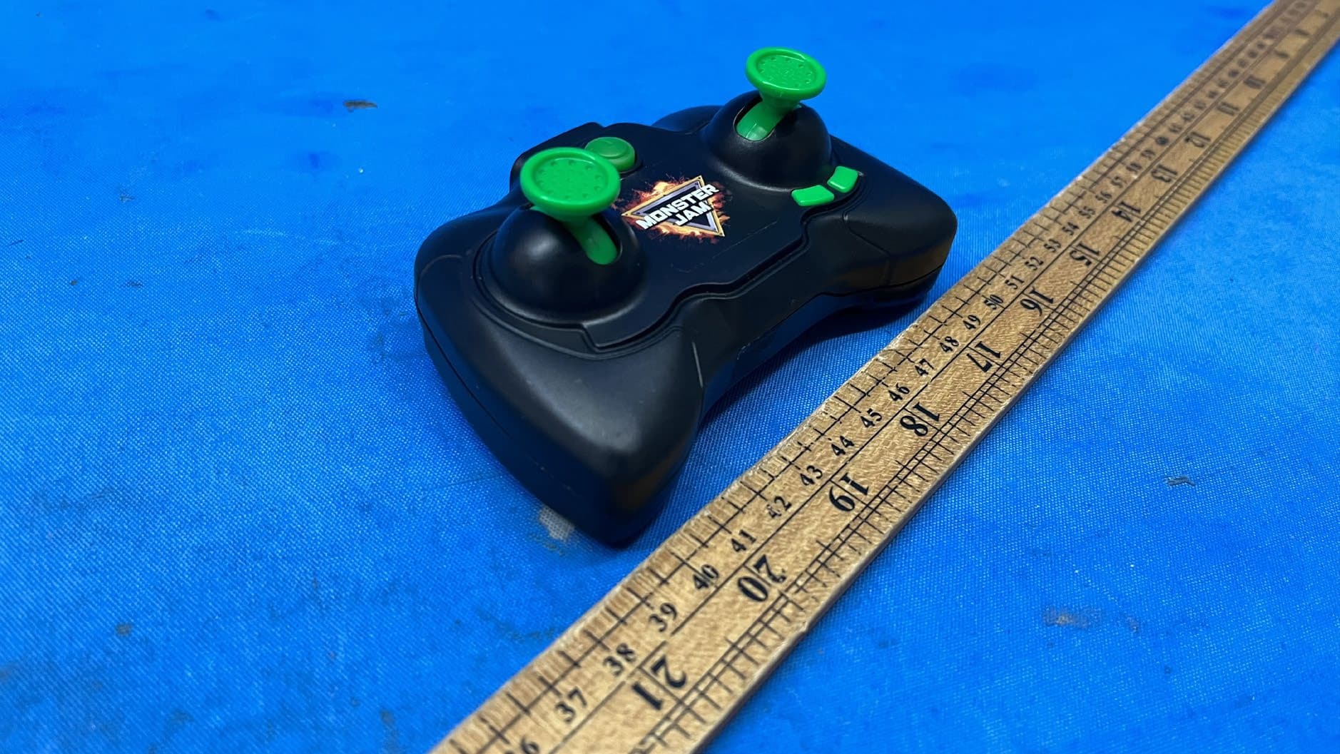
PQN66804TX2G43
Apr 03, 2024MJC Mega Grave Digger, MJC RDC Mega Grave Digger, MJC RDC Mega El Toro Loco, MNJ RDC Mega Megalodon RC, TRGT MIXED MEGA MJ HAFT PALLET, MJC COP Mega RC Asst PAL
Equipment Class
DXX - Part 15 Low Power Communication Device Transmitter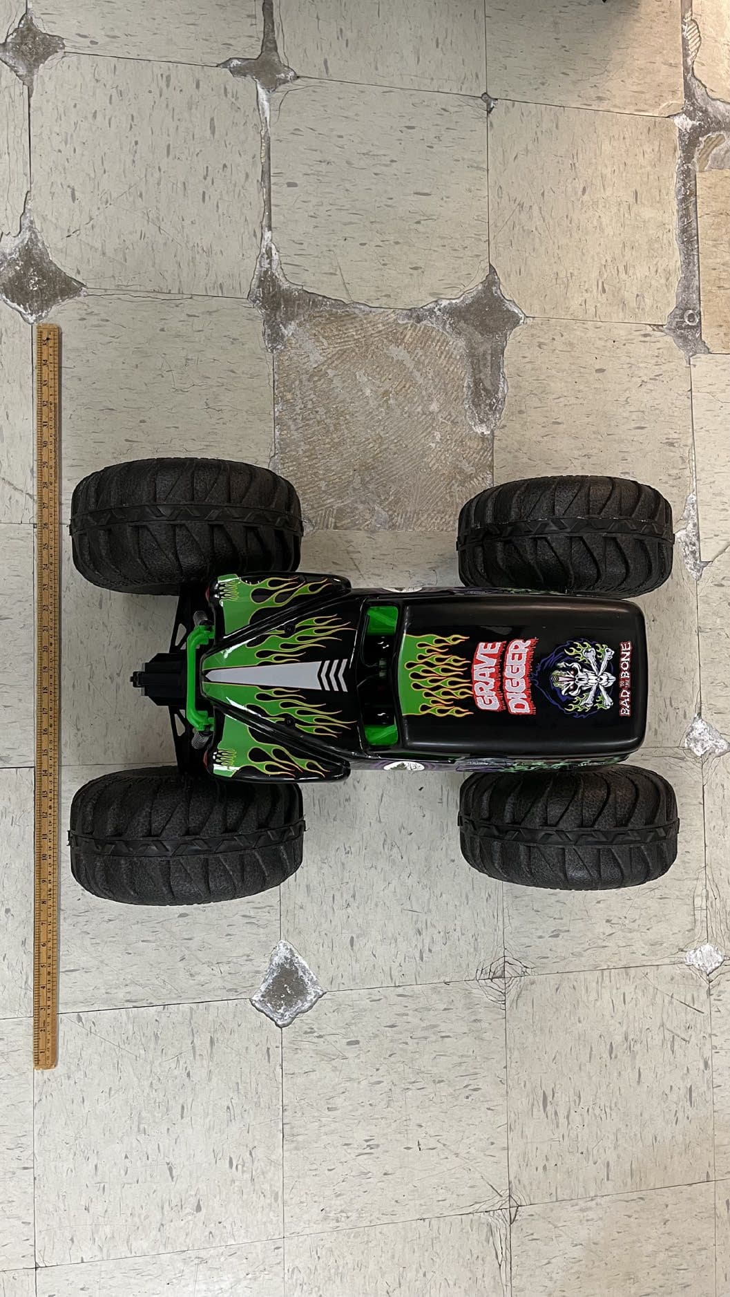
PQN66804RX2G43
Apr 03, 2024MJC Mega Grave Digger, MJC RDC Mega Grave Digger, MJC RDC Mega El Toro Loco, MNJ RDC Mega Megalodon RC, TRGT MIXED MEGA MJ HAFT PALLET, MJC COP Mega RC Asst PAL
Equipment Class
DXX - Part 15 Low Power Communication Device TransmitterPQN68126TX2G4
Aug 29, 2023HEX RDC HxmdPrSrEltStnrCrct EN GML2pkSLD
Equipment Class
DXX - Part 15 Low Power Communication Device Transmitter