PQN44438RX2G4ARH RDC Helix X4 Quad-Copter
Spin Master Toys Far East Ltd.
Click to zoom
Application Details
- Equipment Class
- DXX - Part 15 Low Power Communication Device Transmitter
- Date of Grant
- Apr 10, 2013
- Application Purpose
- Original Equipment
- Date of Application
- Apr 10, 2013
- Equipment Note
- ARH RDC Helix X4 Quad-Copter
- Frequency Range
- 2412.00000000 - 2469.00000000
- Country
- Hong Kong
Documents & Files
Document Text
Text extracted from the exhibit documents filed with the FCC. Open a document above to read the original.
Users Manual
Battery requirement for Helix X4™: / Caractéristiques de la batterie du Helix X4™ : / Especificaciones de la batería del Helix X4™: Power Supply: / Alimentation : / Alimentación: Rating: DC 3.7 V, 1.8 W / Puissance nominale : 3,7 V CC, 1,8 W / Potencia: 3,7 V, 1,8 W, CC Batteries: 1 x 3.7 V LiPo Rechargeable Battery Pack / Piles : 1 bloc-piles rechargeable LiPo de 3,7 V / Pilas: 1 paquete de pilas recargables de polímero de litio de 3,7 V Requires 1 x 3.7 V LiPo Rechargeable Battery Pack (included) / Requiert 1 bloc-piles rechargeable LiPo de 3,7 V (compris) / Requiere 1 paquete de pilas recargables de polímero de litio de 3,7 V (viene incluido) Battery requirement for Controller: / Caractéristiques de la batterie de la radiocommande : / Especificaciones de las baterías del controlador: Power Supply: / Alimentation : / Alimentación: Rating: DC 12 V, 0.45 W / Puissance nominale : 12 V CC, 0,45 W / Potencia: 12 V, 0,45 W, CC Batteries: 8 x 1.5 V AA/LR6/AM3 / Piles : 8 piles 1,5 V AA/LR6/AM3 / Batería: 8 pilas de formato AA/LR6/AM3 de 1,5 V Requires 8 x 1.5 V AA size batteries (not included) / Fonctionne avec 8 piles AA 1,5 V (non fournies) / Requiere 8 pilas de 1,5 V y formato AA (no incluidas) e FCC Statement: This device complies with Part 15 of the FCC rules. Operation is subject to the following two conditions: (1) This device may not cause harmful interference, and (2) This device must accept any interference received, including interference that may cause undesirable operation. This equipment has been tested and found to comply with the limits for Class B digital devices pursuant to Part 15 of the FCC rules. These limits are designed to provide reasonable protection against harmful interference to radio communications. This equipment generates, uses and can radiate radio frequency energy and, if not installed and used in accordance with the instruction, may cause harmful interference to radio communication. However, there is no guarantee that interference will not occur in a particular installation. If this toy does cause interference to radio or television reception (you can check this by turning the toy off and on while listening for the interference), one or more of the following measures may be useful: • Reorient or relocate the receiving antenna • Increase the separation between the toy and the radio or the TV • Consult the dealer or an experienced TV-radio technician for help. Shielded cables must be used with this unit to ensure compliance with the Class B FCC limits. NOTE: Changes, adjustments or modifications to this unit, including but not limited to, replacement of any transmitter component (crystal, semiconductor, etc.) could result in a violation of FCC rules under part 15 and/or 95 and must be expressly approved by Spin Master Ltd. or they could void the user’s authority to operate the equipment. f Déclaration de la FCC : Cet appareil est conforme à l’article 15 de la réglementation de la FCC. Son utilisation est soumise aux deux conditions suivantes : (1) cet appareil ne doit pas causer d’interférences nuisibles, et 2) cet appareil doit tolérer toutes les interférences reçues, y compris celles pouvant entraîner un fonctionnement indésirable. Cet équipement a été testé et jugé conforme aux limites de la classe B pour les équipements numériques en vertu de l’article 15 de la réglementation de la FCC. Ces limites ont été instaurées pour assurer une protection raisonnable contre toute interférence nuisible avec les communications radios. Cet équipement génère, utilise et peut émettre de l’énergie de fréquence radio. S’il n’est pas installé et utilisé selon le mode d’emploi, il peut causer des interférences nuisibles aux communications radios. Cependant, selon l’installation, des interférences peuvent être constatées. Si ce jouet cause des interférences à la réception radio ou télévisée (ce qui est vérifiable en l’éteignant, puis en le rallumant tout en écoutant s’il y a des interférences), suivre une ou plusieurs des recommandations suivantes : • Réorienter ou déplacer l’antenne réceptrice • Augmenter la distance entre le jouet et la radio ou la télévision • Consulter le revendeur ou demander l’aide d’un technicien radio/T.V. expérimenté. Pour respecter les limites de la classe B de la réglementation de la FCC, cet appareil doit être utilisé avec des câbles blindés. REMARQUE : tout changement, réglage ou modification de cet appareil, incluant mais ne se limitant pas au remplacement de tout composant du transmetteur (cristal, semi-conducteur, etc.), pourrait constituer une violation de l’article 15 et/ou 95 de la règlementation de la FCC, et doit être expressément approuvé par Spin Master Ltd., sous peine d’entraîner l’annulation du droit de l’utilisateur d’exploiter l’équipement. E Declaración de la FCC: Este aparato cumple con el artículo 15 de las normas de la FCC. El funcionamiento está sujeto a las dos siguientes condiciones: 1) Este aparato no debe causar interferencias perjudiciales, y 2) Este aparato debe aceptar cualquier interferencia recibida, incluidas las que podrían causar un funcionamiento no deseado. Este equipo se sometió a las pruebas debidas y se comprobó que cumple con los requisitos específicos para aparatos digitales de clase B en conformidad con el artículo 15 de las normas de la FCC. Estos requisitos están diseñados para proporcionar protección razonable contra interferencias perjudiciales en las comunicaciones por radio. Este juguete genera, utiliza y puede emitir energía de radiofrecuencia. Si no se instala y se utiliza de acuerdo con la guía de instrucciones, puede causar interferencias en las comunicaciones por radio. Sin embargo, en función de la instalación, pueden ocurrir interferencias. Si este juguete ocasiona interferencias perjudiciales en la recepción radio o televisiva (lo cual se puede comprobar encendiendo y apagando el juguete mientras se escucha la interferencia), seguir una o varias de las siguientes recomendaciones: • Volver a orie…
Text truncated - open the document above for the full version.
Block Diagram
Revision 1.1 13 of 191 nRF24LE1 Preliminary Product Specification 2.2 Block diagram Figure 1. nRF24LE1 block diagram To find more information on the blocks, see Table 1. below: Table 1. Block diagram cross references NameReference Memory (Program, Data, NVMEM)Chapter 5 on page 62 Power managementChapter 11 on page 102 RF TransceiverChapter 3 on page 16 2-WireChapter 20 on page 154 SPI (Master and Slave)Chapter 18 on page 142 GPIOChapter 17 on page 127 PWMChapter 23 on page 169 WatchdogChapter 10 on page 100 RF Transceiver SPI Master Program (FLASH) IRAM 256 byte Data (SRAM) VREG1V7 XOSC 16MHz Power Management Interrupt Control System Config SFR-bus RCOSC 16MHz Brown out detector RTC Watch dog POR OCI CPU Timers Serial ports R80515 MEM-bus VREG1V2 NVMEM (FLASH) Memory bus decoder VDD_1V7 VDD_1V2 Debounce Debounce mux CK16M XOSC 32kHz RCOSC 32 kHz Debounce Debounce mux CKLF SPI Slave 2-Wire M/S GPIO PWM Crypt CoProc L01 i/f (SPI) ADC ADC i/f Digital Crossbar Pin Crossbar 1.9 V - 3.6V Multi purpose pins - bidir dig/ analog Retention Latches WakeUP OnPin Wakeup Config RNG Comparator Revision 1.1 17 of 191 nRF24LE1 Preliminary Product Specification 3.2 Block diagram Figure 5. RF Transceiver block diagram 3.3 Functional description This section describes the different operating modes of the RF Transceiver and the parameters used to control it. The RF Transceiver module has a built-in state machine that controls the transitions between the different operating modes. The state machine is controlled by SFR register RFCON and RF transceiver register CONFIG, see section 3.5 for details. 3.3.1 Operational Modes You can configure the RF Transceiver to power down, standby, RX and TX mode. This section describes these modes in detail. 3.3.1.1 State diagram The state diagram (Figure 6.) shows the operating modes of the RF Transceiver and how they function. At the end of the reset sequence the RF Transceiver enters Power Down mode. When the RF Transceiver enters Power Down mode the MCU can still control the module through the SPI and the rfcsn bit in the RFCON register. There are three types of distinct states highlighted in the state diagram: •Recommended operating mode: is a recommended state used during normal operation. •Possible operating mode: is a possible operating state, but is not used during normal operation. •Transition state: is a time limited state used during start up of the oscillator and settling of the PLL. RF Receiver ANT1 ANT2 Enhanced ShockBurst Baseband Engine TX FIFOs RX FIFOs Radio Control GFSK Modulator SPI (Slave) PA LNA TX Filter RX Filter RF SynthesiserPower Management RF TransmitterBaseband RFIRQ GFSK Demodulator Register map RFCON.rfcken XOSC16M RFCON.rfce RFCON.rfcsn SPI (Master)
External Photos
INTERTEK TESTING SERVICE Report No.: HK13020722-3 FCC ID: PQN44438RX2G4 Equipment Photographs Model : 44438RX (External) INTERTEK TESTING SERVICE Report No.: HK13020722-3 FCC ID: PQN44438RX2G4 Equipment Photographs Model : 44438RX (External)
Internal Photos
INTERTEK TESTING SERVICE Report No.: HK13020722-3 FCC ID: PQN44438RX2G4 Equipment Photographs Model: 44438RX (Internal) INTERTEK TESTING SERVICE Report No.: HK13020722-3 FCC ID: PQN44438RX2G4 Equipment Photographs Model: 44438RX (Internal) INTERTEK TESTING SERVICE Report No.: HK13020722-3 FCC ID: PQN44438RX2G4 Equipment Photographs Model: 44438RX (Internal)
Operational Description
Technical Description: The brief circuit description is listed as follows: U1 acts as Voltage Regulator U2 and Associated circuit act as MCU and 2.4GHz RF transceiver module. U3 acts as Motor Driver L3GD20 act as Gyrol Motion Sensor Antenna Used: An internal, integral antenna has been used. Antenna Gain: 0dBi Production tolerance: -7dBm (Minimum) to 0dBm (Maximum) Revision 1.1 10 of 191 nRF24LE1 Preliminary Product Specification 1 Introduction The nRF24LE1 is a member of the low-cost, high-performance nRF24 family of intelligent 2.4 GHz RF Transceivers with embedded microcontrollers. The nRF24LE1 is optimized to provide a single chip solu- tion for ULP wireless applications. The combination of processing power, memory, low power oscillators, real-time counter, AES encryption accelerator, random generator and a range of power saving modes pro- vides an ideal platform for implementation of RF protocols. Benefits of using nRF24LE1 include tighter pro- tocol timing, security, lower power consumption and improved co-existence performance. For the application layer the nRF24LE1 offers a rich set of peripherals including: SPI, 2-wire, UART, 6 to 12 bit ADC, PWM and an ultra low power analog comparator for voltage level system wake-up. The nRF24LE1 comes in three different package variants: •An ultra compact 4x4mm 24 pin QFN (7 generic I/O pins) •A compact 5x5mm 32 pin QFN (15 generic I/O pins) •A 7x7mm 48 pin QFN (31 generic I/O pins) The 4x4mm 24 pin QFN is ideal for low I/O count applications where small size is key. Examples include wearable sports sensors and watches. The 5x5mm 32 pin QFN is ideal for medium I/O count applications such as wireless mouse, remote controls and toys. The 7x7mm 48 pin QFN is designed for high I/O count products like wireless keyboards. 1.1 Prerequisites In order to fully understand the product specification, a good knowledge of electronic and software engi- neering is necessary. 1.2 Writing conventions This product specification follows a set of typographic rules that makes the document consistent and easy to read. The following writing conventions are used: •Commands, bit state conditions, and register names are written in Courier. •Pin names and pin signal conditions are written in Courier bold. •Cross references are underlined and highlighted in blue . Revision 1.1 11 of 191 nRF24LE1 Preliminary Product Specification 2 Product overview 2.1 Features Features of the nRF24LE1 include: •Fast 8-bit microcontroller: XIntel MCS 51 compliant instruction set XReduced instruction cycle time, up to 12x compared to legacy 8051 X32 bit multiplication – division unit •Memory: XProgram memory: 16 kbytes of Flash memory with security features (up to 1k erase/ write cycles) XData memory: 1 kbytes of on-chip RAM memory XNon-volatile data memory: 1 kbyte XNon-volatile data memory extended endurance: 512 bytes (up to 20k erase/ write cycles) •A number of on-chip hardware resources are available through programmable multi purpose input/ output pins (7-31 pins dependent on package variant): XGPIO XSPI master XSPI slave X2-Wire master/ slave XFull duplex serial port XPWM XADC XAnalog comparator XExternal interrupts XTimer inputs X32 kHz crystal oscillator XDebug interface •High performance 2.4 GHz RF-transceiver XTrue single chip GFSK transceiver XComplete OSI Link Layer in hardware XEnhanced ShockBurst™ link layer support in HW: X Packet assembly/disassembly X Address and CRC computation X Auto ACK and retransmit XOn the air data rate 250 kbps, 1 Mbps or 2 Mbps XDigital interface (SPI) speed 0-8 Mbps X125 RF channel operation, 79 (2.402-2.81 GHz) channels within 2.400 - 2.4853 GHz. XShort switching time enable frequency hopping XFully RF compatible with nRF24LXX XRF compatible with nRF2401A, nRF2402, nRF24E1, nRF24E2 in 250 kbps and 1 Mbps mode •A/D converter: X6, 8, 10 or 12 bit resolution X14 input channels XSingle ended or differential input XFull-scale range set by internal reference, external reference or VDD XSingle step mode with conversion time down to 3μs XContinuous mode with 2, 4, 8 or 16 kbps sampling rate XLow current consumption; only 0.1 mA at 2 ksps XMode for measuring supply voltage Revision 1.1 12 of 191 nRF24LE1 Preliminary Product Specification •Analog comparator: XUsed as wakeup source XLow current consumption (0.75μA typical) XDifferential or single-ended input XSingle-ended threshold programmable to 25%, 50%, 75% or 100% of VDD or an arbitrary ref- erence voltage from pin X14-channel input multiplexer XRail-to-rail input voltage range XProgrammable output polarity •Encryption/decryption Co-processor XUtilize time and power effective AES firmware •Random number generator: XNon-deterministic architecture based on thermal noise XNo seed value required XNon-repeating sequence XCorrector algorithm ensures uniform statistical distribution XData rate up to 10 kilobytes per second XOperational while the processor is in standby •System reset and power supply monitoring: XOn-chip power-on and brown-out reset XWatchdog timer reset XReset from pin XPower-fail comparator with programmable threshold and interrupt to MCU •On-chip timers: XThree16-bit timers/counters operating at the system clock (sources from the 16 MHz on-chip oscillators) XOne 16-bit timer/counter operating at the low frequency clock (32 kHz) •On-chip oscillators: X16 MHz crystal oscillator XOSC16M X16 MHz RC-oscillator RCOSC16M X32 kHz crystal oscillator XOSC32K X32 kHz RC-oscillator RCOSC32K •Power management function: XLow power design supporting fully static stop/ standby XProgrammable MCU clock frequency from 125KHz to 16 MHz XOn chip voltage regulators supporting low power mode XWatchdog and wakeup functionality running in low power mode •On chip support for FS2 or nRFprobe™ HW debugger, supported by Keil development tools. •Complete firmware platform available: XHardware abstraction layer (HAL) Functions XnRF24L01+ Library functions XAES HAL XApplication examples Revision 1.1 14 of 191 nRF24LE1 Pr…
Text truncated - open the document above for the full version.
RF Exposure Info
Analysis Report Report No.: HK13020722-3 The Equipment Under Test (EUT) is a portable 2.4GHz Transceiver (Helicopter Unit) for a RC helicopter operating at 2412 – 2469MHz with 1 MHz channel spacing. The EUT is powered by 1 X3.7V rechargeable battery (Li- Poly). After switch on the EUT and paired with controller, the EUT can be controlled to fly forward, backward, turning left and right direction by the corresponding controller. To charge the internal battery in the helicopter, either plug the charging connector from the controller into the charging jack on the helicopter for starting the charge process or using USB charging cable for charging via PC. Antenna Type: Internal integral antenna Antenna Gain: 0dBi Production tolerance: -7dBm (Minimum) to 0dBm (Maximum) According to the KDB 447498: Based on the Maximum allowed radiated power of production tolerance was 0dBm in frequency 2.4GHz, thus; Maximum radiated power (EIRP) is 1.00mW (i.e. 0dBm), thus; Conducted power = Radiated Power (EIRP) – Antenna Gain So; Conducted Power = 1.00mW. The SAR Exclusion Threshold Level: = 3.0 * (min. test separation distance, mm) / sqrt(freq. in GHz) = 3.0 * 5 / sqrt (2.469) mW = 9.55 mW Since the above conducted output power is well below the SAR Exclusion threshold level, so the EUT is considered to comply with SAR requirement without testing.
Schematics
11 22 33 44 55 66 77 88 D D C C B B A A Revision Sheet of Size Date:Date:Date: Drawing By:Checked By:Approved By: Title: Spin Master DongGuan Technical Consultancy Servicing Co. Ltd Model NO. Quad flyer RX R04 Owen Lu 2012-8-27 1 1 R18 300R 0.033R 1/8WR34 R22430K C320.1uF C270.1uF - + M1 C140.1uF C134.7uF/10V VBAT P0.2 P0.3 Vi Vo GND U1 LC1465 SOT-23 2.8V C160.1uF C1510uF SW1 1P2T SS-12D02-G6 VDD2.8V PTC TBA PCM BT1 3.7V_LiPo_450mAH P0.4 P0.6 S1 1 G1 2 S2 3 G2 4 D2 5 D2 6 D1 7 D1 8 U3 ST8313 SO-8 VBAT R747K R10 51R R111K R847K R9 51R R12100R R13 51R R51K R61K R447K R347K P1.2 P0.7 Dual Transistor R30 20K R19 300R 0.033R 1/8W R35 R24430K C330.1uF C280.1uF - + M2 R31 20K R20 300R 0.033R 1/8W R36 R26430K C340.1uF C290.1uF - + M3 R32 20K R21 300R 0.033R 1/8W R37 R28430K C350.1uF C300.1uF - + M4 R33 20K VIN R1410K C1810nF C22470nF C19100nF C2010uF VDD2.8V P1.5P1.6P1.3P1.4 P0.1 1 VDD 2 DEC1 3 DEC2 4 P0.2 5 PROG 6 P0.3 7 VSS 8 VDD 9 P0.4 10 P0.5 11 P0.6 12 P0.7 13 P1.0 14 P1.1 15 P1.2 16 P1.3 17 P1.4 18 RESET 19 VDD_PA 20 ANT1 21 ANT2 22 VSS 23 VDD 24 IREF 25 VSS 26 VDD 27 P1.5 28 P1.6 29 XC2 30 XC1 31 P0.0 32 U2 nRF24LE1 L1 4.7nH L2 6.8nH L3 6.8nH C4 1.5PF/NPO C7 1.0PF /NPO C51.0PF/NPO ATN1 2.4G C11NC C10 2.2nF RESET C120.033uF PROG C8 0.033uF C90.1uF C6 0.1uF 1 2 Y1 16M /CX3225SB C1 15pF NPO C2 15pF NPO R222K C30.1uF TP1 TP2 P0.1P0.2P0.3 P1.0 P1.1 P0.0 P1.6 VDD VDD VDD VDD P0.6 P1.5 P0.4 P0.5 P0.7 P1.3P1.4 R231K R251K R271K R291K R15 20K R17 6.8K C310.1uF R161K P0.5 P0.1 P1.0 P1.1 P0.0 P1.2 R14.7R VDD C170.1uF Tantalum Cap. 1206 C2322uF/10V Tantalum Cap. 1206 C2522uF/10V C211uF 12 CON1Charge port D1 1N4148 D2 1N4148 VDDPROGP0.5P0.7P1.0P1.1RESETP1.2P1.3GND vddprogsscksmosismisoscsnresefocitdoocitognd PROG P0.5P0.7 P1.0P1.1 RESET P1.3P1.2 VDD 123456789 10 JP1 Connect port Q2 2N3904 Tantalum Cap. 1206 C2622uF/10V Tantalum Cap. 1206 C2422uF/10V U4A STD9926 U4B STD9926 U5A STD9926 U5B STD9926 VDD_IO 1 SCL/SPC 2 SDA/SDI/SDO 3 SDO/SA0 4 CS 5 DRDY/INT2 6 INT 7 RES 8 RES 9 RES 10 RES 11 RES 12 GND 13 PLLFILT 14 RES 15 VDD 16 Gyro1 L3GD20 For programing purpose in development stage only. 3mm M3ARG9UW3B Optional Only Required on L3G4200D 2 3 1 LED1 Dual Color RED+GREEN SOT-363 VIN Q1A Q1B
Test Report
INTERTEK TESTING SERVICES Report No.: HK13020722-2 Sample No.: 2/6 3/6 4/6 Code: FCC15C_f / Effective Date: 24 Jun 2011 ( of ) TDS Att 10 dB ** A PS Ref -20 dBm 5 MHz/Center 2.4 GHzSpan 50 MHz * 3DB RBW 1 MHz VBW 3 MHz AC SWT 50 ms * 1 PK VIEW -120 -110 -100 -90 -80 -70 -60 -50 -40 -30 -20 1 Marker 1 [T1 ] -33.41 dBm 2.412300000 GHz 1 Delta 1 [T1 ] -35.98 dB -14.400000000 MHz Bandwidth / Bandedge Plot – Pursuant to FCC Part 15 Section 15. 249 Requirement (Pass)
Test Report
Intertek Testing Services Hong Kong Ltd. 2/F., Garment Centre, 576 Castle Peak Road, Kowloon, Hong Kong. Tel: (852) 2173 8888 Fax: (852) 2785 5487 Website: www.hk.intertek-etlsemko.com TEST REPORT Report No.: HK13020722-3 Spin Master Toys Far East Ltd. Application For Certification (Original Grant) (FCC ID: PQN44438RX2G4) Transceiver Prepared and Checked by: Approved by: Signed On File Wong Cheuk Ho, Herbert Lead Engineer Wong Kwok Yeung, Kenneth Lead Engineer Date: April 09, 2013 INTERTEK TESTING SERVICES Report No.: HK13020722-3 FCC ID: PQN44438RX2G4 i GENERAL INFORMATION Spin Master Toys Far East Ltd. MODEL: 44438RX FCC ID: PQN44438RX2G4 Grantee: Spin Master Toys Far East Ltd. Grantee Address: Room 1113, 11/F., Chinachem Golden Plaza, 77 Mody Road, Tsim Sha Tsui East, Kowloon, Hong Kong. Contact Person: Hanson Zhou Tel: 86-0769-81080068-1145 Fax: 86-0769-82207100 e-mail: [email protected] Manufacturer: Spin Master Toys Far East Ltd. Manufacturer Address: Room 1113, 11/F., Chinachem Golden Plaza, 77 Mody Road, Tsim Sha Tsui East, Kowloon, Hong Kong. Brand Name: Spin Master Ltd. Model: 44438RX Additional Model: 6018687, 6020182, 6021264 Type of EUT: Transceiver Description of EUT: ARH RDC Helix X4 Quad-Copter Serial Number: N/A FCC ID : PQN44438RX2G4 Date of Sample Submitted: February 27, 2013 Date of Test: February 27, 2013 to March 14, 2013 Report No.: HK13020722-3 Report Date: April 09, 2013 Environmental Conditions: Temperature: +10 to 40°C Humidity: 10 to 90% INTERTEK TESTING SERVICES Report No.: HK13020722-3 FCC ID: PQN44438RX2G4 ii SUMMARY OF TEST RESULT Spin Master Toys Far East Ltd. MODEL: 44438RX FCC ID: PQN44438RX2G4 TEST SPECIFICATION REFERENCE RESULTS Maximum Peak Output Power 15.247(b), (c) / RSS-210 A8.4 N/A Hopping Channel Carrier Frequencies Separation 15.247(e) / RSS-210 A8.1 (for 2.4GHz Digital) N/A 20dB Bandwidth of the Hopping Channel 15.247(a) / RSS-210 A8.1 N/A Number of Hopping Frequencies 15.247(e) / RSS-210 A8.1 N/A Average Time of Occupancy of Hopping Frequency 15.247(e) / RSS-210 A8.1 N/A Antenna Conducted Spurious Emissions 15.247(d) / RSS-210 A8.5 N/A Radiated Spurious Emissions 15.247(d) / RSS-210 A8.5 N/A RF Exposure Compliance 15.247(i) / RSS-Gen 5.6 N/A Transmitter Power Line Conducted Emissions 15.207 / RSS-Gen 7.2.4 N/A Transmitter Field Strength (for 27MHz) 15.227 / RSS-310 3.8 N/A Transmitter Field Strength (for 40MHz) 15.229 / RSS-210 A2.7 N/A Transmitter Field Strength, Bandwidth and Timing Requirement 15.231(a) / RSS-210 A1.1.1 (for Remote Control) N/A Transmitter Field Strength, Bandwidth and Timing Requirement 15.231(e) / RSS-210 A1.1.5 (for 433MHz) N/A Transmitter Field Strength and Bandwidth Requirement 15.239 / RSS-210 A2.8 (for 88-108MHz) N/A Transmitter Field Strength and Bandwidth Requirement 15.249 / RSS-210 A2.9 (for 902-928MHz or 2.4GHz) Pass Transmitter Field Strength and Bandwidth Requirement 15.235 / RSS-310 3.9 (for 49MHz) N/A Receiver / Digital Device Radiated Emissions 15.109 / RSS-210 2.5 N/A Digital Device Conducted Emissions 15.107 / ICES-003 N/A Note: 1. The EUT uses a permanently attached antenna which, in accordance to section 15.203, is considered sufficient to comply with the pervisions of this section. 2. Pursuant to FCC part 15 Section 15.215(c), the 20 dB bandwidth of the emission was contained within the frequency band designated (mentioned as above) which the EUT operated. The effects, if any, from frequency sweeping, frequency hopping, other modulation techniques and frequency stability over excepted variations in temperature and supply voltage were considered. INTERTEK TESTING SERVICES Report No.: HK13020722-3 FCC ID: PQN44438RX2G4 iii Table of Contents 1.0 General Description............................................................................................ 1 1.1 Product Description ........................................................................................... 1 1.2 Related Submittal(s) Grants ............................................................................... 1 1.3 Test Methodology .............................................................................................. 1 1.4 Test Facility ....................................................................................................... 1 2.0 System Test Configuration ................................................................................. 2 2.1 Justification........................................................................................................ 2 2.2 EUT Exercising Software ................................................................................... 2 2.3 Special Accessories........................................................................................... 2 2.4 Equipment Modification...................................................................................... 2 2.5 Measurement Uncertainty .................................................................................. 2 2.6 Support Equipment List and Description............................................................. 2 3.0 Emission Results ................................................................................................ 3 3.1 Field Strength Calculation .................................................................................. 3 3.2 Radiated Emission Configuration Photograph .................................................... 4 3.3 Radiated Emission Data .................................................................................... 4 4.0 Equipment Photographs ..................................................................................... 8 5.0 Product Labelling................................................................................................ 8 6.0 Technical Specifications ..................................................................................... 8 7.0 Instruction Manual ................................................................................…
Text truncated - open the document above for the full version.
Test Setup Photos
INTERTEK TESTING SERVICE Report No: HK13020722-3 FCC ID: PQN44438RX2G4 Configuration Photographs Worst-Case Radiated Emissions (Front View) Model: 44438RX Radiated Emission 44438RX HK13020722-3 INTERTEK TESTING SERVICE Report No: HK13020722-3 FCC ID: PQN44438RX2G4 Configuration Photographs Worst-Case Radiated Emissions (Rear View) Model: 44438RX Radiated Emission 44438RX HK13020722-3
Contact Information
Applicant
Tommy So(Senior Quality Manager)
Technical Contact
Intertek Testing Services Hong Kong Ltd.Terry Chan
[email protected](852)21738503
2/F., Garment Centre, · Kowloon · Hong Kong
Non-Technical Contact
Intertek Testing Services Hong Kong Ltd.Terry Chan
[email protected](852)21738503
Test Firm
Intertek Testing Services Hong Kong Ltd.Billy Chow
Technical Specifications
| # | Rule Parts | Frequency Range | Power Output |
|---|---|---|---|
| 1 | 15C | 2.41 GHz - 2.47 GHz | - |
Other Applications from Spin Master Toys Far East Ltd.
PQN66807TX2G4R1
Jul 03, 2024MJC RDC Megalodon Storm GEN 1pk SLD(MCU ABE2402X1)
Equipment Class
DXX - Part 15 Low Power Communication Device TransmitterPQN66807RX2G4R1
Jul 03, 2024MJC RDC Megalodon Storm GEN 1pk SLD(MCU ABE2402X1)
Equipment Class
DXX - Part 15 Low Power Communication Device Transmitter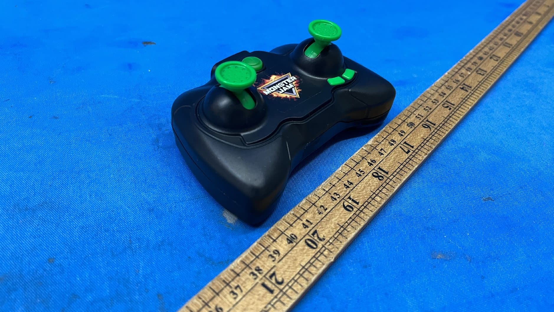
PQN66804TX2G43
Apr 03, 2024MJC Mega Grave Digger, MJC RDC Mega Grave Digger, MJC RDC Mega El Toro Loco, MNJ RDC Mega Megalodon RC, TRGT MIXED MEGA MJ HAFT PALLET, MJC COP Mega RC Asst PAL
Equipment Class
DXX - Part 15 Low Power Communication Device Transmitter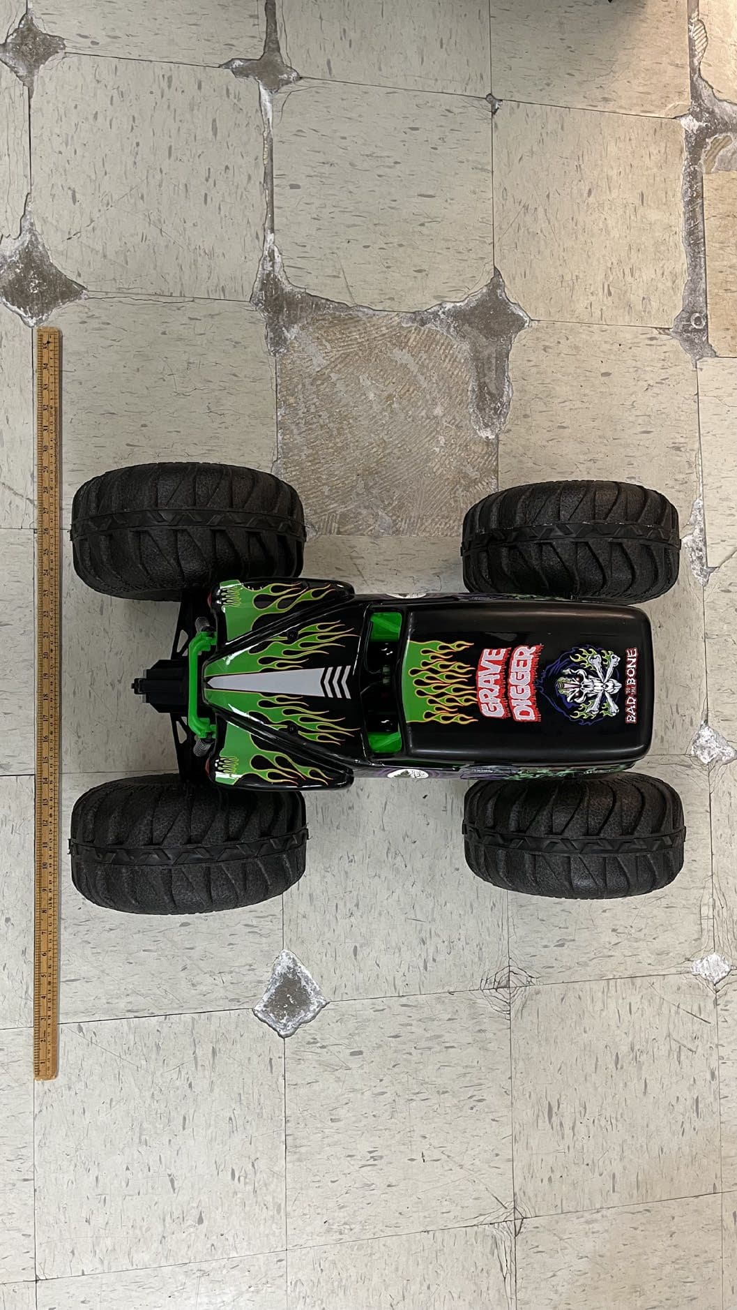
PQN66804RX2G43
Apr 03, 2024MJC Mega Grave Digger, MJC RDC Mega Grave Digger, MJC RDC Mega El Toro Loco, MNJ RDC Mega Megalodon RC, TRGT MIXED MEGA MJ HAFT PALLET, MJC COP Mega RC Asst PAL
Equipment Class
DXX - Part 15 Low Power Communication Device TransmitterPQN68126TX2G4
Aug 29, 2023HEX RDC HxmdPrSrEltStnrCrct EN GML2pkSLD
Equipment Class
DXX - Part 15 Low Power Communication Device Transmitter