PT2AG2560ADSL Wireless Router
Arescom, Inc.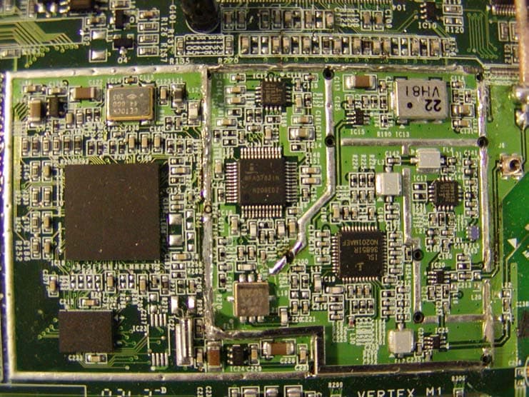
Click to zoom
Application Details
- Equipment Class
- DSS - Part 15 Spread Spectrum Transmitter
- Date of Grant
- Jun 27, 2002
- Application Purpose
- Original Equipment
- Date of Application
- Jun 27, 2002
- Equipment Note
- ADSL Wireless Router
- Frequency Range
- 2412.00000000 - 2472.00000000
- Company
- Arescom, Inc.
- Country
- United States
Documents & Files
Document Text
Text extracted from the exhibit documents filed with the FCC. Open a document above to read the original.
Users Manual
ARESCOM, INC. 3541 Gateway Blvd. Fremont, CA 94538 USA http://www.arescom.com AresGate 2560/2561 AresGate 2560/2561AresGate 2560/2561 AresGate 2560/2561 802.11b ADSL Wireless LAN Router 802.11b ADSL Wireless LAN Router802.11b ADSL Wireless LAN Router 802.11b ADSL Wireless LAN Router Software User’s Guide Software User’s GuideSoftware User’s Guide Software User’s Guide Ve r s i o n 2 . 0 June 2002 COPYRIGHT & TRADEMARKS Copyright © 2002 ARESCOM, INC. All rights reserved. ARESCOM, ARESCOM CDS are trademarks of ARESCOM, INC. Microsoft and Windows 95/98/2000/NT/Me are registered trademarks of Microsoft Corporation. Pentium is a registered trade- mark of Intel Corporation. All other trademarks and registered trademarks belong to their respective companies. ARESCOM, Inc. has the right to make revisions and to change the contents of this document without any obligation to provide prior notice of such revisions and changes. ARESCOM has the right to make improvements or changes in the product(s) and/or software(s) described in this documenta- tion. All specifications are subject to changes without notice. No part of this documentation or software may be reproduced or distributed in any form without prior written permission from ARESCOM, INC. AG2500Series Software User’s GuideJune 2002iii Table of Contents CHAPTER 1OVERVIEW 1.1Introduction .........................................................................................................................1 1.2Features ...............................................................................................................................1 1.3Package Includes .................................................................................................................1 1.4Minimum System Requirements ........................................................................................1 1.5Management Interface Options ...........................................................................................2 1.5.1HTML Interface (Web-based) ............................................................................. 2 1.5.2SNMP (Simple Network Management Protocol) ................................................ 2 1.6Network Scenario ...............................................................................................................3 CHAPTER 2HARDWARE INSTALLATION 2.1Front Panel Information ...................................................................................................... 5 2.2Back Panel Information ......................................................................................................6 2.3Location & Placement ........................................................................................................6 2.4Setup Instructions ...............................................................................................................7 CHAPTER 3BEFORE YOU START CHAPTER 4SOFTWARE CONFIGURATION 4.1Open Your Browser ..........................................................................................................11 4.2Basic - SETUP ..................................................................................................................12 4.3Basic - WIRELESS ...........................................................................................................14 4.4Basic - AUTHENTICATION ...........................................................................................16 4.5Basic - DHCP ....................................................................................................................18 4.5.1Reserved IP Table ............................................................................................. 19 4.6Basic - USER STATUS ....................................................................................................20 4.6.1Current Log-on User Status ............................................................................. 20 4.7Basic - STATUS ...............................................................................................................21 4.8Advanced - ADMINISTRATION ....................................................................................23 4.8.1Administration .................................................................................................. 23 4.9Advanced - IP ROUTING ................................................................................................25 4.9.1Current IP Routing Table ................................................................................. 25 4.9.2Add Route ......................................................................................................... 25 4.9.3Delete Route ..................................................................................................... 25 4.10Advanced - SNMP ............................................................................................................26 4.10.1Current SNMP Table ........................................................................................ 26 4.10.2Add SNMP Entry .............................................................................................. 27 4.10.3Delete SNMP Entry .......................................................................................... 27 4.11Advanced - UPGRADE ....................................................................................................28 ivAG2500Series Software User’s Guide Table of Contents CHAPTER 5TROUBLESHOOTING 5.1FAQ ..................................................................................................................................29 APPENDIX ATECHNICAL SPECIFICATIONS A.1Hardware Specifications ...................................................................................................31 A.2Software Features .............................................................................................................33 APPENDIX BSNMP SPECIFICATIONS B.1Standard Bridge MIB…
Text truncated - open the document above for the full version.
Block Diagram
AA BB CC DD EE 4 4 3 3 2 2 1 1 PCMCIAGLOBESPAN MEMORY CIRCUIT PAGE 4 DSP SDRAM BUS D). MD3: WLAN LINK/ACT(GREEN). TRANSFORMER B). CS2: LED. PAGE 81M X 8 B). MD1: ADSL LINK(GREEN). PAGE 2 C). MD2: ETHERNET LINK/ACT(GREEN). PAGE 6 A). CS0: FLASH. 2X1MX16 SNI C). CS4: SDRAM. MotorolaMPC8 50DSL CPU PAGE 7 UTOPIA BUS for WLAN PAGE 11 ARESCOM AG2560 A). MD0: DIAG (AMBER). PAGE 11 +3.3V BLOCK DIAG RAM: PCB P/N: 109000000205 Rev 1.0: INTERLEAVE AFE 1X10BT PORT E). MD4: RESERVED. LED CREATED ON Mar/20/2002 1. CHIP SELECT ASSIGMENTS: PAGE 12 EPB BUS Motorola MPC 850 CPU SINGLE BOARDAG2560 WITH GLOBESPAN 1124 PHYANNEX A PAGE 5 LED LATCH +5V GLOBESPAN PAGE 3 FLASH 10BT LAN + WLAN ( 802.11b ) MPC 850 PIN ASSIGMENTS: PAGE 9 LINE INTERFACE ESD PROTECT CIRCUIT RJ11 +12V D). UTO_CSN: ADSL PHY (INTEL MODE). PAGE 10 POWER PROTECTION 2. LED ASSIGMENTS: (ACTIVE LOW) SDRAM ETHERNET PHY PAGE 10 PAGE 11 VERSION UPDATE HISTORY : JACK- RJ45 CLOCK= 20MHz CLOCK= 4MHzSYSTEM CLOCK= 48MHz HEADER 1.0 AG2560Arescom, Inc. C 112 Monday, April 29, 2002 TitleSize Document Number Rev Date: Sheet of
External Photos
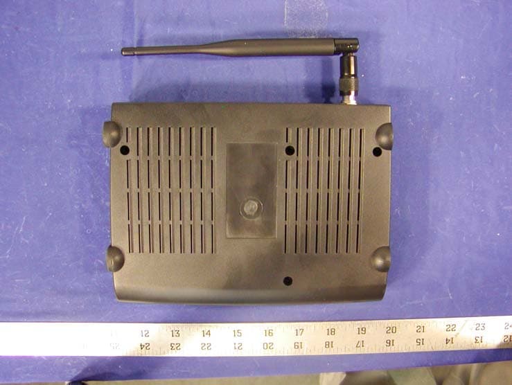
APPENDIX C - EUT EXTERNAL PHOTOGRAPHS Chassis - Front View Chassis - Rear View Chassis - Top View Chassis - Bottom View Power Adapter - Top View Main Board - Component View Main Board - Solder View RF Board - Component View
ID Label/Location Info
APPENDIX A - FCC PRODUCT LABELING AND WARNING STATEMENT FCC ID Label Proposed Label Location on EUT Bottom Side of EUT/Proposed ID Label Location FCC Warning Statement The device shall bear the following FCC statement. If the EUT is so small or for such use that it is not practicable to place the statement on it, the statement shall be placed in a prominent location in the instruction manual or pamphlet supplied to the user or, alternatively, shall be placed on the container in which the device is marketed. However, the FCC identifier or the unique identifier, as appropriate, must be displayed on the device. “This device complies with Part 15 of the FCC Rules. Operation is subject to the following two conditions: (1) this device may not cause harmful interference, and (2) this device must accept any interference received, including interference that may cause undesired operation.” This device complies with part 15 of the FCC Rules. Operation is subject to the following two conditions: (1) this device may not cause harmful interface, and (2) this device must accept any interference received, including interference that may cause undesired operations. Caution: To comply with FCC RF exposure requirements, a separation distance of at least 8 inches (20cm) must be maintained between the antenna of this and all persons. FCC ID: PT2AG12560
Internal Photos
APPENDIX C - EUT INTERNAL PHOTOGRAPHS Main Board - Component View Main Board - Solder View RF Board - Component View
Operational Description
ARESCOM NetDSL 1700 Confidential Wireless LAN ADSL Router Product Specifications V5.2 Revision 3 1 1.0 HARDWARE SPECIFICATIONS Interface WAN Interface • ADSL Interface • One ADSL port (RJ-11) • ADSL Line Code: Support ANSI T1.413 Issue 2, ITU-T G.992.1 (G.DMT), and ITU-T G.992.2 (G.Lite) • ADSL Data Rate: • ANSI T1.413: Up to 8 Mbps downstream and up to 1024 Kbps upstream operating at full rate connection • G.DMT: Up to 8 Mbps downstream and up to 1024 Kbps upstream operating at DMT full rate connection • G.Lite: Up to 1.5 Mbps downstream and up to 1024 Kbps upstream operating at G.lite connection Wired LAN Interface • One Ethernet 10BaseT (IEEE 802.3) port (RJ-45) Wireless LAN Interface • IEEE 802.11b High Rate compliant • Operating in the unlicensed 2.4GHz ISM band • Operation Frequency/Channels ( Either one below) - North America/FCC: 2.412~2.462 GHz (11 channels) - Europe/ETS: 2.412~2.472 GHz (13 channels) - Japan/TELEC: 2.412~2.472 GHz (14 channels) • Modulation Technique: Direct Sequence Spread Spectrum (CCK, DQPSK, DBPSK) • Dynamic Rate Shifting: 11, 5.5, 2 and 1Mbps • Media Access Protocol: CSMA/CA with ACK • Security Management: 40-bit, 128-bit WEP (wired equivalent privacy) Encryption • Maximum Output Power: 17dBm (50mW) Antenna Removable 3-dBi diversity high gain dipole antenna LEDs • POWER • DIAG • ADSL WAN • Ethernet • Wireless LAN Mechanical • Dimensions: 8” (w) x 5.75” (d) x 1.5” (h) ARESCOM NetDSL 1700 Confidential Wireless LAN ADSL Router Product Specifications V5.2 Revision 3 2 • Weight: 1.5 lbs. Operating Environment • Operating temperature: 0°C to 40°C (32°F to 104°F) • Operating humidity: 0% to 95% non-condensing Power External AC Power Adapter • Input: 230V 85 mA or 120V 155 mA, 47-60 Hz • Output: 13.5V AC, 1A • Power consumption: 8.5 watts nominal Compliance / Regulatory • EMI: FCC Part15 Class B & Part 15C, CE EN55022 Class B • Telecom: FCC Part 68 • WiFi Certified • Immunity: CE EN55024 • Safety: CE EN60950
Schematics
AA BB CC DD EE 4 4 3 3 2 2 1 1 PCMCIAGLOBESPAN MEMORY CIRCUIT PAGE 4 DSP SDRAM BUS D). MD3: WLAN LINK/ACT(GREEN). TRANSFORMER B). CS2: LED. PAGE 81M X 8 B). MD1: ADSL LINK(GREEN). PAGE 2 C). MD2:ETHERNET LINK/ACT(GREEN). PAGE 6 A). CS0: FLASH. 2X1MX16 SNI C). CS4: SDRAM. MotorolaMPC8 50DSL CPU PAGE 7 UTOPIA BUS for WLAN PAGE 11 ARESCOM AG2560 A). MD0: DIAG (AMBER). PAGE 11 +3.3V BLOCK DIAG RAM: PCB P/N: 109000000205 Rev 1.0: INTERLEAVE AFE 1X10BT PORT E). MD4: RESERVED. LED CREATED ON Mar/20/2002 1. CHIP SELECT ASSIGMENTS: PAGE 12 EPB BUS Motorola MPC 850 CPU SINGLE BOARDAG2560 WITH GLOBESPAN 1124 PHYANNEX A PAGE 5 LED LATCH +5V GLOBESPAN PAGE 3 FLASH 10BT LAN + WLAN ( 802.11b ) MPC 850 PIN ASSIGMENTS: PAGE 9 LINE INTERFACE ESD PROTECT CIRCUIT RJ11 +12V D). UTO_CSN: ADSL PHY (INTEL MODE). PAGE 10 POWER PROTECTION 2. LED ASSIGMENTS: (ACTIVE LOW) SDRAM ETHERNET PHY PAGE 10 PAGE 11 VERSION UPDATE HISTORY : JACK- RJ45 CLOCK= 20MHz CLOCK= 4MHzSYSTEM CLOCK= 48MHz HEADER 1.0 AG2560Arescom, Inc. C 112 Monday, April 29, 2002 TitleSize Document Number Rev Date: Sheet of AA BB CC DD EE 4 4 3 3 2 2 1 1 MODE 0 1. VALUES OF R12, R13, R4, R7 AND C9 DEPEND ON THE LINEDRIVER, U1. THIS SCHEMATIC SHOWEN THE VALUES WHHILEU1=EL1509C. SEE NOTE 4 2. USE 100MIL SPACING FOR DIFFERENTIAL TEST POINT PAIRS. SEE NOTE 4 SEE N OTE 1 SHEET NOTES: DMT Annex A U505 MODE SWITCH: SEE NOTE 2 0 BYPASS SEE NOTE 4 SEE NOTE 1 APPLICATION 1 For Annex A/B:DNP U3 AND R19=R30=0R.For Annex C:INSTALL U3 ANDR19=R30=OPEN. PHY_LINE_INTERFACE 1.0 AG2560Arescom, Inc. C 212 Monday, April 29, 2002 TitleSize Document Number Rev Date: Sheet of OUTA INA+INB- INB+INA- VS/2 VS/2 OUTB RCVFP 3RCVFN 3DMT_MODE_0 5 TXFLN 3 TXFLP 3 ATTEN 5 SIG2 6SIG1 6 A A A +12VA +12VA A +5VA A A A +12VA A +12VA A A A A A +12VA A +5VA A +12VA A A +12VA A A A +12VA +12VA A A R28422 L4DNE R25422 C18 560PF C1 10UF R45 10K L8 680UH R18 487 R3 10 L2 680UH C3 560PF R8 10 C14 DNE R33 499 TP8 R35 845 R20 499 R13 2K C130.1uF U3 OPEN/MAX4525CUB 29 1387 456 10 COMACOMB NOANCANOBNCB INH GND ADD V+ C35 DNE TP7 R34 845 TP11 C38 1200PF R31 499 R3249.9,1% C23 1200PF GFP4 0R\S8 R1 5.11K TP9 R21 845 R94.99K C31 FOOTPRINT/OPEN C362DNE C111500PF C324700PF TP10 R46 DNE C16 1UF GFP70R\S8 C271500PF R23 10 C100.1uF TP1 C450.1uF R24 499 L7 680UH TP2 C5 1UF R4 0R R7 619 C9DNE TP4 R29 10 C360.1uF R17 DNE C208200PF R39 0R\S8 TP6 D2 B E C C7 0.12UF R27.5KR264.99K GFP4X OPEN C210.1uF R274.99K R16100\S8 GFP80R\S8 D1 B E C C346A1 FOOTPRINT/OPEN GFP5 0R\1206 R6 4.99K +- U4B 56 7 84 TP3 C306800PF + - AB + - V+V- U1 EL1509C 2356 17 84 C430.1uF C19 FOOTPRINT/OPEN C34 0.1uF C29 FOOTPRINT/OPEN C44 DNE C20.1uF L6 680UH C370.1uF C26 3300PF GFP2 348 GFP1812/0603 R12 2K TP5 C41 3300PF L5DNE GFP1 348 GFP1812/0603 + - U2AEL2270C 32 1 84 U5 MAX4541CSA 1 26 573 84 NO1 COM1COM2 NO2IN1IN2 V+ GND GFP30.01UF R117.5K C170.1uF C22 DNE R54.75K C122700PF +- U2BEL2270C 56 7 84 R42 0R L1 10UH R44 DNE C330.018UF GFP7X OPEN R19 0R R41 0R\S8 C42 DNE R104.75K R374.99K L9DNE C40 1800PF R22 845 GFP8X OPEN C150.1uF R36 4.99K R38 422 C345A1 FOOTPRINT/OPEN C39 1800PF C28 0.1uF R14 5.11K Q1 DNE R30 0R R40 422 C4 0.1uF GFP6 0R\1206 + - U4A EL2227C 32 1 84 C80.033UF C24 1800PF GFP6X OPEN L3 680UH C25 1800PF R43 0R\S8 GFP5X OPEN R15100\S8 . ... T1 C1601 1 10 4 7 2 9 5 6 AA BB CC DD EE 4 4 3 3 2 2 1 1 50 8 34 PIN # AFE 41 70 1. PLACE R49 AS CLOSE TO U6 AS POSSIBLE. PIN # AFE 3. INDUCTOR L10 AND ASSOCIATED CAPACITOR SHOW ONE METHOD TO DERIVE +5VA FROM +5VD. PIN # 29 78 SHEET NOTES: AFE SEE NOTE 3 18 AFE 49 SEE NOTE 1 19 9 PHY_AFE 1.0 AG2560Arescom, Inc. 312 Monday, April 29, 2002 TitleSize Document Number Rev Date: Sheet of PDO6PDI7PDO0PDO3PDI6PDO2PDO8PDO5 PDI[0..11] PDI2PDI9PDO10PDO4PDI5PDI10PDI0 PDO[0..11] PDI4PDO9PDO7PDI1PDI3PDI8PDI11PDO11PDO1 PDI[0:11] 5 RCVFP 2RCVFN 2 A2DCKA 5 D2ACKA 5 CSCKA 5 PDO[0..11] 5 CSDOA 5 TXFLN 2TXFLP 2 A D +5VD +5VA +3.3VD A +5VD D A +5VA +5VD +5VA +3.3VD D D A C500.1uF C510.1uF C48 0.1uF R4725.5K U6 686766656463626160595857568371 282238373132121110 879091939596979899 456 4243151620 77 40 79 85 55 69 14 17 30 33 39 47 9 18 19 29 34 41 49 21 78 50 70 8 TXD11TXD10TXD9TXD8TXD7TXD6TXD5TXD4TXD3TXD2TXD1TXD0TXCLKRCVCLKCSCLK PGAIP PGAIN RCFLP RCFLN RCFLOP RCFLON VCM VREFPQ VREFNQ RCVD11RCVD10RCVD9RCVD8RCVD7RCVD6RCVD5RCVD4RCVD3RCVD2RCVD1RCVD0 DACOUTP DACOUTN ADP ADN AAFLN CSD VB1 GNDD GNDD GNDD GND3V GNDA GNDA GNDA GNDA GNDA GNDA VDDA VDDA VDDA VDDA VDDA VDDA VDDA AAFLP VDDD VDDD VDD3V VDDD TP16 C570.1uF . C550.1uF TP18 C580.1uF C590.1uF C49 0.1uF TP19 R49 0R\S8 C600.1uF C610.1uF TP17 C620.1uF C46 0.1uF C630.1uF C640.1uF C650.1uF C660.1uF TP14 L103.3UH C47 0.1uF TP15 C670.1uF C540.1uF C530.1uF C56 4.7UF C52 0.1uF R4825.5K AA BB CC DD EE 4 4 3 3 2 2 1 1 RSAD6 RSA13RSAD3 FROM PIN 47 (INTB) OF DSP INTERLEAVING MEMORY PIN/F UNCTION ASSIGNMENTS: RSWRN TA[16] = ALE RSAD1 RSA12RSA8RSAD4RSAD5RSAD1RSAD7CEN INTERLEAVING MEMORY RSAD0 TA[8..15], RSA16 = ADDRESS[8..16] RSAD7 RSA10 FROM PIN 56 (DCO) OF DSP TA2, TA[5..7], RSAD4, TA[17..19] = ADDRESS[0..7] RSRDN RSAD2 RSAD2 TA[3] = CEN FROM TA BUS OF DSP RSA9 INTB = RSRDNDCO = RSWRN RSAD0RSA14RSA11 RSAD3 FROM PIN 61 (A4) OF DSP RSAD5 RSAD4 RSAD6 PHY_INTLVMEM 1.0 AG2560Arescom, Inc. 412 Monday, April 29, 2002 TitleSize Document Number Rev Date: Sheet of TA18 TA18 TA3 TA17 TA2 TA19 TA8TA9TA13 RSA0RSA2 TA6 RSA3 TA14 TA19TA17TA6 TA10TA12 RSA7RSA6 TA16 TA[2..19] TA5 RSA4 TA7 A4 RSA5 TA7 TA2 TA11 RSA1 TA5 RSAD4 5 TA[2:19] 5 INTB 5 DCO 5 D D +3.3VD +3.3VD +3.3VD D C690.1uF R50 100\S8 R51 4.99K C680.1uF U8 IS61LV256 10 9876543 25242123 2 26 1 202227 11121315161718192814 A0A1A2A3A4A5A6A7A8A9A10A11A12A13A14CE OEWE I/O0I/O1I/O2I/O3I/O4I/O5I/O6I/O7 VCC GND U774LVC573 23456789 11 1 1918171615141312 D0D1D2D3D4D5D6D7LEOE Q0Q1Q2Q3Q4Q5Q6Q7 AA BB CC DD EE 4 4 3 3 2 2 1 1 53 LAYOUT NOTES: 20 88 SHEET NOTES: 109 20 102 DSP LABEL TP35 AS 'DGASP' SEE NOTE 1 37 PLACE CLOSE TO U9. STROBE RESISTORSSHOULD BE PLACED CLOSE TO U9. DCOROUTE SHOULD BE KEPT AS SHORT ASPOSSIBLE TO NOT INTERFERE WITHINTERLEAVING …
Text truncated - open the document above for the full version.
Test Report
Note: This test report is specially limited to the above client company and product model only. It may not be duplicated without prior written consent of Bay Area Compliance Laboratory Corporation. This report must not be used by the client to claim product endorsement by NVLAP or any agency of the U.S. Government. FCC PART 15 SUBPART C EMI MEASUREMENT AND TEST REPORT For Arescom, Inc. 3541 Gateway Blvd. Fremont, CA 94538 FCC ID: PT2AG2560 June 21, 2002 This Report Concerns: Original Report Equipment Type: ADSL Wireless Router Test Engineer: Benjamin Jing Report No.: R0205068 Test Date: May 6, 2002 Reviewed By: Jeff Lee Prepared By: Bay Area Compliance Laboratory Corporation 230 Commercial Street Sunnyvale, CA 94085 Tel: (408) 732-9162 Fax: (408) 732 9164 Arescom, Inc. FCC ID: PT2AG2560 Report # R0205068Rpt Page 2 of 26 FCC Part 15.247 Test Report TABLE OF CONTENTS 1 - GENERAL INFORMATION..................................................................................................................................4 1.1 PRODUCT DESCRIPTION FOR EQUIPMENT UNDER TEST (EUT) ..............................................................................4 1.2 OBJECTIVE.............................................................................................................................................................4 1.3 TEST METHODOLOGY............................................................................................................................................4 1.4 TEST FACILITY.......................................................................................................................................................4 1.5 TEST EQUIPMENT LIST...........................................................................................................................................5 1.6 LOCAL SUPPORT EQUIPMENT LIST AND DETAILS...................................................................................................5 1.7 EXTERNAL I/O CABLING LIST AND DETAILS.........................................................................................................5 2 - SYSTEM TEST CONFIGURATION AND REQUIREMENT............................................................................6 2.1 DESCRIPTION OF TEST CONFIGURATION................................................................................................................6 2.2 EQUIPMENT MODIFICATION...................................................................................................................................6 2.3 CONFIGURATION OF TEST SYSTEM.........................................................................................................................6 2.4 TEST SETUP BLOCK DIAGRAM...............................................................................................................................6 3 - SUMMARY OF TEST RESULTS..........................................................................................................................7 4 - CONDUCTED OUTPUT POWER.........................................................................................................................8 4.1 STANDARD APPLICABLE........................................................................................................................................8 4.2 MEASUREMENT PROCEDURE..................................................................................................................................8 4.3 MEASUREMENT RESULT........................................................................................................................................8 4.4 TEST EQUIPMENT...................................................................................................................................................8 5 - SPURIOUS EMISSION.........................................................................................................................................10 5.1 STANDARD APPLICABLE......................................................................................................................................10 5.2 MEASUREMENT PROCEDURE................................................................................................................................10 5.3 MEASUREMENT DATA..........................................................................................................................................10 6 - 6 DB BANDWIDTH OF EMISSIONS .................................................................................................................14 6.1 STANDARD APPLICABLE......................................................................................................................................14 6.2 MEASUREMENT PROCEDURE................................................................................................................................14 6.3 MEASUREMENT DATA..........................................................................................................................................14 7 - 100 KHZ BANDWIDTH OF BAND EDGES ......................................................................................................16 7.1 STANDARD APPLICABLE......................................................................................................................................16 7.2 MEASUREMENT PROCEDURE................................................................................................................................16 7.3 TEST RESULTS.....................................................................................................................................................16 8 - POWER DENSITY ................................................................................................................................................18 8.1 STANDARD APPLICABLE.........................................................................................................…
Text truncated - open the document above for the full version.
Test Setup Photos
APPENDIX B - TEST SETUP PHOTOGRAPHS Conducted Emission - Front View Conducted Emission - Rear View Radiated Emission - Front View Radiated Emission - Rear View
Contact Information
Applicant
James Lu(Senior Hardware Manager)
Test Firm
Bay Area Compliance LaboratoryJohn Chan
Technical Specifications
| # | Rule Parts | Frequency Range | Power Output |
|---|---|---|---|
| 1 | 15C | 2.41 GHz - 2.47 GHz | 43.00 mW |
Other Applications from Arescom, Inc.
PT2AG2000S
Jun 25, 2002802.11b Wireless LAN Router
Equipment Class
DSS - Part 15 Spread Spectrum Transmitter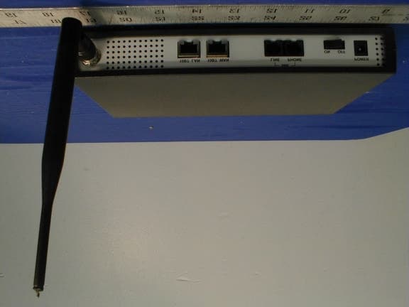
PT2AG1000PRO
Oct 22, 2001AresGate 1000 Wireless Router
Equipment Class
DSS - Part 15 Spread Spectrum Transmitter