PY3WGR615VV2Wireless VoIP Router
Netgear Incorporated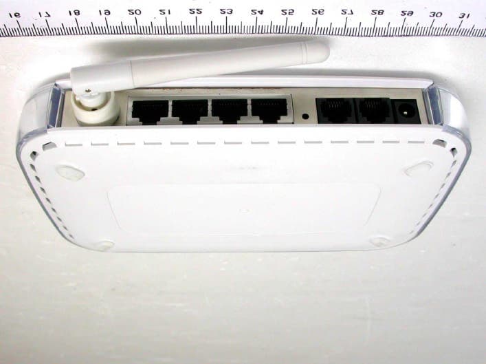
Click to zoom
Application Details
- Equipment Class
- DTS - Digital Transmission System
- Date of Grant
- Apr 27, 2005
- Application Purpose
- Original Equipment
- Date of Application
- Apr 27, 2005
- Equipment Note
- Wireless VoIP Router
- Frequency Range
- 2412.00000000 - 2462.00000000
- Company
- Netgear Incorporated
- Country
- United States
Documents & Files
Document Text
Text extracted from the exhibit documents filed with the FCC. Open a document above to read the original.
Users Manual
September 2004 1.0 Version 1.0 September 2004 NETGEAR, Inc. 4500 Great America Parkway Santa Clara, CA 95054 USA Wireless VoIP WGR615VV2 Manual ii September 2004 © 2004 by NETGEAR, Inc. All rights reserved. September 2004. Trademarks NETGEAR is a trademark of Netgear, Inc. Microsoft, Windows, and Windows NT are registered trademarks of Microsoft Corporation. Other brand and product names are registered trademarks or trademarks of their respective holders. Statement of Conditions In the interest of improving internal design, operational function, and/or reliability, NETGEAR reserves the right to make changes to the products described in this document without notice. NETGEAR does not assume any liability that may occur due to the use or application of the product(s) or circuit layout(s) described herein. Federal Communications Commission (FCC) Compliance Notice: Radio Frequency Notice This equipment has been tested and found to comply with the limits for a Class B digital device, pursuant to part 15 of the FCC Rules. These limits are designed to provide reasonable protection against harmful interference in a residential installation. This equipment generates, uses, and can radiate radio frequency energy and, if not installed and used in accordance with the instructions, may cause harmful interference to radio communications. However, there is no guarantee that interference will not occur in a particular installation. If this equipment does cause harmful interference to radio or television reception, which can be determined by turning the equipment off and on, the user is encouraged to try to correct the interference by one or more of the following measures: •Reorient or relocate the receiving antenna. •Increase the separation between the equipment and receiver. •Connect the equipment into an outlet on a circuit different from that to which the receiver is connected. •Consult the dealer or an experienced radio/TV technician for help. Customer Support Refer to the Support Information Card that shipped with your Wireless Router. CAUTION: 1) To comply with FCC RF exposure compliance requirements, a separation distance of at least 20 cm must be maintained between the antenna of this device and all persons. 2) This transmitter must not be co-located or operating in conjunction with any other antenna or transmitter. Changes or modifications not expressly approved by the party responsible for compliance could void the user's authority to operate the equipment. Users Information September 2004 iii September 2004 iv Contentsv September 2004 Contents Chapter 1 About This Guide Audience, Conventions, and Formats ............................................................................1-1 Tips for Printing This Manual ..........................................................................................1-2 Chapter 2 Getting to Know Your NETGEAR Wireless Router Package Contents ..........................................................................................................2-1 The Front Panel .......................................................................................................2-2 The Rear Panel ........................................................................................................2-3 Chapter 3 Connecting the Router to the Internet Prepare to Install Your Wireless Router ..........................................................................3-1 First, Connect the Wireless Router to the Internet .........................................................3-1 Now, Set Up a Computer for Wireless Connectivity .......................................................3-6 Troubleshooting Tips ......................................................................................................3-7 Overview of How to Access the Wireless Router ...........................................................3-8 How to Log On to the Wireless Router After Configuration Settings Have Been Applied ..............................................................3-9 How to Bypass the Configuration Assistant ...........................................................3-10 How to Manually Configure Your Internet Connection ..................................................3-10 Using the Smart Setup Wizard .....................................................................................3-12 NETGEAR Product Registration, Support, and Documentation ...................................3-13 Chapter 4 Optimizing Wireless Connectivity and Security Observe Performance, Placement, and Range Guidelines ............................................4-1 Implement Appropriate Wireless Security ......................................................................4-2 Understanding Wireless Settings ...................................................................................4-3 Information to Gather Before Changing Basic Wireless Settings .............................4-6 Default Factory Settings ...........................................................................................4-7 September 2004 viContents How to Set Up and Test Basic Wireless Connectivity ..............................................4-7 How to Configure WEP ............................................................................................4-9 How to Configure WPA-PSK Wireless Security ............................................................ 4-11 How to Restrict Wireless Access by MAC Address ...................................................... 4-11 Chapter 5 Doing Basic Router Housekeeping Changing the Administrator Password ...........................................................................5-1 Configuration File Management .....................................................................................5-2 Restoring and Backing Up the Configuration ...........................................................5-2 Erasing the Configuration .................................................…
Text truncated - open the document above for the full version.
Cover Letter(s)
April 6, 2005 Federal Communications Commission Authorization and Evaluation Division FCC ID : PY3WGR615VV2 Confidentiality Request Pursuant to Sections 0.457 and 0.459 of the Commission’s Rules, the Applicant Hereby requests confidential treatment of information accompaniment this Application As outlined below: 1. Block Diagram, 2. Schematic Diagram, The above materials contain trade secrets and proprietary information not customarily released to the public. The public disclosure of these matters might be harmful to the Applicant and provide unjustified benefits to its competitors. The Applicant understands that pursuant to Rule 0.457, disclosure of this Application and all accompanying documentation will not be made before the date of the Grant for this application Sincerely, Larry Kerila / Product Design Manager Applicant: Netgear, Inc. Address: 4500 Great America Parkway, Santa Clara, California 95054 USA TEL: +1-408-907-8000 FAX: +1-408-907-8097
Cover Letter(s)
Federal Communications Commission Dear Sir, We, the undersigned, hereby authorize Exclusive Certification Corp. to act on our behalf in all matters relating to application for Wireless VoIP (Model: WGR615VV2, FCC ID No.: PY3WGR615VV2)” authorization, including the signing of all documents relating to these matters. Any and all carried out by Exclusive Certification Corp. on our behalf shall have the same effect as acts of our own. The applicant certifies that in the case of an individual applicant (e.g., corporation), no party to the applicant is subject to a denial of federal benefits, that includes FCC benefits, pursuant to section 5301 of the Anti-drug abuse Act of 1988.21 U.S.A. 862. For a definition of a “party” for these purposes See 47 C.F.R. 1.2002(b). By: By: Larry Kerila (Signature) (Printed) Title: Product Design Manager Applicant: Netgear Inc. Address: 4500 Great America Parkway, Santa Clara, California 95054 USA Tel: +1-408-907-8000 Fax: +1-408-907-8097 E-mail: [email protected] Date: April 6, 2005
Cover Letter(s)
Statement Federal Communications Commission To whom it may concern, We, NetGear Inc., have done some modifications during testing the product of FCC ID: PY3WGR615VV2, and we hereby declare that this modification will be implemented in the final product. By: Larry Kerila Title: Product Design Manager Applicant: Netgear, Inc. Address: 4500 Great America Parkway, Santa Clara, California 95054 USA Tel: +1-408-907-8000 Fax: +1-408-907-8097 E-mail: [email protected] Date: Jan. 07, 2004
Cover Letter(s)
Exclusive Certification Corp. 4F-2, No. 28, Lane 78, Xing-Ai Rd. Nei-hu, Taipei City 114 Taiwan R.O.C 11478284-2F Tel: 886-2-2792-3366 Fax: 886-2-2792-1100 To whom it may concern The enclosed documents constitute a formal submittal and application for a Grant of Equipment Authorization pursuant to Subpart C of Part 15 of FCC rules (CFR47) regarding Wireless VoIP for the Netgear model WGR615VV2. Data within this report demonstrates that the equipment tested complied with the FCC limits for intentional radiators. Exclusive Certificate Corp. (ECC), as duly authorized agent prepared this submittal. A copy of the letter of our appointment as agent is enclosed. If there are any questions or if further information is needed, please contact ECC for assistance. Ivy Chen TEL: +886-2-2792-3366 # 204 FAX: +886-2-2792-1100 E-mail: [email protected]
Cover Letter(s)
American Telecommunications Certification Body Inc. 6731 Whittier Ave, McLean, VA 22101 April 25, 2005 RE: Netgear Inc. FCC ID: PY3WGR615VV2 I have a few comments on this Application. Depending on your responses, kindly understand there may be additional comments. 1.) The required information to the user information of 15.21 appears to be missing. Kindly review the Manual 2.) Please confirm if the copper tape and ferrites seen in the Internal Photographs will be used on all production products. Kindly supply photographs of the final electrical and mechanical fixes used on all production units. William H. Graff President and Director of Engineering mailto: [email protected] The items indicated above must be submitted before processing can continue on the above referenced application. Failure to provide the requested information may result in application termination. Correspondence should be considered part of the permanent submission and may be viewed from the Internet after a Grant of Equipment Authorization is issued. Please do not respond to this correspondence using the email reply button. In order for your response to be processed expeditiously, you must submit your documents through the AmericanTCB.com website. Also, please note that partial responses increase processing time and should not be submitted. Any questions about the content of this correspondence should be directed to the sender.
External Photos
External Photos
Internal Photos
Internal Photos
Operational Description
WGR615VV2 Operation Principle 1. CPU, U15, TNETV1060 have a 32-bit RISC processor integrated, operation frequency is 125MHz. It needs an external 25MHz crystal for system reference frequency, and an 8.192MHz crystal for telephony interface reference frequency. This chip is responsible to control Flash/SDRAM IC, CODEC IC and LED. This chip also has two integrated 10/100 Ethernet MAC/PHY. 2. FLASH: U4, MX29LV320ABTC, 4Mbytes Flash, and 90ns. It is used to store the normal and test firmware. 3. Wireless q RC2326(U2): IEEE 802.11 b/g RFFE ISM Band, highly integrated 802.11 b/g radio Radio, fully integrated up/down converters, LNA, PA, TX detector and T/R switches q RC2422(U8): IEEE 802.11 b/g IQ/IF Transceiver With Dual VCO Synthesizers, Highly integrated 802.11 b/g radio IQ/IF Transceiver PLL ASIC, Fully integrated IF and RF VCOs and synthesizer q (U1)TNETW1130GVF Wireless MAC and Baseband processor 4. Switching Controller: U6, MARVELL88E6060. It is used to provide 4 ports of ethernet interface. 5. CODEC, U9/U10, Si3210-KT, Programmable CMOS SLIC/CODEC. They provide 2 channel VOIP function. 6. Power part: several regulators are used on the board. U12, FP5452 is used to generate 3.3V and 2.5V DC voltage from 12V DC power input. Q9/Q16/Q17 is used to generate 1.6V DC voltage from 3.3V DC power, and 1.6V is CPU core voltage. U1 is used to generate 1.5V DC voltage from 3.3V DC power, and 1.5V is Switch core voltage. 7. Switch button, S1, it is used to factory restore or system reboot.
RF Exposure Info
1.1. Test Result of RF Exposure Evaluation . Product: Wireless VoIP . Test Item: RF Exposure Evaluation Data . Test site: OATSI-SD . Test Mode: Normal Operation 1.1.1. Antenna Gain The maximum Gain is 2.0 dBi. 1.1.2. EUT Operation condition Software provided by client enabled the EUT to transmit and receive data at lowest, middle and highest channel individually. 1.1.3. Output Power into Antenna & RF Exposure Evaluation Distance Modulation Standard: IEEE 802.11b Test Date: February 25, 2005 Temperature: 23 Humidity: 59 Channel Channel Frequency (MHz) Output Power to Antenna (dBm) Power Density (S) (mW/cm 2 ) 01 2412 14.89 0.0100 06 2437 14.77 0.0100 11 2462 14.89 0.0100 Modulation Standard: IEEE 802.11g Test Date: February 20, 2005 Temperature: 23 Humidity: 59 Channel Channel Frequency (MHz) Output Power to Antenna (dBm) Power Density (S) (mW/cm 2 ) 01 2412 14.73 0.0100 06 2437 14.82 0.0100 11 2462 14.81 0.0100 The MPE is calculated as 0.0100 mW / cm 2 < limit 1 mW / cm 2 . So, RF exposure limit warning or SAR test are not required.
Schematics
11 22 33 44 55 66 77 88 A A B B C C D D VERSION DESCRIPTION CHANGE HISTORY WGR615V V2 DATE 0.1 03/06/2004 DRAFT PCB Number CONFIDENTIALPRELIMINARY BOARD ID:0520384900R800 0.1 CHANGE HISTORY C 113 , 22, 2005 SERCOMM CORP. WGR615VV2 4900R800 TitleSize Document Number Rev Date: Sheet of 55 44 33 22 11 D D C C B B A A CONFIDENTIAL 3.3V 2A LOW ESR 12V 1.2A RESET CIRCUIT 2.5V 2A SWITCH CORE SUPPLY Place it near to Switch 0.1 Main Power C 213 , 22, 2005 SERCOMM CORP. WGR615VV2 4900R800 TitleSize Document Number Rev Date: Sheet of FB1_V OUT2_V 1N2P_V DTC1_V PWR1 OUT1_V IN1N_V 12V DTC2_V F1P2 1N2N_V REF_V FB2_V IN1P_V PWR2 CHK1in OPAout CHK2in PWR3 CHK1inCHK2in CHK1outCHK2outCHK1out /RESET_IN CHK2out OPAin PWR3 OPAin OPAout REF2.5V 20MIL_1V5 VDDVDD VDDT VCC VDD_AIC VDDT VDD_PHY VDDT 3.3V INPOWER VDD_PCI 12V 2.5V VDD VCC 12V 3V3_S VDD VDD VDD_SLIC VDD 2V5VDD INPOWER 3V3_S 1V5 R9210K + C23410uF/10V/NC C1051000pF/NC D5 SK34/NC 12 C971uF C1660.1uF J3 POWERJACK2.0 123 C1570.1uF C1581000pF R21933K C2051000pF L1 BEAD4S/NC 2 3 1 4 C113 0.1uF C223 0.1uF/NC + C54 10uF/10V C2180.1uF R221 10K C2301uF R8750-1% FB370-805 1 2 C235330pF R22610K L3 33uH C780.1uF R16533K + C151 10uF/10V/NC R227 220K C1160.1uF FB2 0-805 1 2 FB330-805 1 2 R21833K R24710K FB1FBEAD/NC + C20 470uF/10V U1AP1117-ADJ 3 2 1 4 IN OUT GND TAB D6SCD34 C80.1uF Q19LM431/SOT 31 2 FB60-805 R1674.7K C186 0.1uF/NC Q18EM6353-2.9 1 2 3 GND RES 3.3V R20520K + C41 0.22uF C187 0.1uF C38 330pF C1471000pF C37 0.22uF FB380-805 1 2 FB4FBEAD/NC C1680.1uF/NC U2 9435M 123 4 8765 R16410K C421uF D3 SCD34 C1390.1uF C1520.1uF/NC C2100.1uF C470.1uF C2310.1uF U129435M 1 2 3 4 8 7 6 5 C1151000pF + C3 10uF/10V C621000pF + C13810uF/10V/NC R251 0 FB350-805 1 2 R938.2K-1% FB50-805 C2360.1uF/NC R2460 + C213 10uF/10V R22933K C1190.1uF/NC L8 33uH + C40 470uF/10V C2321000pF + C23310uF/10V/NC R9150-1% R22833K + C132 10uF/10V/NC + C181 10uF/10V R16610K FB220-805 1 2 FB300-805 1 2 FB210-805 1 2 R2060 R217 220K R8310K C2020.1uF + C15510uF/10V C222 0.1uF U16 FP5452 12345678 910131115141216 CTRT1IN+1IN-1FB1DTC1OUTGND VCC 2OUT 2IN- 2DTC SCP 2IN+ 2FB REF FB340-805 1 2 U3 9435M 123 4 8765 C1790.1uF + C108 10uF/10V L2 BEAD4P/NC 2 4 1 3 + C21470uF/25V R22012K D4 SK34/NC 12 R2524.7K R253 100K F1RLD30P135U -+ U7ALM358 32 1 84 FB30-805 1 2 C20.1uFR916.8K-1% C1060.1uF/NC C2190.1uF/NC C159330pF C1140.01uF U179435M 1 2 3 4 8 7 6 5 SW_RST 6 /RESET_IN 6 55 44 33 22 11 D D C C B B A A PRELIMINARYCONFIDENTIAL RX2R128 0 OHM RX4 4.7K OHM RX1 0 OHMNC RX5 0 OHMNC 0 OHM 28F320C3TA100 NC AMD29LV640DB90 4.7K OHM 0 OHM R46U6 NC RX3 0 OHMNC NC U6.37 U6.13 U24.9 U24.37 U24.43 U24.15 U6.37 U24.9 4900R800 0.1 FLASH C 313 , 22, 2005 SERCOMM CORP. WGR615V V2 TitleSize Document Number Rev Date: Sheet of D8 A15A22A12 D13 A4 D10D2D6D7 A21A14A8A9A17A13A11 D0D1D15D14 A5 D12D4 A10A20A3A19 D3D5 A18 D9 A16A2 D11 A0A6A7A1A23 D1 A3 D0D5 A18A6A17A1 D9D10 A13A11A5A20A0 D[31..0] D7D11 A10A23 D6 A7A2 D4 A14A4 D12 A12 D14D15D8D13 A19 A[23..0] A16 D2 /FLASH_WP A15A8A9 D3 VDD VDD VDD VDD VDD VDD VDD VDD C1670.1uF/NC RX1 0/NC C1560.1uF C1340.1uF C22610uF/10V/NC R4710K/NC C1350.1uF/NC RX2 0/NC U5 E28F128J3A/NC 5678 1011121317181920222324252627283216 52504745413936345149464440383533 42 48 431 3056 142295455533115 9 43 37 21 A19A18A17A16A15A14A13A12A11A10A9A8A7A6A5A4A3A2A1A0RESET D15D14D13D12D11D10 D9D8D7D6D5D4D3D2D1D0 GND GND A20A21A22A23A24 CE0 CE1CE2 OE WE STATUS BYTE VPEN VCC VCCQ VCC GND R129 4.7K U4 AMD29LV320DB 3729313335384042443032343639414345 2628114712 274615 10132524232221201918 87654321 481716 9 14 VCC D0D1D2D3D4D5D6D7D8D9 D10D11D12D13D14 D15/A-1 CE OEWEBYTERESET VSSVSS RY/BY A20A21A0A1A2A3A4A5A6A7A8A9A10A11A12A13A14A15A16A17A18A19 WP/NC R128 4.7K R404.7K/NC R46 4.7K C1910.1uF/NC RX3 0 RX4 0/NC RX5 0 R57 4.7K/NC C16210uF/10V/NC C1690.1uF/NC A[23:0] 5 D[31:0] 4,5 /SYS_RESET 6,9 FLASH_/CS0 5/WE 5 /OE 5 FLASH_/CS0 5 /WE 5 /OE 5 /SYS_RESET 6,9 D[31:0] 4,5 A[23:0] 5 55 44 33 22 11 D D C C B B A A PRELIMINARYCONFIDENTIAL U4.1 U4.9 U4.49 U5.1 U5.27 U4.9 U5.9 U5.75 U5.81 U5.3 U5.1 U5.49 U5.35 U5.55 U5.43 4900R800 0.1 SDRAM C 413 , 22, 2005 SERCOMM CORP. WGR615V V2 TitleSize Document Number Rev Date: Sheet of SDRAM_/CS1DQM0SDRAM_CLK/WE DQM2 SDRAM_CKE DQM3 /CASDQM1 /RAS/WEDQM0/CAS /RAS DQM1SDRAM_/CS1 /CAS/WESDRAM_CLKDQM3SDRAM_/CS1DQM2/RAS SDRAM_CLK SDRAM_CKE D[31..0] D11 A9 D31 A8 D4 A22 A12 D29 DQM1 A11 D11 A4 D30 D3 D27 /RAS A9A4 D17 D8 A3 A23 D14 D23 A7 D2 D24D8D15 D13 A8 A7 A6 SDRAM_CLK D6D30D29 A7 A[23..0] D24 A9A6 D7 A11 D19 D10 A1 SDRAM_CKE A10 D23 D[31..0] A2A1 D17 D10D13D4 A22 A[23..0] D16 A5 A8 A12 D6 DQM3DQM0 A3 D1D0 A5 D31 SDRAM_/CS1 D20 A11 A22 D9 D3 A1 D21D18 A10 D15D5 SDRAM_CKE /WEDQM2 A3 A6 D19 A23 D22 A0 D18D28 A10 /CAS D26 A0 D25 A0A5 D26 D12 A2 D12 A2 D2D16 A4 D7 D20 D5D14D27 A23 D22D25D21 D1D0 D9D28 SDRAM_CLK 5 VDD VDD VDD VDD VDD VDD VDD C1920.1uF C140.1uF/NC C600.1uF/NC C18910uF/10V C1700.1uF C13710uF/10V/NC C1360.1uF/NC C2250.1uF/NC C1940.1uF/NC 4MX32-TSOP86/NCU14 2526276061626364656624236867201918712817 245781011137476777980828385 1 3 9 35 41 29 44 6 12 32 38 72 43 15 31333436373940424547485051535456 221659 58 86 46 52 78 84 49 55 75 81 21 A0A1A2A3A4A5A6A7A8A9A10/APBS1CLKCKECS RASCASDQM1DQM2WE DQ0DQ1DQ2DQ3DQ4DQ5DQ6DQ7DQ8DQ9 DQ10DQ11DQ12DQ13DQ14DQ15 VCC VCCQ VCCQ VCCQ VCCQ VCC VSS VSSQ VSSQ VSSQ VSSQ VSS VCC VCC DQ16DQ17DQ18DQ19DQ20DQ21DQ22DQ23DQ24DQ25DQ26DQ27DQ28DQ29DQ30DQ31 BS0DQM0DQM3 VSS VSS VSSQ VSSQ VSSQ VSSQ VCCQ VCCQ VCCQ VCCQ A11 C570.1uF/NC U13 IS42S16400 245781011134244454748505153 1 3 9 14 27 43 49 6 12 28 41 46 52 54 2324252629303132333422352021181719163815393637 D0D1D2D3D4D5D6D7D8D9 D10D11D12D13D14D15 VDD VDD VDD VDD VDD VDD VDD GND GND GND GND GND GND GND A0A1A2A3A4A5A6A7A8A9A10A11BA0BA1RASCASCSWECLKDQM0DQM1A12CLKEN R100 0 C2240.1uF/NC U11 IS42S16400 245781011134244454748505153 1 3 9 14 27 43 49 6 12 28 41 46 52 54 2324252629303132333422352021181719163815393637 D0D1D2D3D4D5D6D7D8D9 D10D11D12D13D14D15 VDD VDD VDD VDD VDD VDD VDD GND GND GND GND GND GND GND A0A1A2A3A4A5A6A7A8A9A10A11BA0BA1RA…
Text truncated - open the document above for the full version.
Schematics
11 22 33 44 55 66 77 88 99 1010 A A B B C C D D E E F F G G H H REG_EN SLEEP_CLK TP_Trig TEMP CCLKC I NT A_NCAD_19CDEV SEL_N CRST_NCAD_6CPARCAD_2CAD_0CCBE_0CSERR_NCPERR_NCAD_20CAD_18CGNT_NCAD_4CAD_24C CLKRUN_NC TRDY_NCIRDY_NCREQ_NCSTOP_NCCBE_2CAD_28CCBE_3CAD_16CAD_11CAD_9CAD_3CAD_21CAD_25CAD_10CAD_15CAD_1CAD_26CAD_27CAD_5CAD_29CAD_7CAD_30CAD_14CAD_8CAD_22CAD_13CCSCP ME_N CAD_12CAD_17CAD_23CFRAME_N RESERV ED_f E2_WP SDASCL IDSEL RESE RVED_c L E D 2_YELPLED1_GRNN ACTIVITYRF_KILL L E D 1 _GRNP INITMPCIACT#_CTL MPCIACT# V1_TXD1V1_CLKV1_RXD1V1_RXD0 TEMP_CAL CAD_31CCBE_1 R E F CLK+ V1_TXD0 R E S ERVED_b RF_SDBT_PRI_DATA R E F CLK- L E D 2 _ YELN RESE RVED_a R E S ERVED_e BT_PA_ON_OR_RXRF_SDBT_PRI_DATA TDITCKTDOTMS BT_PA_ON_OR_RX TMS REG_EN ELP_REQ EXT_SCLK EXT_SCLKELP_REQELP_ACK ELP_ACK D3.3V D3.3V D1.5V A1.5V A2.85VA3.3V D3.3V D3.3V D5V D3.3V D3.3V D5V A2.85V A1.8V A2.85V D3.3V D3.3V D3.3V D3.3V D3.3VD3.3V D3.3V D3.3V D3.3V Ant_Div_A EN RXQP TXQP TXIP RX_LNA_AGC Ant_Div_B RXQN TXIN RXIN TX_AGC3 DATA TX_AGC4 CLK TX_PA_bias TX_AGC1 TXQN TX_AGC0 TR CAL_EN PAEN TX_output_power STATUS TX_AGC2 RXIP RX_AGC XTAL-tuning A2.85VA3.3V R E F CLK- R E F CLK+ SizeS cale D O C UME NT /D R A W I NG NUMBER R e v S heet of P R O P R I E T A R Y A ND C O NFIDENTIALC O P YR I G HT ? 2 002-2003, TEXAS INSTRUMENTSNO D UP L I C A T I O N, US E , O R D I S CLOSURE W I T HO UT P R I O R WRITTEN APPROVAL. E le c tro nic A rc hive F ile Name MODEL TITLE This drawing is controlled via electronic method (nothardcopy). D rawn By: MP_1130_RAD IA_G Friday, April 23, 2004 12 DF0 SCH-000024 MA I N: (707) 521-3060 {ArchFileName} TEXAS INSTR UMENTS INCORPORATED 1 4 1 S to ny C irc le , Suite 130S anta R o s a, C A 95401 802.11g Mini PCI NA G. White VLYNQVLYNQ VLYNQ Place close togethermin. of 4 vias (high DC current)connecting either side of FB14to power planes One point gr ound VLYNQ GENERIC SLAVE XXXXXX XX XX HISTORY2004/02/08 Remove P1 EMC1,EMC2,EMC3,EMC4 PIN for layout. 2004/02/09 Remove P1 AUDIO_GND 113,119,120 PIN for layout. 2004/02/09 Rem ove P1 3.3VAUX 24,124 PIN for layout. C36.01uF C12.01uF FB7 Bead-600mA C27.01uF R69 NL R43 NL Q7MMBT2222ATSOT-523 B EC C40 1.0uF C0402 Q9AMMDT3904-7SOT-363 5 43 C650.10uFC0402X7R R982k/NL D1.5V D3.3V D3.3VD1.8V or A1.8V D1.5V A3.0V A1.5V 3.3V5.0V or DIGITAL ANALOG DIGITAL ANALOG PLLDIG PWR RCONPWR HLHHHLLLLH U1 TNETW1130-GHV REFSEL W10 PLLBYPASS W9 CAD0/D3 A14 CAD1/D4 B14 CAD2/D11 A15 CAD3/D5 B16 CAD4/D12 A16 CAD5/D6 B15 CAD6/D13 C14 CAD7/D7 C15 CAD8/D15 B19 CAD9/A10 A17 CAD10/CE2 D19 CAD11/OE D18 CAD12/A11 B17 CAD13/I0RD B18 CAD14/A9 C18 CAD15/IOWR C17 CAD16/A17 C19 CAD17 H17 CAD18/A7 J18 CAD19/CS H19 CAD20/A6 J19 CAD21/A5 K17 CAD22/A4 K18 CAD23/A3 K19 CAD24/A2 L18 CAD25/A1 L19 CAD26/A0 M17 CAD27/D0 M19 CAD28/D8 M18 CAD29/D1 N19 CAD30/D9 N18 CAD31/D10 P19 CCBE0/CE1 A18 CCBE1/A8 D17 CCBE2/A12 H18 CCBE3/REG L17 CINTA/RDY-IREQ J13 CRST/RESET K13 CCLK/A16 G18 CGNT/WE F18 CCSCPME/STSCHG L12 IDSEL J12 CPAR/A13 E17 CIRDY/A15 H15 CFRAME/A23 G19 CTRDY/A22 G17 CCLKRUN/IOIS16 M12 CSTOP/A20 E19 CSERR/WAIT K12 CDEVSEL/A21 F19 CPERR/A14 E18 USBDN A11 USBDP A12 RXTX_GC0 W2 RXTX_GC1 W3 RXTX_GC2 U5 RXTX_GC3 U6 RXTX_GC4 V5 RXTX_GC5 V6 DGND R7 DGND R9 DGND R10 DGND R13 DGND R14 DGND N15 DGND M15 DGND K15 DGND J15 DGND F15 DGND E14 DGND E12 DGND E11 DGND E9 DGND E8 DGND E6 AGNDAFE-RADIO U4 AGNDAFE-ISO J5 DGNDAFE-REFCLK K3 AGNDAFE-ABG H2 AGNDAFE-CAL P3 AGNDAFE-PLL F3 AGNDAFE-RXADCI B2 AGNDAFE-TXI J2 AGNDAFE-TXQ N2 DGNDAFE-PLL E2 DGNDAFE-LTXI K2 DGNDAFE-LTXQ M2 AGNDAFE-REFRXADC A2 DGNDAFE-RXADC C2 V15DCORE P9 V15DCORE P12 V15DCORE N13 V15DCORE K14 V15DCORE F14 V15DCORE G13 V15DCORE G11 V15DCORE G8 V15DCORE U13 V15DCORE R12 V30AAFE-SAR U3 V30AAFE-ABG H3 V30AAFE-CAL R3 V15DAFE-REFCLK L3 V30AAFE-PLL G3 V18AAFE-RXADCI B3 V30AAFE-TXI M3 V30AAFE-TXQ R2 V15DAFE-LTXI N3 V15DAFE-LTXQ P2 V30AAFE-ISO K5 V15DAFE-PLL E3 V18AAFE-REFRXADC A3 V15DAFE-RXADC C3 V33DIO N7 V33DIO N17 V33DIO J17 V33DIO F17 V33DIO C13 V33DIO C9 V33DIO C6 VARADIO V3 VDSBIO N10 VDSBIO U15 TXQN P1 TXQP R1 TXIN L1 TXIP M1 RXQN F1 RXIN B1 RXQP G1 RXIP C1 RADIO_CON09 V10 RADIO_CON08 V9 RADIO_CON07 V8 RADIO_CON06 V7 RADIO_CON05 U10 RADIO_CON04 U9 RADIO_CON03 U8 RADIO_CON02 U7 RADIO_CON01 W4 RADIO_CON00 V4 COPP_MODE0 G5 COPP_MODE1 H5 COPP_MODE2 L5 COPP_MODE3 J6 COPP_MODE4 L6 COPP00 H10 COPP01 G10 COPP02 H9 COPP03 G9 COPP04 F9 COPP05 J8 COPP06 H8 COPP07 C8 COPP08 B8 COPP09 A8 COPP10 H7 COPP11 G7 COPP12 E7 COPP13 B7 COPP14 A7 COPP15 F6 COPP16 C7 COPP17 B6 COPP18 A6 COPP19 C5 COPP20 B5 COPP21 A5 SCL E13 SDA F12 REFXTALOUT J1 REFXTALIN K1 RADIO_CAL2 U2 RADIO_CAL1 U1 CAL_IN2 V2 CAL_IN1 V1 TX_PWRCTL L2 RXGC T2 PWRDET N1 RSSI T1 REFCLKN F2 EXTR J3 RCLK W8 GPIO07 N5 GPIO06 P5 GPIO05 P6 GPIO04 R6 GPIO03 R8 GPIO02 U11 GPIO01 V11 GPIO00 W11 RESET K8 REN0 W5 REN1 W6 RDATA W7 REF1250MV H1 REF1050MV E1 REF550MV D1 GPIO08 F10 GPIO09/ELP_REQ H11 GPIO10/V2_TXD1 B9 GPIO11/V2_TXD0 A9 GPIO12/V2_CLK C10 GPIO13/V2_RXD1 B10 GPIO14/V2_RXD0 A10 GPIO15/S_CLK G12 AGNDAFE-RXADCQ D2 AGNDAFE-SAR T3 AGNDPLL N9 V15APLL M9 V18AAFE-RXADCQ D3 VDPCI M14 VDPCI H14 REFCLKP G2 MDATA0 L7 MDATA1 M7 MDATA2 L8 MDATA3 M8 MDATA4 N8 MDATA5 J9 MDATA6 K9 MDATA7 L9 MDATA8 J10 MDATA9 K10 MDATA10 J11 MDATA11 K11 MDATA12 L11 MDATA13 M11 MDATA14 N11 MDATA15 N12 MADDR0 U12 MADDR1 V12 MADDR2 W12 MADDR3 W13 MADDR4 V13 MADDR5 W14 MADDR6 V14 MADDR7 U14 MADDR8 W15 MADDR9 V15 MADDR10 W16 MADDR11 V16 MADDR12 W17 MADDR13 U16 MADDR14 V17 MADDR15 W18 MADDR16 V18 MADDR17 V19 MADDR18 U17 MADDR19 U18 MEM_CLK U19 MCS2 T17 MADDR21/MCS1 P14 MCS0 T18 MLBE_WE P15 MHBE_WE T19 MOE R17 MWE R18 SB44 R19 SB45 P17 SB46 P18 BUS_MODE0 E5 BUS_MODE1 F5 CREQ/INPACK L13 TCK R11 TDI G15 TDO L15 TMS E10 A18 H12 A19 H13 D14 C16 D2 M13 CHIP_MODE2 C4 CHIP_MODE1 B4 CHIP_MODE0 A4 TEST_ENABLE M5 V1_RXD0/DMNS B11 V1_RXD1/DPLS C11 V1_CLK/XVERDATA B12 V1_TXD0/TXSE0 C12 V1_TXD1/TXDPLS A13 TXENL B13 TEST_RX J7 TEST_TX K7 PLL528_VI L10 PLL528_VO M10 C17.01uF Q9BMMDT3904-7SOT-363 2 1 6 U5TPS793285DBVRSOT23-5 EN 3 GND 2 OUT 5 IN 1 BYP 4 R25 10k R0402 …
Text truncated - open the document above for the full version.
Test Report
Exclusive Certification Corp. Tel:886-2-2792-3366 Fax:886-2-2792-1100 Issued date: Mar. 10, 2005 1 of 95 FCC ID: PY3WGR615VV2 FCC Test Report: FI05020101-A FCC TEST REPORT according to FCC Rules and Regulations Part 15 Subpart C Laboratory Accreditation 1332 ILAC MRA † The test result refers exclusively to the test presented test model / sample., † Without written approval of Exclusive Certification Corp. the test report shall not be reproduced except in full. † The EUT is also considered as a kind of computer peripheral, because the connection to computer is necessary for typical use. It has been verified to comply with the requirements of FCC Part 15, Subpart B, Class B (DoC). The test report has been issued separately. Applicant NETGEAR Inc. Address 4500 Great America Parkway Santa Clara California 95054 USA Equipment Wireless VoIP Model No. WGR615VV2 FCC ID PY3WGR615VV2 Trade Name NETGEAR Exclusive Certification Corp. Tel:886-2-2792-3366 Fax:886-2-2792-1100 Issued date: Mar. 10, 2005 2 of 95 FCC ID: PY3WGR615VV2 FCC Test Report: FI05020101-A Contents 1. Report of Measurements and Examinations..................................................................................4 1.1. List of Measurements and Examinations............................................................................4 1.2. Antenna Requirements......................................................................................................5 1.3. Test of Conducted Emission..............................................................................................6 1.4. Test of Radiated Emission.................................................................................................8 1.5. 6dB Bandwidth.................................................................................................................9 1.6. Maximum Peak Output Power...........................................................................................9 1.7. Band Edges Measurement..............................................................................................10 1.8. Power Spectral Density...................................................................................................10 1.9. Restricted Bands of Operation..........................................................................................11 1.10. Labeling Requirement......................................................................................................11 1.11. RF Exposure..................................................................................................................12 2. Test Configuration of Equipment under Test................................................................................14 2.1. Test Mode and Test Software...........................................................................................14 2.2. Description of Test System..............................................................................................14 2.3. Connection Diagram of Test System................................................................................15 2.4. Feature of Equipment under Test.....................................................................................15 2.5. RF Module Specifications................................................................................................15 2.6. History of this test report.................................................................................................15 3. General Information of Test.......................................................................................................16 4. Test Result and Data.................................................................................................................17 4.1. Antenna Requirement.....................................................................................................17 4.2. Test Result of Conducted Emission..................................................................................18 4.3. Test Result of Radiated emission.....................................................................................55 4.4. 6dB Bandwidth Measurement Data..................................................................................77 4.5. Peak Output Power Measurement Data...........................................................................81 4.6. Band Edges Measurement Data......................................................................................85 4.7. Restrict band emission Measurement Data.......................................................................90 4.8. Power Spectral Density Measurement Data..…
Text truncated - open the document above for the full version.
Contact Information
Applicant
David Kay
Technical Contact
Netgear Inc.Lily Chang
[email protected]886 2 2656 2055
4500 Great America Parkway · Santa Clara, California · United States
Non-Technical Contact
Exclusive Certification Corp.Ivy Chen
[email protected]+886 2 2792 3366
Test Firm
Cerpass Technology CorporationAnson Chou
Technical Specifications
| # | Rule Parts | Frequency Range | Power Output |
|---|---|---|---|
| 1 | 15C | 2.41 GHz - 2.46 GHz | 31.00 mW |
Other Applications from Netgear Incorporated
PY325100647
Aug 04, 2026BE5000 Dual-Band PoE 2.5G Insight Managed WiFi 7 Outdoor Access Point
Equipment Class
DTS - Digital Transmission SystemPY325300652
May 12, 2026BE5000 Dual-Band PoE 2.5G Insight Managed WiFi 7 Access Point
Equipment Class
NII - Unlicensed National Information Infrastructure TXPY325400656
Apr 16, 2026Orbi Outdoor Satellite
Equipment Class
DTS - Digital Transmission SystemPY324400640
Dec 12, 2025Orbi 11BE WiFi 7 Tri-band Router, Orbi 11BE WiFi 7 Tri-band Satellite
Equipment Class
NII - Unlicensed National Information Infrastructure TXPY324100618
Jul 31, 2024Nighthawk 5G Mobile Router
Equipment Class
PCB - PCS Licensed Transmitter