Q45M210Contactless Coupler, M210-2G
Inside Secure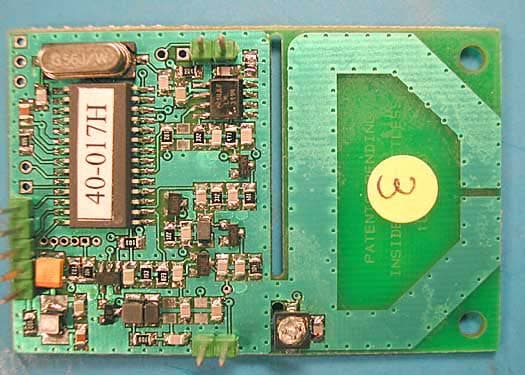
Click to zoom
Application Details
- Equipment Class
- DXX - Part 15 Low Power Communication Device Transmitter
- Date of Grant
- Jul 17, 2003
- Application Purpose
- Original Equipment
- Date of Application
- Jul 17, 2003
- Equipment Note
- Contactless Coupler, M210-2G
- Frequency Range
- 13.56000000 - 13.56000000
- Company
- Inside Secure
- Country
- France
Documents & Files
Document Text
Text extracted from the exhibit documents filed with the FCC. Open a document above to read the original.
Users Manual
M210-2G - Datasheet - M210-2G DS 1 Version 1.1 INSIDE CONTACTLESS M210-2G PROXIMITY READER 13.56 MHz for ISO chips - 14 443 type A and B - 15 693 - FeliCa DATASHEET Chips > Packaging > Readers > more... M210-2G - Datasheet - M210-2G DS 2 Version 1.1 Content CHAPTER 1 M210-2G DESCRIPTION FCC and CE compliance7 System Integration8 M210-2G dimensions and Pin Co-ordinates10 Mechanical Interface – Component View10 M210-2G Pin coordinates – Components View10 CHAPTER 2 M210-2G CONNECTION Power supply12 Characteristics12 Noise influence12 Serial Interface13 Character Format13 Baud rate13 ISO 7816 T=0 Interface14 M210-2G coupler Input and Outputs15 Input and Outputs characteristics15 Out2P power PIN15 How to reset M210-2G couplers16 Software reset16 Hardware reset16 M210-2G - Datasheet - M210-2G DS 3 Version 1.1 CHAPTER 3 COMMAND INTERFACE REFERENCE MANUAL HOST - COUPLER protocol2 description2 Block protocol4 Protocol configuration5 LRC5 Coupler commands overview7 SELECT_CARD8 SELECT_PAGE10 TRANSMIT12 GET_RESPONSE14 READ_STATUS15 SET_STATUS16 Modifiable parameters17 Coupler’s INPUTs AND OUTPUTS18 EEPROM free area18 DISABLE_COUPLER19 DISABLE_COUPLER ENHANCED20 ENABLE_COUPLER21 ASK_RANDOM22 LOAD_KEY_FILE23 SELECT_CURRENT_KEY24 DIVERSIFY_KEY25 GET_CONFIG26 M210-2G - Datasheet - M210-2G DS 4 Version 1.1 CHAPTER 4 USER’S GUIDE Managing INSIDE chips2 Security configuration3 Selecting a chip4 Selecting a page5 Reading chip memory6 Writing chip memory7 Halting a chip8 How to work with several chips in the field9 Managing INSIDE’s chips protocols10 Managing the security11 INSIDE chips security11 Key loading13 How to set a key as the active one14 How to authentify a chip15 How to authentify a PAGE15 Protecting the keys16 Managing STANDARD chips protocols17 Time out adjustment17 15 693-3 protocol17 ISO 14 443 type A18 ISO 14 443 type B18 FeliCa ( new version)18 Managing the RF field19 How to reset the RF field ?19 How to asleep the coupler19 How to wake up the coupler19 APPENDIX A HOW TO LOAD A KEY IN A COUPLER Exchange key21 General key loading procedure21 Terminology and notation22 Key loading step by step22 Algorithms23 Key permutation23 Checksum byte calculation23 Load key checksum calculation23 APPENDIX B ERROR CODE M210-2G - DATASHEET - M210-2G DS - 5 Version 1.1 Main Features : √√ √√ √Serial host interfaces: !ISO 7816-3 (T=0) compatible interface !RS-232 CMOS interface √√ √√ √ Security management: !Security module !Secure key loading √√ √√ √ Secured Key Storage √√ √√ √ Contactless interfaces: !ISO 15 693 !ISO 14 443 type A !ISO 14 443 type B !FELICA TM √√ √√ √Contactless transmission of data and energy supply √√ √√ √Carrier frequency: 13.56MHz √√ √√ √On board antenna √√ √√ √ Transparent mode for contactless data exchange √√ √√ √Supply voltage: 5V only √√ √√ √Low power consumption < 50 mA √√ √√ √Stand-by mode < 50 μA √√ √√ √Small PCB size: 61 x 41.5 mm √√ √√ √ Operating temperature range: -20°C to +50°C √√ √√ √Emission approval* : FCC, IDA singapore, Canadian, CE Product Ordering Code ProductOrdering codePackageTools Proximity Coupler M210-2GM210-2GPCB- * Note : The chassis will not allow ESD air discharge at voltage over 8 kV. The distance between the chassis and its packaging has to be superior to 0.68 mm. M210-2G - DATASHEET - M210-2G DS - 6 Version 1.1 CHAPTER 1 M210-2G DESCRIPTION M210-2G couplers are developed by INSIDE contactless for managing the RF communication interface with 13.56 MHz standard chips. They have the following features : "" "" "Operating frequency13.56MHz "" "" "Host interfaceRS-232 CMOS / ISO 7816 T=0* "" "" "Target applicationsProximity and short range applications "" "" "Target chipAll INSIDE’s chips, 15693 chips, 14443 chips (type A and type B), FELICA TM You will find in this chapter ... !! !! !two ways to build your application with INSIDE’s couplers !! !! !coupler’s mechanical characteristics (PIN position, size...) Afterwards, the term «coupler» stands for an electronic board that converts numeric commands into contactless chip commands using the RF interface. * Note : The host interface is not fully compliant with the ISO 7816 T=0 protocol. But all the coupler’s commands are builded on this format so that its integration in a device using this protocol is very easy. M210-2G - DATASHEET - M210-2G DS - 7 Version 1.1 FCC AND CE COMPLIANCE Federal Communications COMMISSION (FCC) Part 15 STATEMENT This equipment has been tested to FCC requirements and has been found acceptable for use. The FCC requires the following statement for your information: This equipment generates and uses radio frequency energy and if not installed and used properly, that is, in strict accordance with the manufacturer’s instructions, may cause interference to radio and television reception. It has been type tested and found to comply with the limits for a Class B computing device in accordance with the specifications in Part 15 of FCC Rules, which are designed to provide reasonable protection against such interference in a residential installation. However, there is no guarantee that interference will not occur in a particular installation. If this equipment does cause interference to radio or television reception, which can be determined by turning the equipment off and on, the user is encouraged to try to correct the interference by one or more of the following measures: ·If using an indoor antenna, have a quality outdoor antenna installed. ·Reorient the receiving antenna until interference is reduced or eliminated. ·Move the radio or television receiver away from the receiver/control. ·Move the antenna leads away from any wire runs to the receiver/control. ·Plug the receiver/control into a different outlet so that it and the radio or television receiver are on different branch circuits. This device complies with part 15 of the FCC rules. Operation is subject to the following two conditions : (1) this device may not cause harmful interference, and (2) : this device must accept any interference r…
Text truncated - open the document above for the full version.
Block Diagram
M210-2G BLOCK DIAGRAM Micr ocontr oller Data dec oding Carrier + data mixer (Amplifier) 13.56 MHz Crystal oscillator Carrier amplifier Antenna Coil trigger Band pass filter PCB Interface Connector Amplifier En vel o pe de tect or Line Dri ver RS T RX , TX Power Su ppl y Line VD C
Cover Letter(s)
INSIDE TECHNOLOGIES 11A, Parc Club du Golf 13856 Aix-en-Provence Cedex 3 - France Federal Communications Commission 7435 Oakland Mills Road Columbia, MD 21046 Gentlemen: This letter is to comply with Section 0.457(d)(2)(i) pertaining to confidential material. INSIDE TECHNOLOGIES would like the following documents regarding this submission for FCC ID Q45-M210-2G to be kept confidential. 1. Schematics, electronic file name “M210-2G_Schematics. PDF” The above material contains trade secrets or technical data, which would customarily be guarded from competitors. We do not want these documents to be accessible to the general public. Sincerely, INSIDE TECHNOLOGIES Mr Adel HAMZA Reader Operation Manager
External Photos
Top Bottom
ID Label/Location Info
Model: M210-2G This device may not cause harmful interference LISTED ACCESSORY C ! Complies with IDA Standards DA102907 Canada 210 Electrical Rating: 5.0V " 45mA Made in France 0.7" 0.9" FCC ID: Q45M210
Internal Photos
Top with Antenna (on the right) Top Close Up 1 Top Close Up 2 Top Close Up 3 Antenna Top Close Up 1 Antenna Top Close Up 2 Bottom Bottom Close Up 1 Bottom Close Up 2 Antenna Bottom Close Up 1 Antenna Bottom Close Up 2 Side 1 Side 2 (on stand for photo) Side 3 Side 4 EUT on Development Board (without antenna)
Operational Description
M210-2G Theory of Operation In the communication protocol, the data send by the reader to the chip is mixed with the 13.56MHz carrier, amplified and sent to the antenna coil. An ASK signal coming from the chip is recognized by the reader as an amplitude modulation of the carrier signal. The reader needs two steps for a full recovery of the data. The first step is demodulating the backscattering signal, and the second step is to adapt the level to the microcontroller that performs the signal decoding. The demodulation is accomplished by detecting the envelope of the carrier signal. A half- wave capacitor-filtered rectifier circuit is used for the demodulation process. A diode detects the peak voltage of the backscattering signal. The demodulated signal must then pass through band pass filter, amplifier and trigger (signal shaping) circuit before it is fed to the microcontroller. The microcontroller performs data decoding and an asynchronous serial data stream utilizing an open-collector interface.
Test Report
Page 1 of 45 Report No.: FC03-038 INSIDE TECHNOLOGIES TEST REPORT FOR THE CONTACTLESS COUPLER, M210-2G FCC PART 15 SUBPART C SECTIONS 15.207, 15.209 & 15.225 COMPLIANCE DATE OF ISSUE: JUNE 20, 2003 PREPARED FOR: Inside Technologies MS: Bat 11A, Parc Club du Golf ZAC de la Pichaury 13856 Aix En Provence, France PREPARED BY: Joyce Walker CKC Laboratories, Inc. 5473A Clouds Rest Mariposa, CA 95338 W.O. No.: 80687 Date of test: June 16-18, 2003 Report No.: FC03-038 This report contains a total of 45 pages and may be reproduced in full only. Partial reproduction may only be done with the written consent of CKC Laboratories, Inc. The results in this report apply only to the items tested, as identified herein. Page 2 of 45 Report No.: FC03-038 TABLE OF CONTENTS Administrative Information ............................................................................................. 4 Summary of Results......................................................................................................... 5 Conditions for Compliance.............................................................................................. 5 Approvals......................................................................................................................... 5 FCC 15.31(e) Voltage Variation ..................................................................................... 6 FCC 15.31(m) Number of Channels................................................................................ 6 FCC 15.33(a) Frequency Ranges Tested ......................................................................... 6 FCC 15.35 Analyzer Bandwidth Settings........................................................................ 6 FCC 15.203 Antenna Requirements ................................................................................ 6 FCC 15.205 Restricted Bands ......................................................................................... 6 Mode of Operation........................................................................................................... 7 EUT Operating Frequency............................................................................................... 7 Temperature and Humidity During Testing .................................................................... 7 Equipment Under Test (EUT) Description...................................................................... 7 Equipment Under Test..................................................................................................... 7 Peripheral Devices ........................................................................................................... 7 Report of Measurements.................................................................................................. 8 Table 1: FCC 15.207 - Six Highest Conducted Emission Levels ...................... 8 Table 2: FCC 15.209 - Six Highest Radiated Emission Levels.......................... 9 Table 3: FCC 15.225(a) - Fundamental Emission Levels .................................. 10 Table 4: FCC 15.225(b) - Six Highest Radiated Emission Levels ..................... 11 FCC 15.255(b)/ 15.215 - Bandedge Compliance ................................................ 12 FCC 15.255(b)/ 15.215 - Bandedge Compliance ................................................ 13 FCC 15.225(c) – Frequency Tolerance, Voltage and Temperature .................... 14 RSS 210 6.2.2(e) – 99 % Bandwidth................................................................... 15 RSS 210 6.2.2(e) – Emissions Mask ................................................................... 16 EUT Setup .......................................................................................................................17 Correction Factors ........................................................................................................... 17 Table A: Sample Calculations ............................................................................. 17 Test Instrumentation and Analyzer Settings.................................................................... 18 Spectrum Analyzer Detector Functions............................................................... 18 Peak ......................................................................................................... 18 Quasi-Peak............................................................................................... 18 Average.................................................................................................... 18 EUT Testing ....................................................................................................................19 Mains Conducted Emissions ............................................................................... 19 Radiated Emissions ............................................................................................. 19 Appendix A: Test Setup Photographs ............................................................................. 20 Photograph Showing Mains Conducted Emissions............................................. 21 Photograph Showing Mains Conducted Emissions............................................. 22 Photograph Showing Radiated Emissions ........................................................... 23 Page 3 of 45 Report No.: FC03-038 Photograph Showing Radiated Emissions ........................................................... 24 Photograph Showing Radiated Emissions ........................................................... 25 Photograph Showing Radiated Emissions ........................................................... 26 Photograph Showing Radiated Emissions ........................................................... 27 Photograph Showing Temperature Testing ......................................................... 28 Appendix B: Test Equipment List ................................................................................... 29 Appendix C: Measu…
Text truncated - open the document above for the full version.
Test Setup Photos
PHOTOGRAPH SHOWING MAINS CONDUCTED EMISSIONS Mains Conducted Emissions - Front View PHOTOGRAPH SHOWING MAINS CONDUCTED EMISSIONS Mains Conducted Emissions - Side View PHOTOGRAPH SHOWING RADIATED EMISSIONS Radiated Emissions - Front View PHOTOGRAPH SHOWING RADIATED EMISSIONS Radiated Emissions - Front View PHOTOGRAPH SHOWING RADIATED EMISSIONS Radiated Emissions – Close-up View PHOTOGRAPH SHOWING RADIATED EMISSIONS Radiated Emissions - Showing Loop Antenna PHOTOGRAPH SHOWING RADIATED EMISSIONS Radiated Emissions - Showing Log Antenna PHOTOGRAPH SHOWING TEMPERATURE TESTING Temperature Testing - Front View With Door Closed
Contact Information
Applicant
Serge Demange(Hardware Operation Manager)
Technical Contact
CKC Laboratories, IncMary Ellen Clayton
[email protected]209-966-5240
5473A Clouds Rest · Mariposa, California · United States
Non-Technical Contact
CKc Laboratories, IncMary Ellen Clayton
[email protected]209-966-5240
Test Firm
CKC Laboratories, Inc.Steve Behm
Technical Specifications
| # | Rule Parts | Frequency Range | Power Output |
|---|---|---|---|
| 1 | 15C | 13.56 MHz - 13.56 MHz | - |
Other Applications from Inside Secure
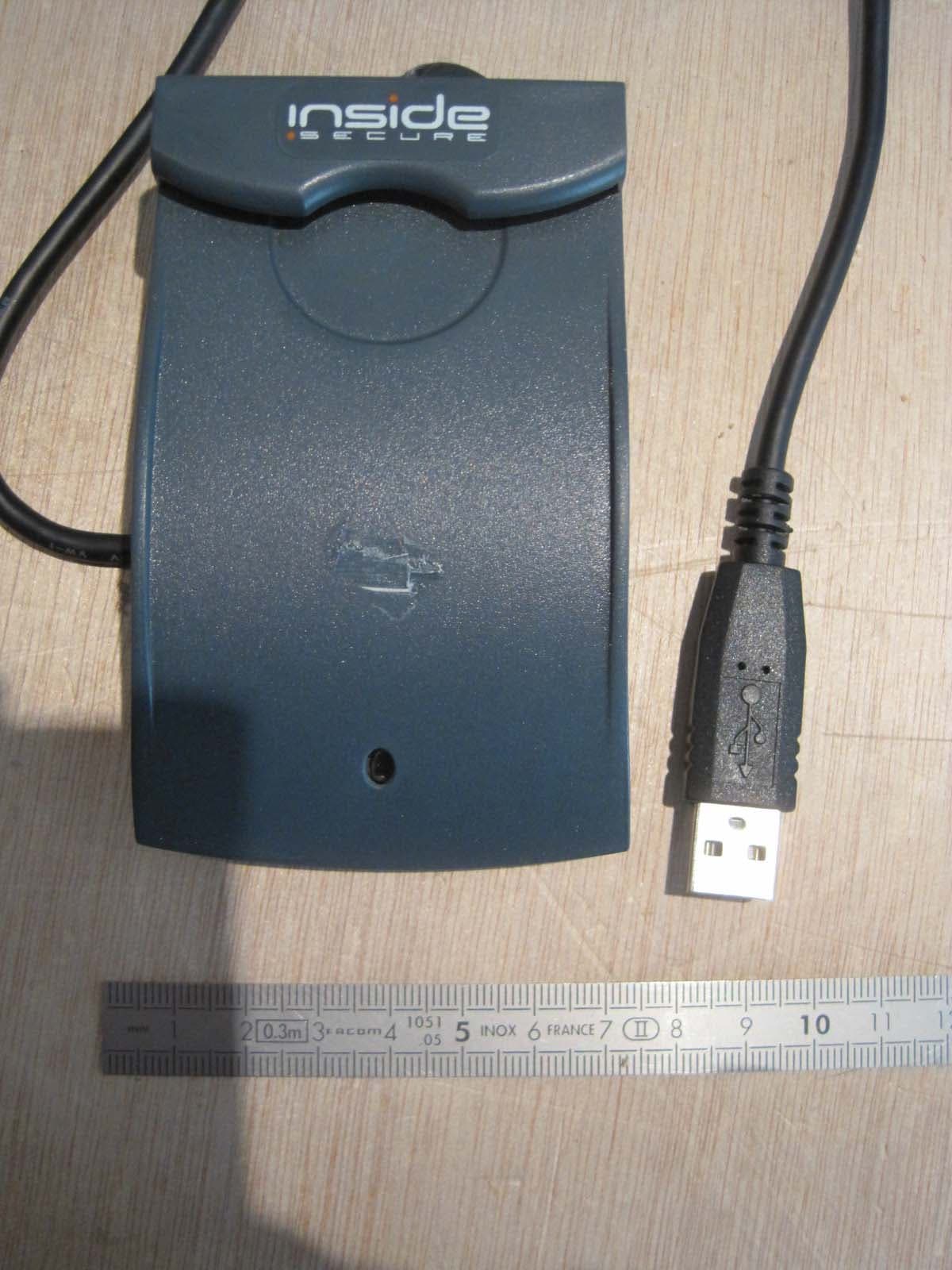
Q45DESKREAD
Jul 09, 2012TAG READER
Equipment Class
DXX - Part 15 Low Power Communication Device Transmitter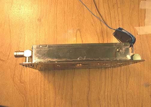
Q45M300
Apr 11, 2005Radio Frequency Transceiver
Equipment Class
DXT - Part 15 Low Power Transceiver, Rx Verified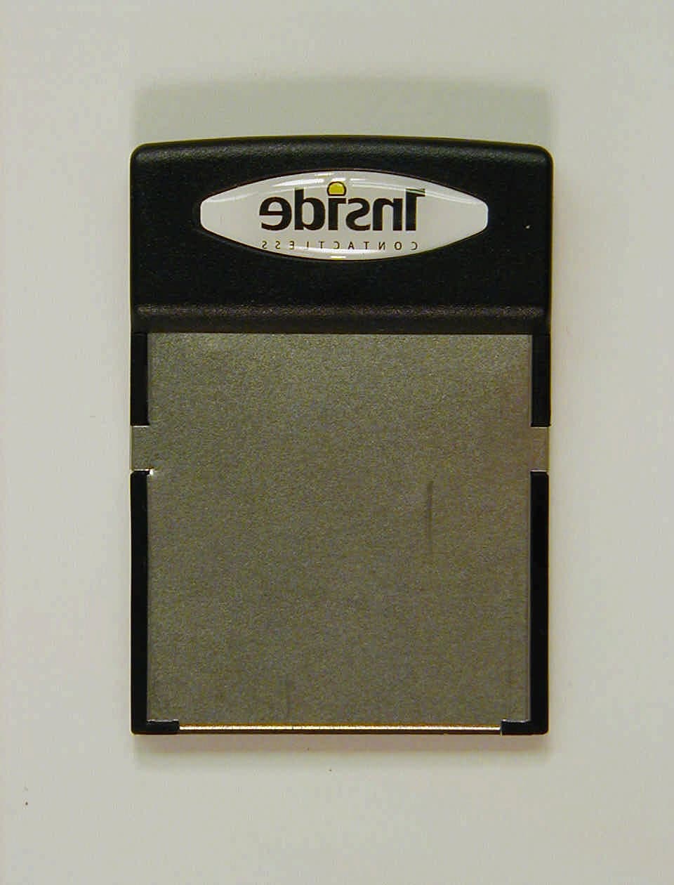
Q45M2502G
Mar 24, 2004Hand'it - 2G CF RFID Reader
Equipment Class
DXT - Part 15 Low Power Transceiver, Rx Verified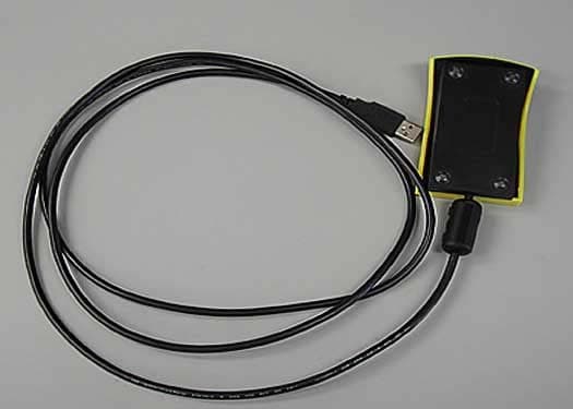
Q45ACCESSO
Oct 21, 2003Desktop Reader
Equipment Class
DXT - Part 15 Low Power Transceiver, Rx Verified