Q5EPT420001Two Way Radio
Kirisun Communication Co., Ltd.
Click to zoom
Application Details
- Equipment Class
- TNF - Licensed Non-Broadcast Transmitter Held to Face
- Date of Grant
- Aug 09, 2006
- Application Purpose
- Original Equipment
- Date of Application
- Aug 09, 2006
- Equipment Note
- Two Way Radio
- Frequency Range
- 421.00000000 - 470.00000000
- Country
- China
Documents & Files
Document Text
Text extracted from the exhibit documents filed with the FCC. Open a document above to read the original.
Users Manual
FM HANDHELD TRANSCEIVER INSTRUCTION MANUAL PT4200-01 We are very grateful for your purchasing brand two- way radios produced by Kirisun Electronics (Shenzhen) Co., Ltd. We believe two-way radio, which always incorporates the latest technology, can bring great convenience to your life and work; we also believe that the quality and function of two- way radio can meet your demands for reliable communication. PRECAUTIONSPlease observe the following precautions to prevent fire, personal injury, and radio damage. Do not operate your radio while taking on fuel, or being charged. Do not expose the radio for a long period to direct sunlight, nor place the radio close to heating appliances. Do not place the radio in excessively dusty areas, humid INSTRUCTION MANUAL FM HANDHELD TRANSCEIVER NOTE 17 PT4200-01 areas or on unstable surfaces. Do not modify this radio for any reason. Refer service to qualified licensed or certificated technicians only. Notice to the User: Government laws prohibit radio communication without permission in government districts. Illegal operation is subject to punishment by fine and/or imprisonment. Refer service to the well-trained professional technicians only. SafetyIt is important that the user is aware of and understands hazards common to the operation of any radios.Warning!Turn off your radio before entering any area with a potentially explosive atmosphere (where the air contains gas, dust and smog, etc.), such as while taking on fuel, or while parking at a gasoline service station.Precautions in UsePlease comply with the following attentions to avoid fire, bodily injury and damage to the radio. The radio is recommended to transmit for 1 minute and receive for 4 minutes. Long time transmitting or continuous working in high power mode will make the rear side of the radio generate heat. Please don't disassemble or assemble the radio under any circumstances. Please don't expose the radio to direct sunlight for a long time; don't place the radio near any heating devices, either. Please don't put the radio in extremely dusty, moist or dabbling places; don't place it on any unstable surfaces, either. If the radio emits smoke or strange odors, turn it off and remove the battery from the radio and promptly contact your local authorized Kirisun dealer. CONTENTSUNPACKING AND CHECKING ..............................1 SUPPLIED ACCESSORIES .........................................................1 PREPARATION ..............................................................................2 CHARGING THE BATTERY PACK ... ...........................................2 INSTALLING/REMOVING THE BATTERY PACK ..........................3 INSTALLING THE ANTENNA ........................................................4 INSTALLING THE OPTIONAL SPEAKER/MICROPHONE ...........4 INSTALLING/REMOVING THE BELT CLIP ...................................4 RADIO OVERVIEW ........................................................................5 BASIC OPERATION ......................................................................6 SCAN FUNCTION ..........................................................................7 STARTING SCAN ...........................................................................7 STOPPING SCAN ......................................................................7 AUXILIARY FUNCTIONS ............................................................10 TIME-OUT TIMER ........................................................................10 BATTERY SAVING .......................................................................10 LOW BATTERY WARNING ..........................................................10 MONITOR ..................................................................................10 CTCSS/DCS ................................................................................11 VOICE ANNUNCIATION OF CURRENT CHANNEL NUMBER ..11 WIRED CLONE .............................................................................12 EMERGENCY ALERT ...................................................................13 TROUBLESHOOTING GUIDE ....................................................14 STTINGS .....................................................................................15 EQUIPMENT ITEM QUANTITY 1111111 UNPACKING AND CHECKING EQUIPMENT Carefully unpack the radio. We recommend that you identify the items listed in the following table before dis-carding the packing material. If any damage has occurred during shipment,please contact the dealer immediately . SUPPLIED ACCESSORIES Hand strap Belt clip Li-ion battery pack Charger Power adapter Instruction manual Belt clip Charger Battery Antenna 2 Antenna PREPARATION CHARGING THE BATTERY PACK * * Notice: A new battery or a battery whose power appears low (power indicator displays one bar or no bar) needs charging before using. The battery is not fully charged in the factory, and probably the new battery is falsely indicated as full charge. Before the initial use, please charge the new battery. Kirisun KB-58L Li-ion battery is supplied. When charge the battery for the first time after purchase or long-time storage (over 2 months), please repeat charging several times to 1) Plug the adapter into an AC wall outlet; connect the power adapter with the battery charger, and then the indicator lights yellow.2) Place the battery or radio into the charger slot. Make sure the battery is well connected with the charger. The indicator turns red, and then the charger gets in the state of charging automatically. Charging time is about 5 hours. When battery is fully charged the indicator turns green.While in green light state, keep the battery remain in the charger for 1~2 hours, which will give you the best battery performance. And then disconnect the adapter from the AC outlet. * 1 Hand Strap Power Adapter INSTALLING /REMOVING THE BATTERY PACK 4 3 * resume the battery normal capacity. Do not charge the battery again if it has been fully charged or …
Text truncated - open the document above for the full version.
Users Manual
BASIC OPERATION 6 5 LED Indicator Lights red while transmitting; lights green while receiving a signal.Flashes red while in low battery power. Channel Selector Rotate to select channel 1-16. Power/Volume Switch Turn clockwise to switch on the radio. Turn counterclockwise till a click is heard to switch off the radio.Rotate it to adjust the volume after turning on the radio. PTT (Push-to-talk) To make a call, press and hold the PTT button, then speak into the microphone in normal voice. Release the PTT button to receive a call. Monitor Button Press to disable the SQUELCH, and enable the SQUELCH again. Channel Annunciation Button Press it in standby state, and the channel number will be annunciated. If press and hold this button, and at the same time switch on the radio again, the type of voice annunciation of 1 2 3 4 5 6 7 8 channel number will be changed. Emergency Button Press and hold this button for over 2 seconds to activate warning tone. Press it again to exit the emergency alert state. Note:When warning tone sounds, all of the buttons are disabled. Microphone/Speaker Jacks For connecting external Microphone/Speaker. Switch On Switch on the radio by turning the Power/Volume switch clockwise till a click is heard, then the radio will be in the state of stand by and you will hear a beep if the dealer has set it. And then you will hear voice annunciation of the current channel number.Adjust Volume Press the monitor button to listen to the background noise and rotate the Power/Volume switch to adjust volume.Select Channels Rotate the channel selector to select channels. You will hear voice from the speaker while receiving proper signals.If voice annunciation of channel number has been set, the radio will annunciate the current channel number. RADIO OVERVIEW 8 7 Make a Call To make a call, select the desired channel, press and hold the PTT button, and speak in normal voice. Please keep your mouth 3~8 cm away from the microphone. Receive a Call Release the PTT button to receive a call. Select the desired channel, adjust the volume to a proper level, and then you can receive others' voice. (Your local dealer may prohibit this function.)Only when there are no less than two channels added in the scan list and the scan function has been activated, the radio can start scanning. STARTING SCANWhen switching to channel 16, the radio will begin to scan, and pause after receiving signals. STOPPING SCANWhen switching to channel 1-15, the radio will stop scanning.Introduction:1. Dealer can set the following two ways to restart scanning after its pause: 1) Time-control The radio will restart scanning after pausing for some time while receiving signals. The pausing time can be preset from 0.5 to 5 seconds. 2) Carrier wave control The radio will pause scanning after receiving signals and will restart scanning 3 seconds after the signal disappears.2. The working channel of the radio will respond to the following channels automatically when pressing PTT button during scanning. The dealer can select one among the following six ways. 1) Last called When pressing PTT button, the radio will transmit from the last channel that received a call.2) Last used + currently working channel When pressing PTT button during the scanning, the radio will transmit from the last channel that received a call. When pressing PTT button during the scanning pause, the radio will transmit from the currently working channel. 3) Selected channel When pressing PTT button, the radio will transmit from the first channel of the scanning list. 4) Selected channel + currently working channel When pressing PTT button during scanning, the radio will always transmit from the first channel in the scanning list. When pressing PTT button during the scanning pause, the radio will always transmit from the currently working channel. 5) Priority channel The radio will transmit signals from the priority channel in the scan list when pressing PTT button. 6) Priority channel + currently working channel When pressing PTT button during scanning, the radio will always transmit from the priority channel. When pressing PTT button during SCAN FUNCTION AUXILIARY FUNCTIONS 10 9 the scanning pause, the radio will transmit from the currently working channel.Note: Currently working channel means the channel in which the radio holds on under the following four conditions.1) After receiving the signals, the radio will still stay in the current channel before restarting the scan. 2) When receiving signals during scanning, the radio will pause on the current channel and will keep staying on it for 3 seconds after the signals disappear.3) Radio will stay on the current channel when pressing PTT during scanning.4) When the radio transmitting ends by releasing PTT button, within the transmitting pause time preset by the local dealer, the radio will stay in the current channel. Selected channel: The first channel in the scanning list set by the dealer. Priority channel: The prior channel in the scanning list set by the dealer. Only when priority channel has been selected, the options of priority channel and priority channel + currently working channel in Revert Channel are available. TIME-OUT TIMER Time-out timer can prevent the user from continuously talking overlong and prevent the radio body heating due to continuous longtime transmitting.If you continuously transmit longer than the time limit preset by the dealer, the radio will stop transmitting and warning tone sounds, and to stop the warning tone please release the PTT button. Pressing the PTT button again will resume transmitting. BATTERY SAVING The automatic battery saving function decreases the power consumption when no signal is received and no operation is conducted.If the battery saving function is activated, 10 seconds after the radio doesn't receive any signals or no operation is being conducted, the radio enters battery saving mode. When a signal is received or any operation occurs, it exits battery sav…
Text truncated - open the document above for the full version.
External Photos
EXHIBIT B - EUT PHOTOGRAPHS EUT – Front View EUT – Back View
ID Label/Location Info
EXHIBIT A - FCC ID LABELING AND LOCATION Proposed FCC ID Labeling Proposed FCC ID Location FCC ID Label Location ATTENTION! Restricted to occupational use to satisfy FCC RF exposure limits. See users manual for operating requirements. FCC ID: Q5EPT420001 Model: PT4200-01
Internal Photos
EXHIBIT C - EUT INTERNAL PHOTOGRAPHS EUT – Inside View (1) EUT –Inside View (2) Battery View (1) Battery View (2) ANT View EUT –PCB Front View EUT –PCB Back View
Operational Description
Circuit Description 1. Frequency Configuration Figure1 Frequency Configuration This radio adopts the 2 nd Mixer, the 1 st IF 49.95MHz, the 2 nd IF 450kHz. The receiver’s first local oscillation is generated by the frequency synthesizer. The second local oscillation is generated by the crystal oscillator. The transmitter signals are generated by frequency synthesizer. The reference frequency of frequency synthesizer is generated by TCXO. 2. Receiver (RX) BPFBPF Q20Q19 Q21 VCO XF1 IF SYSTEM CF1 IC8IC6C IC6A,B,D NOISE AMP NOISE DETECT MCU CTCSS/DCS Filter MCU IC4 Q7 D17,D18 MCU SQ CONTR VOICE VOICE SW ALARM/Beep Q9 IC13 Q24 Figure 2 Receiver Illustration The Receiver Front Terminal Signals from the antenna pass through the RX/TX switch (D1, D2, D4, D5); and then undesirable out-of-band signals will be filtered out at the band pass filter (BPF) consisting of C227, L8, L15, C70, C126, C218, L9, C217, L10, C127; then signals are amplified at the low noise amplifier (LNA) consisting of Q20 and its peripheral components. The output from the LNA passes the BPF consisting of L5, L6, L7, C228, C124, and C132 for filtering and then is sent to the first grade frequency mixer (Q19). TX/RX SW MIC SP Audio Amp CF1 450kHz 20.95MHz X3 IF SYSTEM XF1£¬XF2 21.4MHz TCXO X4 13MHz VCO IC8 300--3000Hz 300--3000Hz Mic Amp MCU produces output voltages and alters the capacitance of the variable capacitor diodes D21, D22, D23, D24, D26, D30 to control the center frequency of the band-pass filter. The First Frequency Mixer After mixing the receiving signals and the first local oscillation signals from the frequency synthesizer, the 1 st IF signals (49.95MHz)are generated. The first IF signals pass the crystal filter (XF1, XF2) , which will filter the signals of adjacent channel and those out of band. IF Circuit The 1 st IF signals from the crystal filter are amplified at the first IF amplifier (Q21), and then are sent to the IF processing IC (IC5, MC3361). The IF IC consists of the 2 nd frequency mixer, the 2 nd local oscillator, IF amplifier, limiter, phase frequency detector, and noise amplifier. IC5 inner circuit and X3 (49.5MHz) compose the 2 nd local oscillator. The 2 nd local oscillation (49.5MHz) and the 1 st IF signal (49.95MHz) are mixed at IC5 to generate the 2 nd IF(450MHz). After the 2 nd IF signal is amplified and its amplitude is limited at IC5, and then filtered at porcelain filter (CF1,450kHz), IC5 demodulates and sends out audio signals. CD1 FM Demodulator Limiter Amp OSC Amp Filter Noise Amp AF out IF in CF1 450kHz 21.4MHz X3 20.95MHz Figure 3 IF System Receiver Audio Signal Processing IC6 and its peripheral circuit compose the receiver audio signal processing circuit. IC5 sends audio signals to IC6-C for amplification, and then to IC4 (CTCSS signaling filtering circuit) and IC6-D. After the signals are amplified, de-emphasized, filtered at IC6 and other cells, the HF (high frequency) and LF (low frequency) will be eliminated, and the remaining 300-3000Hz audio is sent to Q9 for amplification and then to volume potentiometer for adjustment and finally sent to the audio amplifier (IC8). C226 R58 IC4A IC4B LPF,Amp LPF,Amp LPF,AmpLPF,Amp HPF,Amp IC6C IC6D IC6AIC6B Q9 Q24 CTCSS/DCS AF out SQ from MCU to MCU Figure 4 Receiver Audio Processing Squelch Circuit Demodulation output from IC5 is sent to the selection frequency noise amplifier, which consists of IC5 inner noise amplifier and C107, R124, R152, C33, and C35, to be filtered off the noise. After being amplified at Q7, noise is sent to D17 and D18 for wave checking and then sent to MCU, which determines the noise volume to control the squelch. Audio Amplifier IC8 and peripheral components construct the audio amplifier. Receiving audio signals, voice indication signals, indication tone signals and warning tone signals are collected for audio amplification to drive the speaker. Warning tone has no volume control. When AFCO is at the high level, Q37, Q8, Q33, and Q38 will be connected, and IC8 starts working and voice comes out from the speaker. Q36: Receiving audio signal switch Q35: Warning tone switch Q25: Indication tone switch CTCSS Signal Filtering The IC5 demodulated output audio signals may contain CTCSS (continuous tone coded squelch system) and DCS (digital coded squelch). The frequency spectrum of CTCSS/DCS is 2-250Hz. The filtering circuit constructed by IC4 can filter out the signals out of the CTCSS/DCS frequency spectrum to ensure MCU to decode CTCSS/DCS more precisely. 3. Transmitter (TX) Transmitter Amplifier to RX to ANT 5T Q2Q3Q12Q11 2SC5018 2SC3356 RD01MUS1RD07MVS1 LPF ANT SW BATTARY APC VCO Figure 5 Amplifier and Antenna Switch Diagram The modulated signals from VCO are amplified at Q2, Q3, and Q12 and then are sent to Q11 for amplification. Q11 output power: 4.5W. The Q11 and Q12 gate offset is controlled by APC circuit. Changing gate-offset voltage can control the transmitter output power conveniently. APC (Auto Power Control) R167R168 R169 IC3A IC3B Q17 to Q11(G),Q12(G) to MCU to Q11,Q12 BATTARY Figure 6 APC Circuit R167, R168, and R169 are the amplifier current checker; IC3A is the sample amplifier of the amplification current; IC3B is the power comparison amplifier. If the transmitter output power is too big, the amplifier current will increase, IC3A output will mount, IC3B output voltage decrease, the offset voltage added to Q11 and Q12 will decrease, and then the transmitter output power will decrease. Vice versa, such can ensure steady transmitter output power in different working circumstances. MCU changes the input power to IC3B to set the power. Transmitter Audio Signal Processing TCXO VCO MCU CTCSS/DCS MIC MIC Amp Pre-Emphasis IC7A IC7B IC7C,IC7D Figure 7 Transmitter Audio Circuit IC7 and the peripherals components construct the transmitter audio processing circuit. After the audio signals from MIC are amplified, the amplitude of them is limited, and are filtered, they are sent to VCO together with CTCSS/DCS for modulat…
Text truncated - open the document above for the full version.
Parts List/Tune Up Info
NO. Description Ref.No 1 PCB,PT558N-06022 8 2 IC,PST9140NRIC11 3 KIA6278F,AUDIO,AM PIC8 4 IC,AT24C08N-10SI2. 7IC9 5 PLL IC,MB15E03SL,PLL,16-PIN,SSO PIC1 6 IC,HT7130-1,SOT-8 9IC14 7 IC,HT7150-1IC12 8 NJM2902V,OP-AM PIC4,IC6,IC7 9 NJM2904V,OP-AMPIC3 10 MCU,M38034M4H-284H PIC10 11 IC,MC3361B PIC5 12 DIODE,MA77,080 5D1 13 DIODE,0805,MA360(PANASONIC)D12 14 DIODE,1SS372(TOSHIBA)D13 15 DIODE,0603,MA2S111(PANASONIC)D15,D16,D2 5 16 DIODE,DAN222,(ROHM)D308 17 DIODE,HSC277(HITACHI)D3,D4,D6,D 7 18 DIODE,0603,HVC350B(HITACHI)D21,D22,D23,D24,D26,D30 19 DIODE,HVC376BD8,D9,D10,D11 20 DIODE,HZU5ALL(HITACHI)D14 21 DIODE,IN414 8D17,D18 22 DIODE,0603,绿色,H19-21SYGCD20,D29 23 DIODE,0603,红色,19-21SURC/S530-A2/TR8D28 24 DIGITAL TRANSISTOR,DTA144EE(ROHM)Q17,Q3 4 25 DIGITAL TRANSISTOR,DTC144EE(ROHM)Q22,Q23,Q26,Q27,Q33,Q37 26 DIGITAL TRANSISTOR,KRX102U,with,bias,resistor, IC2 27 DIGITAL TRANSISTOR,FMMT717T AQ8,Q30 28 DIGITAL TRANSISTOR,2SC162 3Q10 29 DIGITAL TRANSISTOR,2SC335 6Q3 30 DIGITAL TRANSISTOR,2SC4617(S)(ROHM )Q6,Q9 31 DIGITAL TRANSISTOR,2SC4738(GR),AF,AMPLIFIER(TOSHIBA) Q7 32 DIGITAL TRANSISTOR,2SC4919,MUTING,CIRCUIT(SANYO ) Q24 33 DIGITAL TRANSISTOR,2SC5108Y(TOSHIBA )Q2,Q4,Q5 34 DIGITAL TRANSISTOR,KTA1298(Y)Q29,Q31,Q3 2 35 DIGITAL TRANSISTOR,KTC4082,(KEC)Q21 36 DIGITAL TRANSISTOR,2SJ24 3Q16 37 DIGITAL TRANSISTOR,2SK508NV(K52)Q14,Q15 38 DIGITAL TRANSISTOR,3SK31 8Q19,Q20 39 DIGITAL TRANSISTOR,RD01MUS 2Q12 40 DIGITAL TRANSISTOR,RD07MVS 1Q11 41 DIGITAL TRANSISTOR,2SK1588(NEC)Q38 42 DIGITAL TRANSISTOR,2SK182 4Q13,Q25,Q35,Q36 43 SWITCH,SKHLLBA010K1 44 SWITCH,4.5*4.5*4. 8K2,K4 45 SWITCH,SKRTLBE01 0K3 46 SWITCH,RD835E-GA1-16C-0F0 1SW2 47 JTBM455C2 4L57 48 LTM450HT,450kHz±3kH zCF1 49 49.95MHz±7.5KHz,U-5* 2XF1,XF2 50 CHIP R,0402,0R±5% C67,C166,C247,C276,C277,R4,R24,R30,R99,R15 4,R174,R217,R255,R260,R26 1 51 CHIP R,0402,10R±5%R98,R127,R200,R238 PT4200-01 PARTS LIST NO. Description Ref.No PT4200-01 PARTS LIST 52 CHIP R,0402,100R±5%R12,R94,R128,R237 53 CHIP R,0402,1K±5% R29,R39,R41,R42,R48,R49,R50,R111,R129,R130 ,R131,R157,R184,R195,R199,R27 3 54 CHIP R,0402,10K±5% R109,R120,R121,R122,R123,R126,R133,R140,R1 94,R205,R206,R212,R228,R254,R264,R266,R268 ,R295 55 CHIP R,0402,100K±5 %R105,R108,R113,R114,R115,R116 56 CHIP R,0402,1M±5%R160,R162 57 CHIP R,0402,1.2K±5 %R188 58 CHIP R,0402,12K±5 %R208 59 CHIP R,0402,120K±5 %R6,R7,R8,R9 60 CHIP R,0402,15K±5%C187,C188,C189,C265,R64,R76,R142,R192 61 CHIP R,0402,150K±5%R201 62 CHIP R,0402,1.8K±5 %R224 63 CHIP R,0402,18K±5 %R218,R219 64 CHIP R,0402,180K±5%R67 65 CHIP R,0402,20K±5% R27,R207,R225,R226,R227,R240,R263,R265,R26 7,R269 66 CHIP R,0402,220R±5 %R214,R215,R216 67 CHIP R,0402,2.2K±5%R294 68 CHIP R,0402,22K±5 %R209,R210,R211 69 CHIP R,0402,220K±5 %R86,R87,R164 70 CHIP R,0402,2.7K±5%R223 71 CHIP R,0402,27K±5 %R46,R171,R172,R257 72 CHIP R,0402,270K±5%R231 73 CHIP R,0402,3.3K±5 %R59,R60 74 CHIP R,0402,33K±5 %R196,R258,R290 75 CHIP R,0402,330K±5%R82 76 CHIP R,0402,3.9K±5 %R221,R222 77 CHIP R,0402,39K±5 %R53,R149,R153 78 CHIP R,0402,390K±5%R165 79 CHIP R,0402,470R±5 %R3 80 CHIP R,0402,4.7K±5 %R118,R125,R155,R156,R204,R248 81 CHIP R,0402,47K±5%R17,R18,R19,R20,R21,R22,R292 82 CHIP R,0402,470K±5%R166,R232,R293 83 CHIP R,0402,5.6K±5%R63,R65,R132 84 CHIP R,0402,56K±5%R173,R175,R176,R177,R178,R291 85 CHIP R,0402,560K±5%R163 86 CHIP R,0402,6.8K±5 %R220 87 CHIP R,0402,68K±5 %R78,R245 88 CHIP R,0402,820R±5 %R33 89 CHIP R,0402,8.2K±5 %R229,R230 90 CHIP R,0402,82K±5%R52 91 CHIP R,0402,91K±5 %R77,R213 92 CHIP R,0603,0R±5% C1,C86,C266,C273,L16,L34,L42,L62,R23,R28,R 81,R141,R182,R241,R26 2 93 CHIP R,0603,10R±5%R95,R96,R97,R101 94 CHIP R,0603,100R±5 %R74,R88,R89,R90,R180 95 CHIP R,0603,1K±5%R37,R38,R47,R150,R234,R256 96 CHIP R,0603,10K±5% R92,R117,R119,R124,R136,R137,R138,R139,R20 3 97 CHIP R,0603,100K±5% R43,R79,R80,R84,R102,R103,R104,R107,R158,R 197,R235,R243,R247,R249,R29 7 98 CHIP R,0603,1.2K±5%R69 99 CHIP R,0603,120K±5 %R5,R66 100 CHIP R,0603,15R±5 %R31 NO. Description Ref.No PT4200-01 PARTS LIST 101 CHIP R,0603,150R±5%R179 102 CHIP R,0603,1.5K±5 %R54 103 CHIP R,0603,15K±5 %R75 104 CHIP R,0603,150K±1 %R143,R144,R145,R146,R147,R170 105 CHIP R,0603,180R±5%R70,R71,R91,R189 106 CHIP R,0603,22R±5%L54,R93 107 CHIP R,0603,2.2K±5 %R2,R185,R186,R187 108 CHIP R,0603,220K±5%R233 109 CHIP R,0603,270R±5 %R34,R35 110 CHIP R,0603,2.7K±5 %R40 111 CHIP R,0603,270K±5 %R85 112 CHIP R,0603,33R±5 %R72 113 CHIP R,0603,3.3K±5 %R55,R56,R57,R58 114 CHIP R,0603,39K±5%R68,R193 115 CHIP R,0603,47R±5 %R15,R32 116 CHIP R,0603,470R±5 %R25 117 CHIP R,0603,4.7K±5 %R151,R152,R159,R183 118 CHIP R,0603,47K±5%R10,R11,R13,R14 119 CHIP R,0603,560R±5%R202,R244 120 CHIP R,0603,5.6K±5%R44,R61,R62,R191 121 CHIP R,0603,56K±5 %R16,R239 122 CHIP R,0603,560K±5 %R148 123 CHIP R,0603,68R±5 %R73 124 CHIP R,0603,68K±5 %R190 125 CHIP R,0603,8.2K±5 %R36 126 CHIP R,0603,82K±5 %R51 127 CHIP R,0805,0R±5 %L63 128 CHIP R,1206,0.47R±5 %R167,R168,R169 129 CHIP R,MVR22HXBRN473,47K±25%,B LinearVR2 130 CHIP R,MVR22HXBRN683,68K±25%,B Linea rVR1 131 SWITCH,RD810S-JA1-A103-0C6 1SW1 132 CHIP C,0402,10P±0.5P,50V,C0 GC257 133 CHIP C,0402,100P±5%,50V,C0 GC171,C196 134 CHIP C,0402,1000P±10%,50V,X7RC75,C105,C106,C110,C111,C263,C278,C310 135 CHIP C,0402,0.01uF±10%,50V,X7RC50,C149,C155,C159,C160,C161,C162,C279 136 CHIP C,0402,0.1uF,+80%--20%,16V,Y5V C85,C101,C167,C168,C173,C176,C177,C178,C27 1,C286 137 CHIP C,0402,0.1uF±10%,16V,X7 RC307 138 CHIP C,0402,1uF±10%,50V,X7 RC170,C235,C252,C303 139 CHIP C,0402,1500P±10%,50V,X7RC289 140 CHIP C,0402,0.018uF±10%,50V,X7 RC156 141 CHIP C,0402,2200P±10%,50V,X7 RC215 142 CHIP C,0402,0.022uF±10%,50V,X7 RC242,C243,C245 143 CHIP C,0402,0.027uF±10%,50V,X7RC179,C185 144 CHIP C,0402,3300P±10%,50V,X7 RC113 145 CHIP C,0402,0.033uF±10%,16V,X7 RC224,C244 146 CHIP C,0402,3900P±10%,50V,X7RC82,C222,C238,C284 147 CHIP C,0402,0.039uF±10%,50V,X7RC223 148 CHIP C,0402,470P±10%,50V,X7R C4,C9,C22,C29,C48,C51,C52,C53,C54,C57,C58, C59,C60,C61,C71,C83,C84,C125,C152,C163,C24 8,C258,C269,C270,C274,C275,C290,C291,C305, C308 ,R161,R270,R271 149 CHIP C,0402…
Text truncated - open the document above for the full version.
Test Report
Note: The test report is specially limited to the above company and this particular sample only. It may not be duplicated without prior written consent of Bay Area Compliance Lab Corp. (ShenZhen). This report must not be used by the client to claim product certification, approval, or endorsement by NVLAP, NIST or any agency of the US Government. FCC PART 90 TYPE APPROVAL EMI MEASUREMENT AND TEST REPORT For KIRISUN ELECTRONICS(SHENZHEN)CO.,LTD 6/F., Bldg. H-2, East Industrial Zone of Overseas Chinese Town, Nanshan Dist., Shenzhen P.R. China FCC ID: Q5EPT420001 July 27, 2006 This Report Concerns: Original Report Equipment Type: Two-way radio Test Engineer: Charmi Peng Deny Xiong Report No.: RSZ06071801 Test Date: July 10-19, 2006 Reviewed By: Boni Baniqued Prepared By: Bay Area Compliance Lab Corp. (ShenZhen) 6/F, the 3rd Phase of WanLi Industrial Building, ShiHua Road, FuTian Free Trade Zone, ShenZhen, Guangdong 518038, P.R.China Tel: +86-755-33320018 Fax: +86-755-33320008 KIRISUN ELECTRONICS(SHENZHEN)CO.,LTD FCC ID: Q5EPT420001 Report # RSZ06071801 Page 2 of 28 FCC PART 90 TYPE APPROVAL Report TABLE OF CONTENTS GENERAL INFORMATION.......................................................................................................................................4 PRODUCT DESCRIPTION FOR EQUIPMENT UNDER TEST (EUT) .....................................................................................4 OBJECTIVE...................................................................................................................................................................4 RELATED SUBMITTAL(S)/GRANT(S).............................................................................................................................4 TEST METHODOLOGY..................................................................................................................................................4 TEST FACILITY.............................................................................................................................................................4 LOCAL SUPPORT EQUIPMENT LIST AND DETAILS........................................................................................................5 SYSTEM TEST CONFIGURATION ..........................................................................................................................6 DESCRIPTION OF TEST CONFIGURATION......................................................................................................................6 EQUIPMENT MODIFICATIONS.......................................................................................................................................6 CONFIGURATION OF TEST SETUP.................................................................................................................................7 BLOCK DIAGRAM OF TEST SETUP................................................................................................................................7 SUMMARY OF TEST RESULTS ...............................................................................................................................8 §1.1307(b) (1) RF EXPOSURE.....................................................................................................................................9 §2.1046 - CONDUCTED OUTPUT POWER............................................................................................................10 APPLICABLE STANDARD............................................................................................................................................10 TEST EQUIPMENT LIST AND DETAILS.........................................................................................................................10 TEST PROCEDURE......................................................................................................................................................10 TEST DATA................................................................................................................................................................11 §2.1046, and §90.205 – RADIATED OUTPUT POWER .........................................................................................12 APPLICABLE STANDARD............................................................................................................................................12 TEST EQUIPMENT LIST AND DETAILS.........................................................................................................................12 TEST PROCEDURE......................................................................................................................................................12 TEST DATA................................................................................................................................................................13 §2.1047, and §90.207 - MODULATION CHARACTERISTIC ...............................................................................14 APPLICABLE STANDARD............................................................................................................................................14 TEST EQUIPMENT LIST AND DETAILS.........................................................................................................................14 TEST PROCEDURE...............................................................................................................................…
Text truncated - open the document above for the full version.
Contact Information
Applicant
Jessica Wang(Manager)
Test Firm
Bay Area Compliance Laboratory Corp. (Shenzhen)John Chan
Technical Specifications
| # | Rule Parts | Frequency Range | Power Output | Emission | Tolerance |
|---|---|---|---|---|---|
| 1 | 90 | 421 MHz - 470 MHz | 3.936 W | 11K0F3E | 2.5000000000 ppm |
Other Applications from Kirisun Communication Co., Ltd.
Q5EKI60
Aug 19, 2026PTToC Radio
Equipment Class
PCF - PCS Licensed Transmitter held to face
Q5EPT57002
May 15, 2026Licensed Non-Broadcast Transmitter Held to Face
Equipment Class
TNB - Licensed Non-Broadcast Station Transmitter
Q5ETD60
Feb 12, 2026Dual-mode Portable Radio
Equipment Class
TNF - Licensed Non-Broadcast Transmitter Held to Face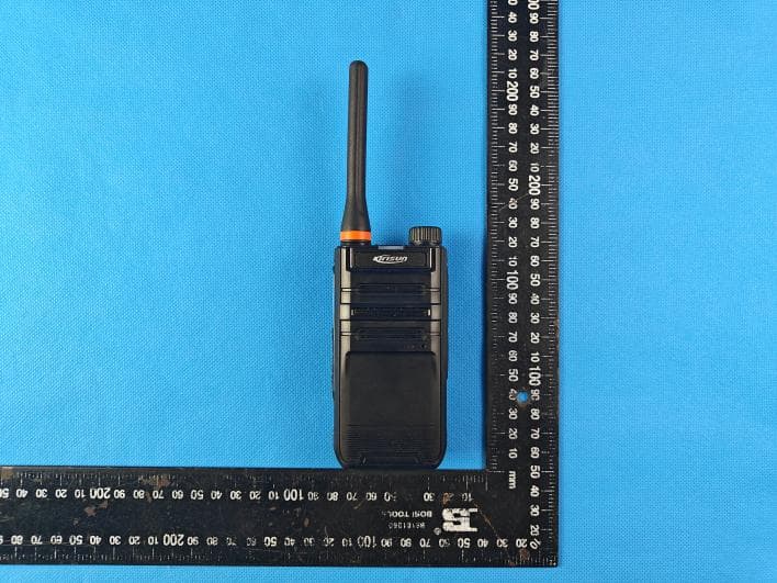
Q5EDP27502
Sep 16, 2024DMR Two Way Radio
Equipment Class
TNF - Licensed Non-Broadcast Transmitter Held to Face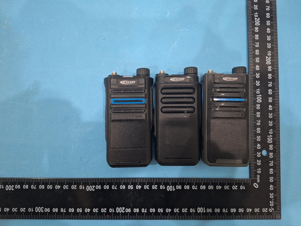
Q5EPT37002
Aug 25, 2024Two Way Radio
Equipment Class
TNF - Licensed Non-Broadcast Transmitter Held to Face