Q78-ZTEMY39CDMA 1X-EVDO Wireless Card
ZTE Corporation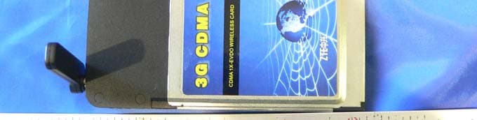
Click to zoom
Application Details
- Equipment Class
- PCB - PCS Licensed Transmitter
- Date of Grant
- Feb 27, 2006
- Application Purpose
- Original Equipment
- Date of Application
- Feb 27, 2006
- Equipment Note
- CDMA 1X-EVDO Wireless Card
- Frequency Range
- 824.70000000 - 848.30000000
- Company
- ZTE Corporation
- Country
- China
Documents & Files
Document Text
Text extracted from the exhibit documents filed with the FCC. Open a document above to read the original.
Users Manual
ZTE CORPORATION ZTE MY39 CDMA 1X-EVDO Wireless Data Card User Manual Retransmission and reproduction in any manner whatsoever without the permission of ZTE is strictly forbidden. All rights reserved. Copyright © 2005 by ZTE Corporation All rights reserved. No part of this publication may be excerpted, reproduced, translated or utilized in any form or by any means, electronic or mechanical, including photocopying and microfilm, without the prior written authorization of ZTE Corporation. ZTE Corporation reserves the right to make modifications on print errors or update specifications in this manual without notice. Edition 1 st edition, July, 2005 10 9 8 7 6 5 4 3 2 1 Retransmission and reproduction in any manner whatsoever without the permission of ZTE is strictly forbidden. All rights reserved. Contents 1 Welcome.............................................................................................................................1 1.1 Introduction............................................................................................................1 1.2 Warning and Notice..............................................................................................1 1.3 Software Drivers License...................................................................................2 1.4 System requirements...........................................................................................3 1.5 Specification..........................................................................................................3 2 Installation.........................................................................................................................4 2.1 Package Checking................................................................................................4 2.2 Outline and Part Introduction...........................................................................4 2.3 Software Installation...........................................................................................4 2.4 Hardware Installation..........................................................................................8 2.5 Safe removal of Hardware.................................................................................9 2.6 Getting started....................................................................................................10 2.7 Software Uninstallation.....................................................................................11 3 Functions & Operation..................................................................................................11 3.1 Interface introduction........................................................................................11 3.1.1 Main Interface............................................................................................11 3.1.2 Description of Mini Icons........................................................................11 3.2 Connecting to Internet......................................................................................12 3.3 History....................................................................................................................13 3.4 Messages...............................................................................................................13 3.4.1 Creating new message...........................................................................14 3.4.2 Viewing Received Messages and Sent Messages.........................14 3.4.3 Setting.........................................................................................................15 3.5 Contact...................................................................................................................15 3.6 Setting....................................................................................................................16 3.6.1 Security Settings......................................................................................17 3.6.2 Networks.....................................................................................................17 3.6.3 Ring tone.....................................................................................................18 3.6.4 Default set..................................................................................................18 3.7 Help.........................................................................................................................18 4 FAQ & Answers..............................................................................................................19 Retransmission and reproduction in any manner whatsoever without the permission of ZTE is strictly forbidden. All rights reserved. 1 Welcome 1.1 Introduction Congratulations on purchasing ZTE MY39 Wireless PC Card! ZTE MY39 is a type of hybrid mode wireless netcard, which is suitable for using under CDMA1X-EVDO network. It fits into the PCMCIA card slot of most windows based laptop computers. It allows you to send and receive SMS (Short Messages Service), connects to internet and has an address book. The manual will provide information needed to get started and effectively use your new ZTE MY39. 1.2 Warning and Notice Before using the ZTE MY39, you must review the Safety Information outlined in this document. General instructions z Do not operate the wireless card in an area where prohibited by the law. Follow any special rules and regulations and obey all signs and notices. Always turn off the host device and remove the wireless card from the card slot when instructed to do so, or when you suspect that it may cause interference or danger. z Please use original accessories or accessories that are authorized by ZTE. Using any unauthorized accessories may affect your wireless card’s performance, and violate related national regulations about telecom terminals. z Do not operate your wireless card in any area where a potentially explosive atmosphere may exist. Spar…
Text truncated - open the document above for the full version.
Cover Letter(s)
Federal Communications Commission Authorization and Evaluation Division Confidentiality Request regarding application for certification of FCC ID: Q78-ZTEMY39. Pursuant to Sections 0.457 and 0.459 of the Commission’s Rules, we hereby request confidential treatment of information accompanying this application as outlined below: 1. Block Diagram 2. BOM 3. Operational description 4. Schematic Circuit Diagram The above materials contain trade secrets and proprietary information not customarily released to the public. The public disclosure of these materials may be harmful to the applicant and provide unjustified benefits to its competitors. The applicant understands that pursuant to Section 0.457 of the Rules, disclosure of this application and all accompanying documentation will not be made before the date of the Grant for this application. Sincerely Yours, Signature: Typed or Printed Name: Royce Wang Title: Director Company Name: ZTE Corporation
External Photos
ZTE Corporation FCC ID: Q78-ZTEMY39 EXHIBIT C - EUT PHOTOGRAPHS EUT - Top View EUT - Bottom View ZTE Corporation FCC ID: Q78-ZTEMY39 EUT - Port View
ID Label/Location Info
EXHIBIT A - FCC ID LABELING AND WARNING STATEMENT Proposed FCC ID Label Specifications : Text is black or white in color and is left justified. Labels are silk-screened and shall be “permanently affixed” at a conspicuous location on the EUT. Proposed Label Location on EUT Bottom View of the EUT/Proposed ID Label Location FCC Warning Statement A FCC Warning Statement is provided in the product manual. FCC ID: Q78-ZTEMY39 Industry Canada Industrie Canada IC: 5200A-ZTEMY39 Model Name: ZTE MY39 Made by: ZTE Corporation
Internal Photos
ZTE Corporation FCC ID: Q78-ZTEMY39 EUT - Component View EUT - Solder View ZTE Corporation FCC ID: Q78-ZTEMY39 EUT - Close View 1 EUT - Close View 2
Parts List/Tune Up Info
Tuning Up Procedure & Operational Manual 1 of 41 ZTE Proprietary & Confidential Tuning Up Procedure & Operational Manual Model: Model: Model: Model: ZTE ZTEZTE ZTE MY39 MY39MY39 MY39 Version 1.0 Version 1.0Version 1.0 Version 1.0 8 88 8, , , , Feb FebFeb Feb. .. . 2006 20062006 2006 ZTE CORPORATION 1.0 Objective This document is intended for FCC testing; it mainly includes Tuning Up Procedure and Operational Manual. It describes the key principles of ZTE MY39; its tuning up, its operation among the interfaces and its antenna features. 2.0 Abbreviation and glossary CDMA Code Division Multiple Access EVDO Evolution Data Optimized Tuning Up Procedure & Operational Manual 2 of 41 ZTE Proprietary & Confidential GPS Global positioning system ARM Advanced RISC Machines ADC Analog-to-digital converter AEC Acoustic Echo Cancellation AGC Automatic Gain Control ASIC Application Specific Integrated Circuit CODEC Coder-Decoder DSP Digital Signal Processor EBI External Bus Interface GPIO General-purpose Input/Output USB Universal Serial Bus UART Universal Asynchronous Receiver/Transmitter JTAG Joint Test Action Group (ANSI/ICEEE Std. 1149.1–1990) PA Power Amplifier RF Radio Frequency Tx Transimit Rx Receive TCXO Temperature Compensated Crystal Oscillator LPSDRAM Low Power Synchronous Dynamic Random Access Memory ZIF Zero Intermediate Frequency Tuning Up Procedure & Operational Manual 3 of 41 ZTE Proprietary & Confidential 3.1 Principle of Rx Circuit 3.1.1 ZTE MY39 supports quad bands: CDMA 1X CELLULAR 800/PCS 1900, CDMA EVDO CELLULAR 850/PCS 1900. CELLULAR: PCS: Channel Range :1-799/991-1023 Channel Range :0-1199 Downlink:869MHZ-894MHZ Downlink:1930MHZ-1990MHZ Uplink: 824MHZ-849MHZ Uplink:1850MHZ-1910MHZ Duplexer:45 MHZ Duplexer:60 MHZ Bandwidth:1.25MHZ Bandwidth:1.25MHZ Power Range:<=23~30dBm Power Range:<=23~30dBm 3.1.2 MY39 Block Diagram for Primary Receive Path: :: : The Block Diagram of RX 3.1.3 Signal is coming from the RF Connector. RF Connector is designed for testing; with the RF cable and equipment our test engineers can analyze the Rx/Tx signal through the RF Connector. The Signal goes into Diplexer from the RF Connector to control the working status. After the signal comes out from Diplexer, it goes into the related Duplexer. Then the signals coming from two Duplexer go into LNA(RFL6000). Tuning Up Procedure & Operational Manual 4 of 41 ZTE Proprietary & Confidential After coming out from LNA, they go into the related RF SAW, and they turn into two signals, espectively. RL101 and RR101 are very important two chip sets. For the receive part, they mainly completes: LNAs(Low Noise Amplifiers), Down-Converting Mixers, Low Pass Filters and so on. For example: signal from PCS path comes out PLNA. After LNA and PCS SAW,A Quadrature Downconvertor mixes down the received signal to baseband. The output baseband signals (IP, IM, QP, QM) after filter and amplifier come out of Pin30、Pin31、Pin33、Pin34 and input to the W21, V21, Y26, Y25 of MSM6500. The Mixers gains and the LNA gains are set via a standard 3-wire serial bus. Tuning Up Procedure & Operational Manual 5 of 41 ZTE Proprietary & Confidential The baseband signals inside the Baseband Processor(MSM6500) will be proceeded with analog to digital conversion、decoding、digital processor、digital to analog conversion, DSP and so on. 3.1.4 The primary receive path circuit tuning up Receiver key parameters include: RX Sensitivity、RX Dynamic range、Single tone desensitization, Intermodulation Spurious Response Attenuation, etc. Here are the equipment we need to analyzer the problems(Such as. CDMA 1X and EVDO): a. Set Agilent8960 to the specific channel and set the basestation output -55dBm. b. Power on the netcard,the mobile is connected with Agilent8960 by the RF cable, and let the netcard be in the receive & testing mode. c. Power meter and oscilloscope. Step 1:According to the signal block diagram test step by step,first get rid of FL0(Diplexer), in this way we can avoid the interference from the backwards and test the input signal to the FL0. If the signal is kind of small, we should check the input to FL0, it might be the problem with L102, R110, C105; otherwise it might be the problem with S101. Tuning Up Procedure & Operational Manual 6 of 41 ZTE Proprietary & Confidential Step 2:Solder the FL0 on,test if its output signal attenuation is big,if it is big, it might have something to do with L102, R110, C105, S101. Step 3:Test if LNA output signals are normal or not, by testing pin13 or pin11, usually it might be the problem with L104, L105 or L106, L107 if RL101 solder well. Step 4: Test if RR101 input signals are normal or not, by testing pin40, pin2 or pin6, pin8, usually it might be the problem with FL3, FL4, they solder badly. Step 5:solder all devices on, If and we cannot find the problem,it should be the problem with PCB. 3.1.5 MY39 Block Diagram for Secondary Receive Path: :: : The block diagram of secondary receive path is similar to the block diagram of primary receive path, except the two duplexers are substituted by the two filters. In addition to, The output baseband signals (IP, IM, QP, QM) after filter and amplifier come out of Pin30、Pin31、Pin33、Pin34 and input to the W26, V25, U23, U21 of MSM6500. 3.2 Principle of TX Circuit 3.2.1 Transmit path circuit block diagram Tuning Up Procedure & Operational Manual 7 of 41 ZTE Proprietary & Confidential The Block Diagram of TX 3.2.2 Digital signal by DSP, encoding, D\A conversion into RFT6100(U401), output from B14, A14, B13, A13 of MSM6500 and input into Pin35, Pin36, Pin33, Pin34 of U401. The transmit section of U401 consists of a quadrature upconvertor, amplifier, a Tx VCO, RX PLL, TX PLL, Gain control circuits and so on. RX VCO is outside it. These components implement a translation loop modulator for directly modulating baseband signals. An integrated power control loop is used to control the power amplifier’s output level. RF signal comes out of RF-PA(NA401or NA402) and transmits from the …
Text truncated - open the document above for the full version.
Parts List/Tune Up Info
秘密▲ 本文中的所有信息均为中兴通讯股份有限公司内部资料,不得向外传播 第 1 页 共 6页 Tune-Up Procedure I. Switch the Agilent E5515C Power On 1. Switch on the E5515C using the mains switch at the left bottom corner. 2. Press SHIFT button followed by pressing Preset button on the front panel to initial E5515C. II. Connect the E5515C to the computer Connect the E5515C and the computer with GPIB cable. The computer must have GPIB interface card and GPIB driver having installed. III. Connect the EVDO Card to the Computer Laptop computer : Insert EVDO Card to laptop’s PCMCIA TypeII slot and install corresponding USB driver to make the EVDO Card working with laptop. Personal Computer: Install a PCI->PCMCIA(Type II) transform card in the PC’s main board. Insert EVDO Card to transform card’s slot and install corresponding USB driver to make the EVDO Card working with PC. IV. Connect the EVDO Card to the E5515C 1. Connect the bi-directional RF connector RF IN/OUT of the E5515C to the main antenna RF test connector of the EVDO Card. 2. Open the ZTE Calibration software by double clicking the software icon. The following window will be displayed: 秘密▲ 本文中的所有信息均为中兴通讯股份有限公司内部资料,不得向外传播 第 2 页 共 6页 3. Under the configuration menu there are five sub menu items: Calibration Configuration, Port Configuration, Database Configuration, Time Configuration, Threshold Configuration. The following graph shows the configuration menu. 4.Select Calibration configuration menu to set RF cable loss of Band Class 0(US Cell) and Band Class 1(US PCS). 5.Select Port configuration menu to set correct communication port of the EVDO Card. 秘密▲ 本文中的所有信息均为中兴通讯股份有限公司内部资料,不得向外传播 第 3 页 共 6页 6.Select Database configuration menu to set ODBC database source used by calibration program. The ODBC database source is set through ODBC database manager in Control Panel of windows system. 秘密▲ 本文中的所有信息均为中兴通讯股份有限公司内部资料,不得向外传播 第 4 页 共 6页 V. Go to “Start” 1. Click the “Start” button, you will see the following screen. Once the start button is clicked, the E5515C will check various parameters automatically(e.g. RSSI, Output Power, etc.) and the calibration program will calculate and set different parameters for the EVDO Card accordingly(e.g. Gain, Output Power, etc.) 2. Due to the diversity antenna used by EVDO Card, the calibration program will show a message box “start diversity calibration, please change RF connection to diversity antenna RF test connector” after finishing main receiver’s calibration. The main RF test connector and diversity RF test connector’s position is showed in the following picture: Main Antenna RF Test Connector Diversity Antenna RF Test Connector 秘密▲ 本文中的所有信息均为中兴通讯股份有限公司内部资料,不得向外传播 第 5 页 共 6页 3. If “Calibration Success!” data appears, the EVDO Card has been successfully calibrated and everything is properly tuned. This calibration process typically takes less than 5 minutes if all the above steps are followed and the conditions are met. 秘密▲ 本文中的所有信息均为中兴通讯股份有限公司内部资料,不得向外传播 第 6 页 共 6页
RF Exposure Info
Note: This test report is specially limited to the above client company and this particular sample only. It may not be duplicated without prior written consent of Bay Area Compliance Laboratory Corporation. This report must not be used by the client to claim product certification, approval, or endorsement by NVLAP, NIST or any agency of the U.S. Government. SAR EVALUATION REPORT For ZTE Corporation ZTE Plaza, Hi-tech Park, Nanshan District, Shenzhen, Guangdong, China 518057 FCC ID: Q78-ZTEMY39 This Report Concerns: Original Report Equipment Type: CDMA1X-EVDO PMCIA Card Test Engineer: Snell Leong / Report No.: R0601253S Report Date: 2006-02-10 Reviewed By: Daniel Deng / Prepared By: Bay Area Compliance Laboratory Corporation 1274 Anvilwood Ave. Sunnyvale, CA 94089 Tel: (408) 732-9162 Fax: (408) 732 9164 ZTE Corporation. FCC ID: Q78-ZTEMY39 Report #R0601253S.doc SAR Evaluation Report Page 2 of 77 DECLARATION OF COMPLIANCE SAR EVALUATION Rule Part(s): CFR47 §2.1093 Test Procedure(s): FCC OET Bulletin 65 Supplement C Device Classification: Licensed Mobile Transmitter Device Type: CDMA1X-EVDO Wireless Card FCC ID: Q78- ZTEMY39 Modulation: CDMA 1X-EVDO TX Frequency Range: 800/ 1900MHz Max. Conducted Power Tested: 22.58dBm (836.52MHz)/ 25.95dBm (1880MHz) Antenna Type(s): External Antenna Body-Worn Accessories: None Face-Head Accessories: None Max. SAR Level(s) Measured: 0.503 mW/g (850MHz) & 0.552 mW/g (1900MHz) BACL Corp. declares under its sole responsibility that this wireless portable device has been determined to be in compliance for localized specific absorption rate (SAR) for uncontrolled exposure and general population exposure limits specified in EN 50361:2001 and has been tested in accordance with the measurement procedures specified in ANSI IEEE C95.3:2002 All measurements reported herein were performed under my supervision and believed to be accurate to the best of my knowledge. I further attest for the completeness of these measurements and vouch for the qualifications any and all personnel performing such measurements. The results and statements contained in this report pertain only to the device(s) evaluated. /signature/ Snell Leong Bay Area Compliance Laboratory Corp. ZTE Corporation. FCC ID: Q78-ZTEMY39 Report #R0601253S.doc SAR Evaluation Report Page 3 of 77 TABLE OF CONTENTS REFERENCE, STANDARDS, AND GUILDELINES ...............................................................................................4 SAR LIMITS.................................................................................................................................................................5 EUT DESCRIPTION ....................................................................................................................................................6 DESCRIPTION OF TEST SYSTEM ..........................................................................................................................7 MEASUREMENT SYSTEM DIAGRAM.............................................................................................................................9 SYSTEM COMPONENTS...............................................................................................................................................11 TESTING EQUIPMENT............................................................................................................................................20 EQUIPMENTS LIST & CALIBRATION INFO...................................................................................................................20 SAR MEASUREMENT SYSTEM VERIFICATION ..............................................................................................21 SYSTEM ACCURACY VERIFICATION...........................................................................................................................21 EUT TEST STRATEGY AND METHODOLOGY .................................................................................................23 SAR EVALUATION PROCEDURE.................................................................................................................................23 CONCLUSION ............................................................................................................................................................24 SAR TEST DATA........................................................................................................................................................24 APPENDIX A – MEASUREMENT UNCERTAINTY ............................................................................................25 APPENDIX B – PROBE CALIBRATION CERTIFICATES .................................................................................27 APPENDIX C – DIPOLE CALIBRATION CERTIFICATES ...............................................................................38 APPENDIX D - TEST SYSTEM VERIFICATIONS SCANS .................................................................................54 LIQUID MEASUREMENT RESULT................................................................................................................................54 APPENDIX E - EUT SCANS .....................................................................................................................................57 APPENDIX F – CONDUCTED OUTPUT POWER MEASUREMENT ...............................................................69 PROVISION APPLICABLE.............................................................................................................................................69 TEST PROCEDURE......................................................................................................................................................69 TEST EQUIPMENT.......................................................................................................................................................69 TEST RESULTS................................................…
Text truncated - open the document above for the full version.
RF Exposure Info
ZTE Corporation. FCC ID: Q78-ZTEMY39 Report #R0601253S.doc SAR Evaluation Report Page 38 of 77 APPENDIX C – DIPOLE CALIBRATION CERTIFICATES ZTE Corporation. FCC ID: Q78-ZTEMY39 Report #R0601253S.doc SAR Evaluation Report Page 39 of 77 ZTE Corporation. FCC ID: Q78-ZTEMY39 Report #R0601253S.doc SAR Evaluation Report Page 40 of 77 ZTE Corporation. FCC ID: Q78-ZTEMY39 Report #R0601253S.doc SAR Evaluation Report Page 41 of 77 ZTE Corporation. FCC ID: Q78-ZTEMY39 Report #R0601253S.doc SAR Evaluation Report Page 42 of 77 ZTE Corporation. FCC ID: Q78-ZTEMY39 Report #R0601253S.doc SAR Evaluation Report Page 43 of 77 ZTE Corporation. FCC ID: Q78-ZTEMY39 Report #R0601253S.doc SAR Evaluation Report Page 44 of 77 ZTE Corporation. FCC ID: Q78-ZTEMY39 Report #R0601253S.doc SAR Evaluation Report Page 45 of 77 ZTE Corporation. FCC ID: Q78-ZTEMY39 Report #R0601253S.doc SAR Evaluation Report Page 46 of 77 ZTE Corporation. FCC ID: Q78-ZTEMY39 Report #R0601253S.doc SAR Evaluation Report Page 47 of 77 ZTE Corporation. FCC ID: Q78-ZTEMY39 Report #R0601253S.doc SAR Evaluation Report Page 48 of 77 ZTE Corporation. FCC ID: Q78-ZTEMY39 Report #R0601253S.doc SAR Evaluation Report Page 49 of 77 ZTE Corporation. FCC ID: Q78-ZTEMY39 Report #R0601253S.doc SAR Evaluation Report Page 50 of 77 ZTE Corporation. FCC ID: Q78-ZTEMY39 Report #R0601253S.doc SAR Evaluation Report Page 51 of 77 ZTE Corporation. FCC ID: Q78-ZTEMY39 Report #R0601253S.doc SAR Evaluation Report Page 52 of 77 ZTE Corporation. FCC ID: Q78-ZTEMY39 Report #R0601253S.doc SAR Evaluation Report Page 53 of 77 ZTE Corporation. FCC ID: Q78-ZTEMY39 Report #R0601253S.doc SAR Evaluation Report Page 54 of 77 APPENDIX D - TEST SYSTEM VERIFICATIONS SCANS Liquid Measurement Result 2006-02-08 Simulant Freq [MHz] Parameters Liquid Temp [ºC] Target Value Measured Value Deviation Limits [%] ε r 22.0 55.2 55.9 1.27 ±5 σ 22.0 0.97 0.96 -1.03 ±5 Body 835 1g SAR 22.0 8.872 8.51 -4.08 ±10 ε r = relative permittivity, σ = conductivity and ρ=1000kg/m 3 2006-02-08 Simulant Freq [MHz] Parameters Liquid Temp [ºC] Target Value Measured Value Deviation Limits [%] ε r 22.0 53.3 52.0 -2.43 ±5 σ 22.0 1.52 1.57 3.29 ±5 Body 1900 1g SAR 22.0 24.97 25.0 0.12 ±10 ε r = relative permittivity, σ = conductivity and ρ=1000kg/m 3 ZTE Corporation. FCC ID: Q78-ZTEMY39 Report #R0601253S.doc SAR Evaluation Report Page 55 of 77 Date/Time: 2/8/2006 9:02:48 AM Test Laboratory: Bay Area Compliance Lab Corp. File Name: ET_1604_SystemValidationCheck_D835_Body.da4 DUT: Dipole 835 MHz; Type: CD835V3; Serial: CD835V3 - SN:1012 Program Name: System Performance Check at 835 MHz Communication System: CW; Frequency: 835 MHz;Duty Cycle: 1:1 Medium parameters used: f = 835 MHz; σ = 0.96 mho/m; ε r = 55.9; ρ = 1000 kg/m 3 Phantom section: Flat Section DASY4 Configuration: - Probe: ET3DV6 - SN1604; ConvF(6.27, 6.27, 6.27); Calibrated: 3/18/2005 - Sensor-Surface: 4mm (Mechanical Surface Detection) - Electronics: DAE3 Sn456; Calibrated: 10/18/2005 - Phantom: SAM with CRP; Type: Twin SAM; Serial: TP-1032 - Measurement SW: DASY4, V4.5 Build 19; Postprocessing SW: SEMCAD, V1.8 Build 146 d=15mm, Pin=1W/Area Scan (61x121x1): Measurement grid: dx=15mm, dy=15mm Maximum value of SAR (interpolated) = 8.16 mW/g d=15mm, Pin=1W/Zoom Scan : Measurement grid: dx=5mm, dy=5mm, dz=5mm Reference Value = 97.5 V/m; Power Drift = -0.012 dB Peak SAR (extrapolated) = 11.6 W/kg SAR(1 g) = 8.51 mW/g; SAR(10 g) = 4.91 mW/g Maximum value of SAR (measured) = 8.34 mW/g ZTE Corporation. FCC ID: Q78-ZTEMY39 Report #R0601253S.doc SAR Evaluation Report Page 56 of 77 Date/Time: 2/09/2006 9:58:28 AM Test Laboratory: Bay Area Compliance Lab Corp. File Name: DUT: Dipole 1800 MHz; Type: D1800V2; Serial: D1800V2 - SN:5122 Program Name: System Performance Check at 1900 MHz Communication System: CW; Frequency: 1900 MHz;Duty Cycle: 1:1 Medium parameters used: f = 1900 MHz; σ = 1.57 mho/m; ε r = 52; ρ = 1000 kg/m 3 Phantom section: Flat Section DASY4 Configuration: - Probe: ET3DV6 - SN1604; ConvF(4.79, 4.79, 4.79); Calibrated: 3/18/2005 - Sensor-Surface: 4mm (Mechanical Surface Detection) - Electronics: DAE3 Sn456; Calibrated: 10/18/2005 - Phantom: SAM with CRP; Type: Twin SAM; Serial: TP-1032 - Measurement SW: DASY4, V4.5 Build 19; Postprocessing SW: SEMCAD, V1.8 Build 146 d=10mm, Pin=1W/Area Scan (51x91x1): Measurement grid: dx=15mm, dy=15mm Maximum value of SAR (interpolated) = 33.3 mW/g d=15mm, Pin=1W /Zoom Scan: Measurement grid: dx=5mm, dy=5mm, dz=5mm Reference Value = 144.0 V/m; Power Drift = 0.00 dB Peak SAR (extrapolated) = 40.4 W/kg SAR(1 g) = 25.0 mW/g; SAR(10 g) = 14 mW/g Maximum value of SAR (measured) = 28.5 mW/g ZTE Corporation. FCC ID: Q78-ZTEMY39 Report #R0601253S.doc SAR Evaluation Report Page 57 of 77 APPENDIX E - EUT SCANS Date/Time: 2/8/2006 4:53:08 PM Test Laboratory: Bay Area Compliance Lab Corp. COMPAQ LAPTOP -H DUT: ZTE CDMA 1X EDVO WIRELESS CARD; Type: Sample; Serial: 699ECA25 Communication System: CDMA; Frequency: 836.52 MHz;Duty Cycle: 1:1 Medium parameters used (interpolated): f = 836.52 MHz; σ = 0.96 mho/m; ε r = 55.9; ρ = 1000 kg/m 3 Phantom section: Flat Section DASY4 Configuration: • Probe: ET3DV6 - SN1604; ConvF(6.27, 6.27, 6.27); Calibrated: 3/18/2005 • Sensor-Surface: 4mm (Mechanical Surface Detection) • Electronics: DAE3 Sn456; Calibrated: 10/18/2005 • Phantom: SAM with CRP; Type: Twin SAM; Serial: TP-1032 • Measurement SW: DASY4, V4.6 Build 23; Postprocessing SW: SEMCAD, V1.8 Build 160 COMPAQ LAPTOP/Area Scan (71x81x1): Measurement grid: dx=15mm, dy=15mm Info: Interpolated medium parameters used for SAR evaluation. Maximum value of SAR (interpolated) = 0.457 mW/g COMPAQ LAPTOP/Zoom Scan (5x5x5): Measurement grid: dx=5mm, dy=5mm, dz=5mm Reference Value = 21.4 V/m; Power Drift = -0.098 dB Peak SAR (extrapolated) = 0.471 W/kg SAR(1 g) = 0.460 mW/g; SAR(10 g) = 0.440 mW/g Info: Interpolated medium parameters used for SAR evaluation. Maximum value of SAR (measured) = 0.470 mW/g 0 dB = 0.470mW/g Plot #1 ZTE Corporation. FCC ID:…
Text truncated - open the document above for the full version.
Test Report
Note: This test report is specially limited to the above client company and this particular sample only. It may not be duplicated without prior written consent of Bay Area Compliance Laboratory Corporation. This report must not be used by the client to claim product certification, approval, or endorsement by NVLAP, NIST or any agency of the U.S. Government. FCC PART 22, 24 TYPE APPROVALS EMI MEASUREMENT AND TEST REPORT For ZTE Corporation ZTE Plaza, Hi-tech Park, Nanshan District, Shenzhen, Guangdong, China 518057 FCC ID: Q78-ZTEMY39 This Report Concerns: Original Report Equipment Type: 800/1900 MHz CDMA 1X-EVDO PCMCIA Card Test Engineer: Snell Leong / Report No.: R0601253 Report Date: 2006-02-09 Reviewed By: Daniel Deng / Prepared By: Bay Area Compliance Laboratory Corporation (BACL) 1274 Anvilwood Ave. Sunnyvale, CA 94089 Tel: (408) 732-9162 Fax: (408) 732 9164 ZTE Corporation FCC ID: Q78-ZTEMY39 Report # R0601253Rpt-a.doc Page 2 of 34 FCC Part 22, 24 Type Approvals Report TABLE OF CONTENTS GENERAL INFORMATION.......................................................................................................................................4 PRODUCT DESCRIPTION FOR EQUIPMENT UNDER TEST (EUT) ...............................................…
Text truncated - open the document above for the full version.
Contact Information
Applicant
Cary Kong(Product Certification Manager)
Test Firm
Bay Area Compliance LaboratoryJohn Chan
Technical Specifications
| # | Rule Parts | Frequency Range | Power Output | Emission | Tolerance |
|---|---|---|---|---|---|
| 2 | 22H | 824.7 MHz - 848.3 MHz | 181.00 mW | 1M25F9W | 2.5 ppm |
Other Applications from ZTE Corporation

Q78-E1320
Oct 06, 2022Home Gateway
Equipment Class
NII - Unlicensed National Information Infrastructure TX
Q78-E3330
Sep 21, 2022Home Gateway
Equipment Class
JBP - Part 15 Class B Computing Device Peripheral
Q78-ZXV10B866V2
May 23, 2021RichMedia Box
Equipment Class
DTS - Digital Transmission System
Q78-ZXHNH298Q
Apr 22, 2021Home Gateway
Equipment Class
NII - Unlicensed National Information Infrastructure TX
Q78-ZXHNH196Q
Apr 19, 2021Home Gateway
Equipment Class
NII - Unlicensed National Information Infrastructure TX