QVY56PMio LINK - Strapless Continuous Heart Rate Monitor
Physical Enterprises Inc.
Click to zoom
Application Details
- Equipment Class
- DXX - Part 15 Low Power Communication Device Transmitter
- Date of Grant
- Mar 24, 2014
- Application Purpose
- Original Equipment
- Date of Application
- Mar 24, 2014
- Equipment Note
- Mio LINK - Strapless Continuous Heart Rate Monitor
- Frequency Range
- 2457.00000000 - 2457.00000000
- Company
- Physical Enterprises Inc.
- Country
- Canada
Documents & Files
Document Text
Text extracted from the exhibit documents filed with the FCC. Open a document above to read the original.
Users Manual
Complete User Guide Table of Contents Welcome 03 Getting Started 04 Your Mio LINK 04 Activating Mio LINK 04 Wearing Your Mio LINK Using Mio LINK 05 Getting Your Heart Rate 06 Heart Rate Zones 07 Customizing Heart Rate Zones 08 Using Mio LINK With Devices And Apps Maintaining Your Mio LINK 10 Charging The Battery 11 Using Mio LINK In Water 11 Caring For Your Mio LINK 12 Mio LINK Specifications Warranty And Regulations 12 Warranty & Service 14 Exclusions And Limitations Of Liability; Disclaimers 14 Copyright And Trademarks 15 Regulations And Conformity Have any questions about your Mio LINK? We’re ready to help! Your complete satisfaction is our goal, so your feedback is crucial. If you have any thoughts, questions, or concerns, just contact our knowledgeable support team at: 1.877.770.1116 [email protected] facebook.com/mioglobal twitter.com/mioglobal Welcome Congratulations on your purchase of Mio LINK, the performance level, strapless, continuous heart rate monitor that you can wear on your wrist. LINK uses ANT+™ and Bluetooth® Smart technology to transmit your heart rate data to smartphones and other compatible devices. Download the Mio GO app for a fully personalized, interactive workout, or take advantage of hundreds of other fitness apps. Remember to register your Mio LINK online at mioglobal.com/register for full warranty service. Getting Started What’s Included 1. Mio LINK 2. USB Dongle 3. Quick Start Guide Important Safety Information Consult your doctor before beginning a new exercise program. Mio LINK provides very accurate heart rate measurements. However, it is not a medical device. The LINK and USB dongle contain strong magnets. If you use a pacemaker, defibrillator, or other implanted electronic devices, consult your doctor before using a Mio LINK. See Charging The Battery for important battery care and battery safety information. Your Mio LINK Activating Mio LINK 1. Remove Mio LINK from the packaging. 2. Fasten the LINK onto your wrist. 3. Press and hold the button to activate your LINK. The LED will light up. 4. After a few seconds, the LED light will turn off. 5. Your LINK is now activated and in standby mode. Wearing Your Mio LINK To accurately monitor your heart rate: Fasten Mio LINK snugly on your wrist. The optical sensor on the back should make good contact with your skin. You should wear the LINK above, and not directly on top, of your wrist bone If you have a smaller wrist, wear the LINK higher on your forearm. If you use the LINK for biking, wear the LINK higher on your forearm, since the bending of the wrist will affect the heart rate reading. If you often have cold hands or poor circulation, try exercising for a few minutes to increase blood flow before you begin to track your heart rate. Using Mio LINK Getting Your Heart Rate You can get your real-time heart rate when you put Mio LINK in Heart Rate (HR) Mode. You must be wearing the LINK to obtain an accurate heart rate reading. The heart rate may take a few seconds to Button LED Optical Sensor USB Connector Charging Pins Charging Pins stabilize while your body is adjusting to the physical activity; we recommend activating Heart Rate Mode during the warm up stage of your workout. Turning On HR Mode 1. Press and hold the Button until the LED lights up. The colour of this LED is an indicator of the battery level. (See Charging The Battery for more information). 2. Mio LINK will immediately begin searching for your HR, indicated by the pulsing LED light. 3. Hold your arm still until the LED blinks in a distinctively slower pattern. This means the LINK has found your heart rate. The LED colour at this point is an indicator of the HR zone. For more details, please refer to Heart Rate Zones. If no valid heart rate signal is found within the initial 2 minutes, the LED will light up in red for 2 seconds, then the LINK will automatically leave Heart Rate Mode and turn off. Please refer to Troubleshooting. During your workout, if you see a red LED flashing in a steady pattern (ON for 1 second, OFF for 1 second), the LINK has lost connection to your heart rate. Please refer to Troubleshooting. Turning Off HR Mode Press and hold the Button until the LED lights up for 2 seconds. 1. The colour of this LED indicates the battery level. (See Charging The Battery for more information). Troubleshooting Minimize wrist movement when Mio LINK is searching for your initial heart rate. You may need to tighten the strap. Try wearing the LINK higher on your forearm. On colder days, activate the heart rate reading before heading outdoors. If you are still having trouble, try wearing the LINK on your other wrist. Heart Rate Zones Your target heart rate (HR) zone consists of your upper HR limit and your lower HR limit. These limits are usually a percentage of your maximal heart rate (MHR). If you do not know your MHR or upper and lower HR limits, you can check with your doctor, or use this following MHR calculation method as a guidance: Using Heart Rate Zone Alerts Training Zone Mode (5-Zone) The LED light will blink slowly to indicate your current HR zone. You can customize the upper and lower boundaries of each HR zone through the Mio GO app. Please see Customizing Heart Rate Zones for more details. COLOUR DESCRIPTION LOWER HR LIMIT UPPER HR LIMIT Cyan ● Resting 0% of MHR < 50% of MHR Blue ● Warm Up / Recovery 50% of MHR < 60% of MHR Green ● Fat Burn & Endurance 60% of MHR < 70% of MHR Yellow ● Aerobic Fitness 70% of MHR < 80% of MHR Magenta ● Anaerobic Intensive 80% of MHR < 90% of MHR Red ● Peak Performance 90% of MHR 220 BPM Note: This table is only a suggested ranger. Zone Alert Mode (3-Zone) Training Zone Mode is the factory default on Mio LINK. To switch to Zone Alert Mode, or to customize the upper and lower boundaries of each HR zone, please refer to Customizing Heart Rate Zones. In Zone Alert Mode, the LED will blink slowly to indicate whether you are below, within, or above the target HR zone. A double …
Text truncated - open the document above for the full version.
Block Diagram
MAIN MCU NORDIC nRF51422 RECHARGEABLE BATTERY RECHARGER IC 2.7V REGULATOR 5V REGULATOR UI LED & 1 BUTTON OHR MCU TI MSP430F5510 5V POWER USB SOCKET AMPLIFIER CIRCUITRY OPTICAL SENSOR & LEDs ACCEL. SENSOR OHR MODULE FLASH IN FIRMWARE (FOR FACTORY ASSEMBLY ONLY) POWER MANAGEMENT 16MHz 8MHz 32768 Hz ANT BLOCK DIAGRAMPHYSICAL ENTERPRISES INCBRAND: MIOMODEL NAME: MIO LINKMODEL #: 56P BAL ST NRF01D3 Page 9 nRF51422 Product Specification v2.1 2 Product overview 2.1Block diagram Figure 1 Block diagram nRF51 AHB TO APB BRIDGE RADIO AHB-LITE BUS slave TIMER 2 ARM CORTEX-M0 ECB DAPNTB CODERAM TEMP QDEC LPCOMP WDT NVMC ADC GPIOTE GPIO master slave ANT1 ANT2 P0 (P0.0 – P0.31) POWER SWDIO SWCLK RESET SCK MISO MOSI LED A B slave RTC0 PPI slave UART RXD TXD CTS RTS CLOCK XL2 XL1 XC2 XC1 TWI0 SCL SDA TIMER 0 TIMER 1 RTC1 NVIC SPIS1 SCK MISO MOSI TWI1 SCL SDA FICR slave UICR slave SPI0 SPI1 SCK MISO MOSI RNG AIN0 – AIN7 AIN0 – AIN7 CCM AAR
External Photos
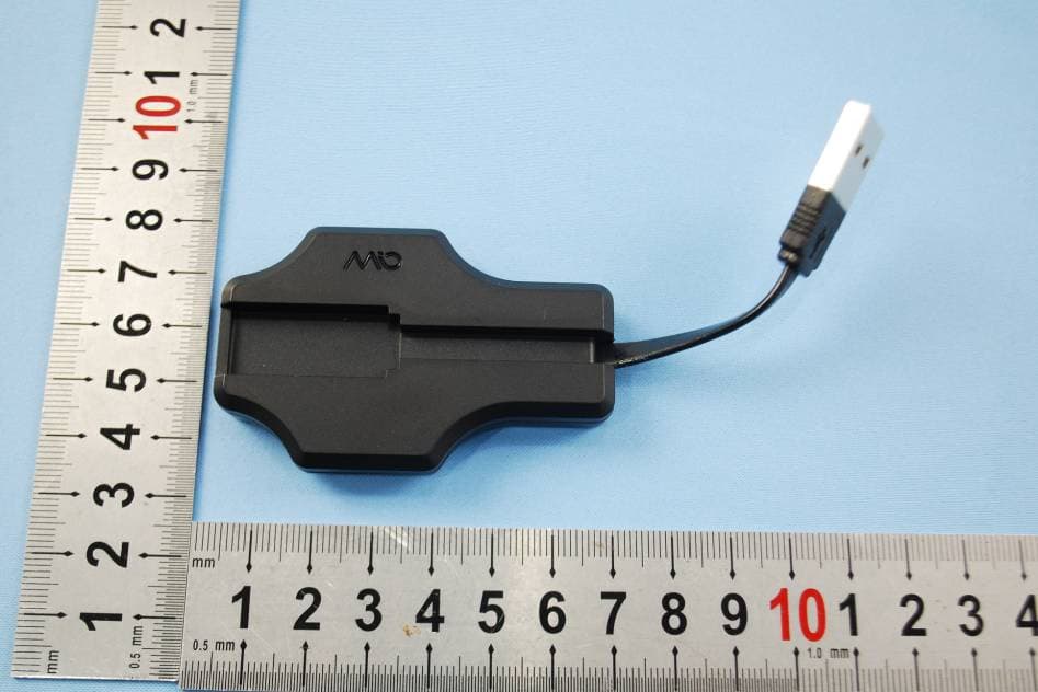
INTERTEK TESTING SERVICE Report No.: 14011109HKG-001 FCC ID: QVY56P IC: 10714A-56P Equipment Photographs Model : 56P (External) INTERTEK TESTING SERVICE Report No.: 14011109HKG-001 FCC ID: QVY56P IC: 10714A-56P Equipment Photographs Model : SW2782(BA) (External)
ID Label/Location Info
6mm 6.4MM6.4MM 6.4MM5.5MM 6.4MM 7.2MM 5mm6mm CU:MIO SIZE:13X1.5MM(+/-1MM) COLOR:WHITE ON TRANSPARENT MATERIAL:0.12MM PET(SELF ADHESIVE LABEL) FINISHING:W/ MATT PP COATING CU:MIO SIZE:6.4X6.4MM(+/-1MM) COLOR:WHITE ON TRANSPARENT MATERIAL:0.12MM PET(SELF ADHESIVE LABEL) FINISHING:W/ MATT PP COATING CU:MIO SIZE:6.4X5.5MM(+/-1MM) COLOR:WHITE ON TRANSPARENT MATERIAL:0.12MM PET(SELF ADHESIVE LABEL) FINISHING:W/ MATT PP COATING LABEL LOCATION 1.5MM1.5MM 13MM13MM MODEL:56P CHINA SN:56P000001JK FCC ID: QV Y56 P IC:10 714A-5 6P IC:10 714A-5 6P FCC ID: QV Y56 P LABEL LOCATION
Internal Photos
INTERTEK TESTING SERVICE Report No.: 14011109HKG-001 FCC ID: QVY56P IC: 10714A-56P Equipment Photographs Model: 56P (Internal) INTERTEK TESTING SERVICE Report No.: 14011109HKG-001 FCC ID: QVY56P IC: 10714A-56P Equipment Photographs Model: 56P (Internal) INTERTEK TESTING SERVICE Report No.: 14011109HKG-001 FCC ID: QVY56P IC: 10714A-56P Equipment Photographs Model: 56P (Internal) INTERTEK TESTING SERVICE Report No.: 14011109HKG-001 FCC ID: QVY56P IC: 10714A-56P Equipment Photographs Model: 56P (Internal) INTERTEK TESTING SERVICE Report No.: 14011109HKG-001 FCC ID: QVY56P IC: 10714A-56P Equipment Photographs Model: 56P (Internal) INTERTEK TESTING SERVICE Report No.: 14011109HKG-001 FCC ID: QVY56P IC: 10714A-56P Equipment Photographs Model: 56P (Internal) INTERTEK TESTING SERVICE Report No.: 14011109HKG-001 FCC ID: QVY56P IC: 10714A-56P Equipment Photographs Model: 56P (Internal)
Operational Description
Technical Description: The Equipment Under Test (EUT) is a portable heart rate sensor, equipped with USB, Bluetooth 4.0 and ANT+ Interface. The EUT operates in frequency 2457MHz at ANT+ (1 channel with 1MHz spacing) and also operates in the frequency range 2402MHz to 2480MHz at Bluetooth 4.0 (40 channels with 2MHz spacing). The EUT is powered by 1 X 3.7V rechargeable battery (Li- Poly). The USB interface of the EUT do not contain PC Connectivity which the USB interface is for charging use only. The brief circuit description is listed as follows: 1. Bluetooth 4.0 and ANT+ RF Portion 1) U3 (nRF51422) is a single-chip ANT+ and Bluetooth 4.0+EDR compliant 2.4GHz RF SoC processor. 2) Y3 is 32.768 kHz crystal for Real Time Clock. 3) Y1 is 16MHz crystal oscillator providing clock for U3. 4) U7 (AT24C02C) is an I2C compatible serial EEPROM. 2. Microcontroller Portion 1) U12 (MSP430F5510) is mixed signal microcontroller. 2) X13 is 8MHz crystal oscillator providing clock for U12. 3) U20 (MMA8452Q) is a three axes linear accelerometer. 3. Optical Sensor Portion 1) U13 (ADS11115) is a 16-bit analog to digital converter. 2) U8 and U9 (TS5A9411) are analog switches. 3) U3 and U4 (MCP6293) are Rail to Rail Op Amps. 4) U15 (MCP4531) is a Mixed Signal- Digital Potentiometer. 4. USB Charging and power supply circuit Portion 1) U10 (MCP73832) is a charge management controller. 2) U1 (TPS61222) is a 5V step-up voltage converter. 3) U6 (UP49A) is a battery protection IC. 4) U2 (HSNT-4) is a 2.7V voltage regulator. When the ANT+ was stand-alone emitting, the ANT+ portion emission is as below: Antenna Type: Internal integral antenna Antenna Gain: -1.1dBi Production tolerance: -12dBm (Minimum) to -4dBm (Maximum) When the Bluetooth 4.0 was stand-alone emitting, the Bluetooth 4.0 portion emission is as below: Antenna Type: Internal integral antenna Antenna Gain: -1.1dBi Production tolerance: -11dBm (Minimum) to -3dBm (Maximum) Copyright © 2013 Nordic Semiconductor ASA. All rights reserved. Reproduction in whole or in part is prohibited without the prior written permission of the copyright holder. nRF51422 Multiprotocol ANT™/Bluetooth® low energy System on Chip Product Specification v2.1 Key Features •2.4 GHz transceiver • -90 dBm sensitivity in ANT mode • -93 dBm sensitivity in Bluetooth® low energy mode • 250 kbps, 1 Mbps, 2 Mbps supported data rates • TX Power -20 to +4 dBm in 4 dB steps • TX Power -30 dBm Whisper mode • 13 mA peak RX, 10.5 mA peak TX (0 dBm) • RSSI (1 dB resolution) • ARM® Cortex™-M0 32 bit processor • 275 μA/MHz running from flash memory • 150 μA/MHz running from RAM • Serial Wire Debug (SWD) • S200 and S300 series SoftDevice ready •Memory • 256 kB or128 kB embedded flash program memory • 16 kB RAM • On-air compatibility with nRF24L series • Flexible Power Management • Supply voltage range 1.8 V to 3.6 V • 2.5 μs wake-up using 16 MHz RCOSC • 0.6 μA at 3 V OFF mode • 1.2 μA at 3 V in OFF mode + 1 region RAM retention • 2.6 μA at 3 V ON mode, all blocks IDLE • 8/9/10 bit ADC - 8 configurable channels • 31 General Purpose I/O Pins • One 32 bit and two 16 bit timers with counter mode •SPI Master/Slave • Low power comparator • Temperature sensor • Two-wire Master (I2C compatible) •UART (CTS/RTS) • CPU independent Programmable Peripheral Interconnect (PPI) • Quadrature Decoder (QDEC) • AES HW encryption • Real Timer Counter (RTC) • Package variants • QFN48 package, 6 x 6 mm • WLCSP package, 3.50 x 3.83 mm Applications • Personal Area Networks • Health/fitness sensor and monitor devices • Medical devices • Key-fobs + wrist watches • Remote control toys • Home/industrial automation • Environmental sensor networks •Active RFID • Logistics/goods tracking • Audience-response systems • Interactive entertainment devices •Remote control • 3D Glasses •Gaming controller Page 2 nRF51422 Product Specification v2.1 Liability disclaimer Nordic Semiconductor ASA reserves the right to make changes without further notice to the product to improve reliability, function or design. Nordic Semiconductor ASA does not assume any liability arising out of the application or use of any product or circuits described herein. Life support applications Nordic Semiconductor’s products are not designed for use in life support appliances, devices, or systems where malfunction of these products can reasonably be expected to result in personal injury. Nordic Semiconductor ASA customers using or selling these products for use in such applications do so at their own risk and agree to fully indemnify Nordic Semiconductor ASA for any damages resulting from such improper use or sale. Contact details For your nearest distributor, please visit www.nordicsemi.com. Information regarding product updates, downloads, and technical support can be accessed through your My Page account on our home page. RoHS and REACH statement Nordic Semiconductor's products meet the requirements of Directive 2002/95/EC of the European Parliament and of the Council on the Restriction of Hazardous Substances (RoHS) and the requirements of the REACH regulation (EC 1907/2006) on Registration, Evaluation, Authorization and Restriction of Chemicals. The SVHC (Substances of Very High Concern) candidate list is continually being updated. Complete hazardous substance reports, material composition reports and latest version of Nordic's REACH statement can be found on our website www.nordicsemi.com. Main office: Phone: +47 72 89 89 00 Fax: +47 72 89 89 89 Otto Nielsens veg 12 7052 Trondheim Norway Mailing address: Nordic Semiconductor P.O. Box 2336 7004 Trondheim Norway Page 3 nRF51422 Product Specification v2.1 Datasheet Status Revision History StatusDescription Objective Product Specification (OPS) This product specification contains target specifications for product development. Preliminary Product Specification (PPS) This product specification contains preliminary data; supplementary data may be published from Nordic Semiconductor ASA later. Product Specification (PS) …
Text truncated - open the document above for the full version.
RF Exposure Info
INTERTEK TESTING SERVICES FCC ID: QVY56P RF exposure - 1 of 1 For Standalone 10g Extremity SAR test exclusion consideration, when the corresponding 10g Extremity SAR Exclusion Threshold requirement in KDB 447498 is satisfied, standalone 10g Extremity SAR evaluation for general population exposure conditions, by measurement or numerical simulation is not required. Description the tested model: 56P EUT Description : 2.4GHz Bluetooth 4.0 and ANT+ Heart Rate Monitor Model : 56P Operating Configuration(s) : Operating mode (s) : ANT+ Transmitting Device Category : Portable Device Tx Frequency : 2457MHz Production tolerance : -12 dBm (Minimum) to -4 dBm (Maximum) Antenna gain : -1.1 dBi = 0.78 (num gain) Maximum source-based time- averaging duty factor : 100.0% = (1/1 x100%) Minimum separation distance : 5 mm Applicable FCC KDB : FCC KDB 447498 D01 FCC KDB 865664 D02 From above data, the source-based time-averaging output power is as follow: The Maximum Conducted Power = -4 dBm = 0.4 mW The Maximum conducted Power source-based time-averaging output power = (0.4 * 1.000) mW = 0.39810717 mW In the frequency range of 100MHz to 6GHz and test separation distance ≤ 50mm, the 10g Extremity SAR Exclusion Threshold will be determined as follow, 10g Extremity SAR exclusion threshold = () )(/5.7GHzFTD× = 23.92 mW where TD = 5 mm and F(GHz) = 2.46 GHz Conclusion Since the calculated conducted source-based time-averaged output power is 0.40 mW, which is less than the 10g extremity SAR Exclusion Threshold at 5mm test separation distance 23.92 mW for general population and uncontrolled exposure, standalone SAR evaluation for general population exposure conditions, by measurement or numerical simulation is not required.
RF Exposure Info
INTERTEK TESTING SERVICES FCC ID: QVY56P RF exposure - 1 of 1 For Standalone 10g Extremity SAR test exclusion consideration, when the corresponding 10g Extremity SAR Exclusion Threshold requirement in KDB 447498 is satisfied, standalone 10g Extremity SAR evaluation for general population exposure conditions, by measurement or numerical simulation is not required. Description the tested model: 56P EUT Description : 2.4GHz Bluetooth 4.0 and ANT+ Heart Rate Monitor Model : 56P Operating Configuration(s) : Operating mode (s) : Bluetooth 4.0 Transmitting Device Category : Portable Device Tx Frequency : 2402 – 2480 MHz Production tolerance : -11 dBm (Minimum) to -3 dBm (Maximum) Antenna gain : -1.1 dBi = 0.78 (num gain) Maximum source-based time- averaging duty factor : 100.0% = (1/1 x100%) Minimum separation distance : 5 mm Applicable FCC KDB : FCC KDB 447498 D01 FCC KDB 865664 D02 From above data, the source-based time-averaging output power is as follow: The Maximum Conducted Power = -3 dBm = 0.5 mW The Maximum conducted Power source-based time-averaging output power = (0.5 * 1.000) mW = 0.50118723 mW In the frequency range of 100MHz to 6GHz and test separation distance ≤ 50mm, the 10g Extremity SAR Exclusion Threshold will be determined as follow, 10g Extremity SAR exclusion threshold = () )(/5.7GHzFTD× = 23.81 mW where TD = 5 mm and F(GHz) = 2.48 GHz Conclusion Since the calculated conducted source-based time-averaged output power is 0.50 mW, which is less than the 10g extremity SAR Exclusion Threshold at 5mm test separation distance 23.81 mW for general population and uncontrolled exposure, standalone SAR evaluation for general population exposure conditions, by measurement or numerical simulation is not required.
RF Exposure Info
INTERTEK TESTING SERVICES FCC ID: QVY56P RF exposure - 1 of 1 Simultaneous Transmission SAR exclusion considerations Since the ANT+ and Bluetooth 4.0 transmitters of this device may operate simultaneously, simultaneous transmission analysis is required. Per KDB 447498, 10-g extremity simultaneous transmission SAR test exclusion can be applied when the sum of 10-g extremity SAR of all simultaneously transmitting antennas in an operating mode and exposure condition combination is within the SAR limit ( ≤ 4.0 W/kg). When the standalone 10-g extremity SAR test exclusion is applied, the standalone 10-g extremity SAR must be estimated according to the following equation, Estimated 10-g Extremity SAR = )max/()75.18/)((TDPxGHzF where F(GHz) is the RF channel transmit frequency in GHz Pmax is the max. power of channel, including tune-up tolerance, mW TD is the min. test separation distance, mm For ANT+ operation, Maximum Time-averaged Conducted Power of this device = 0.40 mW Therefore, the Estimated 10-g extremity SAR will be determined as follow, Estimated 10-g Extremity SAR = )max/()75.18/)((TDPxGHzF = 0.007 W/kg where Pmax = 0.40mW, TD = 5 mm and F(GHz) = 2.457 GHz For Bluetooth 4.0 operation, Maximum Time-averaged Conducted Power of this device = 0.50 mW Therefore, the Estimated SAR will be determined as follow, Estimated 10-g Extremity SAR = )max/()75.18/)((TDPxGHzF = 0.008 W/kg where Pmax = 0.50mW, TD = 5 mm and F(GHz) = 2.480 GHz Simultaneous Transmission Analysis ANT+ Estimated SAR (W/kg) Bluetooth 4.0 Estimated SAR (W/kg) Σ SAR (W/kg) Simultaneous SAR Required 0.007 0.008 0.015 No Conclusion Since the above summed estimated 10g extremity SAR result for all simultaneous transmission conditions were below the 10g extremity SAR limit (4.0 W/kg), 10g extremity SAR evaluation for simultaneous transmission configuration are not required.
Schematics
Voltage DETECT NOTICE OF RESTRICTIONS. In agreeing to receive this information, including all related materials and documents (the “Information”), the recipient acknowledges and agrees that (i) the Information is the exclusive property of Physi-Cal Enterprises Inc. or its licensors (collectively, “Physi-Cal”), (ii) may be used solely for the purpose of analysis and consideration in relation to the conduct of business with Physi-Cal, (iii) may not be disclosed, reversed engineered, disseminated, translated, copied or reproduced in any manner whatsoever except as expressly authorized in writing by Physi-Cal, (iv) any unauthorized use or disclosure of the Article will cause irreparable harm to Physi-Cal for which monetary damages will not be an adequate remedy, and (v) Physi-Cal has relied upon the recipient having made the acknowledgements and agreements set out in clauses (i) to (iv) in agreeing to make the Information 2014/01/20 MODEL NO. 56P(SE629) MADE BY APPROVED BY ISSUE REVISION DATE: 1 2 QINYU YQIN DCAB SCHEMATIC DIAGRAM CHKD DRAWN: QINYU TITLEDOC NO. CAD REF. OF PAGE APPD.: YQIN ABCD 6 5 3 4 2 1 FIRST RELEASE FOR PRODUCTION 1.0 R27 39K 0.5% R28 10k 0.5% C42 100nF C16 1nF 1 VDD 2 DCC 3 P0.30 4 P0.00 5 P0.01 6 P0.02 7 P0.03 8 P0.04 9 P0.05 10 P0.06 11 P0.07 12 VDD 13 VSS 14 P0.08 15 P0.09 16 P0.10 17 P0.11 18 P0.12 19 P0.13 20 P0.14 21 P0.15 22 P0.16 23 SWDIO/NRESET 24 SWDCLK 25 P0.17 26 P0.18 27 P0.19 28 P0.20 29 DEC2 30 VDD_PA 31 ANT1 32 ANT2 33 VSS 34 VSS 35 AVDD 36 AVDD 37 XC1 38 XC2 39 DEC1 40 P0.21 41 P0.22 42 P0.23 43 P0.24 44 P0.25 45 P0.26 46 P0.27 47 P0.28 48 P0.29 49 DIE U3 nRF51922 R12 12k C17 12pF C182.2nF C101.2pF ANT C2247nF C23 12pF C24 100nF C25100nFC26100nF C2710uF/6.3V 1 2 3 4 Y1 NX2520SA 16mHz C13 6.2nH C49 0.4pF SWDIO SWDCLK GND 1 2 Y3 32.768KHz C50 12pF C51 12pF R19 10K R16 0R C1 4.7uF/10V C2 4.7uF/6.3V C3 100nF R1 20K 6 VDD 2 NC1 5 NC2 4 SOURCE1 1 V1 7 DRAIN 8 NC3 3 SOURCE2 U6 UP49A R29 1K R42 2.2K C60 100nF C61 100nF 1 VDD 2 VDD1 3 VBAT1 4 VBAT2 8 PROG 7 NC 6 VSS 5 STAT 9 U10 MCP73832-2ACI/MC R21 10K R22 47K E B C Q4 BC847BE G D S Q1 DMP2004TK R25 100K C34 1uF C38 18nF 34 5 61 2 Q7 DMC2990UDJ R13 10K 12 TVS1 NC C7710uF/6.3V C14 104 1234567891011 1213 J2 XF2U-1115-3A O2V1 5V1 VBUS1 UGND CTS RTS TX RX DV KEY_1 C11 100nF GND1 R17 4.7k R18 4.7k 1 A0 2 A1 3 A2 4 GND 8 VCC 7 WP 6 SCL 5 SDA U7 AT24C02C-MAHM C12 100nF L1 4.7uH C8 10uF/6.3v C9 104 C40 10uF/10v R14 100K R20 10K 34 5 61 2 Q3 DMC2990UDJ 1 VIN 2 FB 3 GND 4 VOUT 5 L 6 EN U1 TPS61222DCK R2 10K R36 220R R37 220R R3 220R R39 10K R40 10K R41 34 5 61 2 Q6 DMC2990UDJ 6 5 4 3 2 1 Q2 DMN26D0UDJ C5 100nF C4 10uF/6.3v C6 10uF/6.3V C7 100nF 1 VOUT 2 VSS 3 ON/OFF 4 VIN 5 U2 HSNT-4 2.7V 1 RED 2 3 GREEN 4 BLUE LED1 TEST_UART_TX 2 ANT1 1 ANT2 3 VDD 4 GND 5 SE B1 NRF01D3 TEST_UART_RX BATT_VOLT_MONITOR AVDD I2C_SDA OHR_PWR2V7 OHR_PWR5V OHR_D_AVAI OHR_RTS OHR_CTS OHR_RXD OHR_TXD TOP_PUSHER CHARGER_STAT USB_VBUS_DETECT I2C_SCL PWM AVDD BATT_DETECT_ENALBE BATT_DETECT_ENALBE BATT_VOLT_MONITOR RESERVE0 AVDD VCC CHARGER_STAT VBAT USB_VBUS USB_VBUS_DETECT USB_VBUS VCC OHR_PWR2V7 O2V7_OHR VBAT OHR_D_AVAI OHR_TXDOHR_RTSOHR_CTS OHR_RXD 5V O2V7_OHR USB_VBUS USB_VBUS TOP_PUSHER I2C_SCL I2C_SDA VCC VCC VCC VBAT OHR_PWR5V 5V VBAT PWM BLUE GREEN RED VCC RED GREEN BLUE VCC VBAT TOP_PUSHER TEST_UART_TX PAGE 1 OF 1 MADE BY APPROVED BY ISSUE REVISION DATE: 1 2 QINYU YQIN DCAB SCHEMATIC DIAGRAM CHKD DRAWN TITLEDOC NO. MODEL NO. CAD REF. OF PAGE APPD. ABCD 6 5 3 4 2 2 FIRST RELEASE FOR PRODUCTION 2014/01/20 1.0 NOTICE OF RESTRICTIONS. In agreeing to receive this information, including all related materials and documents (the "Information"), the recipient acknowledges and agrees that (i) the Information is the exclusive property of Physi-Cal Enterprises Inc. or its licensors (collectively, "Physi-Cal"), (ii) may be used solely for the purpose of analysis and consideration in relation to the conduct of business with Physi-Cal, (iii)may not be disclosed, reversed engineered, disseminated, translated, copied or reproduced in any manner whatsoever except as expressly authorized in writing by Physi-Cal, (iv) any unauthorized use or disclosure of the Article will cause irreparable harm to Physi-Cal for which monetary damages will not be an adequate remedy, and (v) Physi-Cal has relied upon the recipient having made the acknowledgements and agreements set out in clauses (i) to (iv) in agreeing to make the Information available to the recipient. CLOSE TO U3 56P(SE629) QINYU YQIN CLOSE TO U13 CLOSE TO U13 SENSOR For key contact For TX_factory mode USB pins 4 AIN0 5 AIN1 6 AIN2 7 AIN3 1 ADDR 2 ALERT/RDY 9 SDA 10 SCL 3 GND 8 VDD U13 ADS11115 1 3 + 4 - 6 V+ 2 V- 5 CS U3 MCP6293-E/CH H2 P1.0|TA0CLK|ACLK H3 P1.1|TA0.0 J3 P1.2|TA0.1 G4 P1.3|TA0.2 H4 P1.4|TA0.3 J4 P1.5|TA0.4 G5 P1.6|TA1CLK|CBOUT H5 P1.7|TA1.0 J5 P2.0|TA1.1 G6 P2.1|TA1.2 J6 P2.2|TA2CLK|SMCLK H6 P2.3|TA2.0 J7 P2.4|TA2.1 J8 P2.5|TA2.2 J9 P2.6|RTCCLK|DMAE0 H7 P2.7|UCB0STE|UCA0CLK H8 P3.0|UCB0SIMO|UCB0SDA H9 P3.1|UCB0SOMI|UCB0SCL G8 P3.2|UCB0CLK|UCA0STE G9 P3.3|UCA0TXD|UCA0SIMO G7 P3.4|UCA0RXD|UCA0SOMI E8 P4.0|PM_UCB1STE|PM_UCA1CLK E7 P4.1|PM_UCB1SIMO|PM_UCB1SDA D9 P4.2|PM_UCB1SOMI|PM_UCB1SCL D8 P4.3|PM_UCB1CLK|PM_UCA1STE D7 P4.4|PM_UCA1TXD|PM_UCA1SIMO C9 P4.5|PM_UCA1RXD|PM_UCA1SOMI C8 P4.6|PM_NONE C7 P4.7|PM_NONE E1 P5.0|A8|VEREF+ E2 P5.1|A9|VEREF- B5 P5.2|XT2IN B4 P5.3|XT2OUT F1 P5.4|XIN G1 P5.5|XOUT A1 P6.0|CB0|A0 B2 P6.1|CB1|A1 B1 P6.2|CB2|A2 C2 P6.3|CB3|A3 C1 P6.4|CB4|A4 D2 P6.5|CB5|A5 D1 P6.6|CB6|A6 D3 P6.7|CB7|A7 C5 PJ.0|TDO C4 PJ.1|TDI|TCLK A3 PJ.2|TMS B3 PJ.3|TCK A9 PU.0|DP A8 PU.1|DM B7 PUR A2 RST |NMI||SBWTDIO A4 TEST|SBWTCK A7 VBUS A6 VUSB J2 VCORE C6 RESERVED1 D4 RESERVED2 D5 RESERVED3 D6 RESERVED4 E3 RESERVED5 E4 RESERVED6 E5 RESERVED7 E6 RESERVED8 F3 RESERVED9 F4 RESERVED10 F5 RESERVED11 F6 RESERVED12 F7 RESERVED13 F8 RESERVED14 G3 RESERVED15 B9 B8 J1 F9 G2 A5 F2 AVCC1 H1 DVCC1 E9 DVCC2 B6 V18 U12 MSP430F5510IZQE 6 NO 4 NC 1 IN 5 COM 3 GND 2 V+ U8 TS5A9411DCK 6 NO 4 NC 1 IN 5 COM 3 G…
Text truncated - open the document above for the full version.
Test Report
- The test report only allows to be revised within the retention period unless further standard or the requirement was noticed. - This report is for the exclusive use of Intertek's Client and is provided pursuant to the agreement between Intertek and its Client. Intertek's responsibility and liability are limited to the terms and conditions of the agreement. Intertek assumes no liability to any party, other than to the Client in accordance with the agreement, for any loss, expense or damage occasioned by the use of this report. Only the Client is authorized to permit copying or distribution of this report and then only in its entirety. Any use of the Intertek name or one of its marks for the sale or advertisement of the tested material, product or service must first be approved in writing by Intertek. The observations and test results in this report are relevant only to the sample tested. This report by itself does not imply that the material, product, or service is or has ever been under an Intertek certification program. Intertek Testing Services Hong Kong Ltd. 2/F., Garment Centre, 576 Castle Peak Road, Kowloon, Hong Kong. Tel: (852) 2173 8888 Fax: (852) 2785 5487 Website: www.hk.intertek-etlsemko.com TEST REPORT Report No.: 14011109HKG-001 Physical Enterprises Inc. Application For Certification (Original Grant) (FCC ID: QVY56P) (IC: 10714A-56P) Transceiver Prepared and Checked by: Approved by: Signed On File Allen Wong Assistant Engineer Wong Kwok Yeung, Kenneth Lead Engineer Date: March 21, 2014 INTERTEK TESTING SERVICES Report No.: 14011109HKG-001 FCC ID: QVY56P IC: 10714A-56P i GENERAL INFORMATION Physical Enterprises Inc. BRAND NAME: MIO, MODEL: 56P FCC ID: QVY56P IC: 10714A-56P Grantee: Physical Enterprises Inc. Grantee Address: 302-2930 Arbutus St., Vancouver, B.C., V6J 3Y9, Canada. Contact Person: Manson Fei Tel: (604) 224 9184 Fax: (604) 224 9194 e-mail: [email protected] Manufacturer: IDT Technology Limited Manufacturer Address: Block 29-33, Lai Chee Garden, Chentian Industrial Estate, Xixian, Bao An District, Shenzhen City, Guang Dong Province, China. Brand Name: MIO Model: 56P Type of EUT: Transceiver Description of EUT: Mio LINK - Strapless Continuous Heart Rate Monitor Serial Number: N/A FCC ID / IC: QVY56P / 10714A-56P Date of Sample Submitted: January 28, 2014 Date of Test: January 28, 2014 to February 26, 2014 Report No.: 14011109HKG-001 Report Date: March 21, 2014 Environmental Conditions: Temperature: +10 to 40°C Humidity: 10 to 90% INTERTEK TESTING SERVICES Report No.: 14011109HKG-001 FCC ID: QVY56P IC: 10714A-56P ii SUMMARY OF TEST RESULT Physical Enterprises Inc. BRAND NAME: MIO, MODEL: 56P FCC ID: QVY56P IC: 10714A-56P TEST SPECIFICATION REFERENCE RESULTS Bandwidth Requirement Radiated Emission Radiated Emisison on the Bandedge 15.249 / 15.209 RSS-210 A2.9 (a) A2.9 (b) / RSS-GEN Pass The equipment under test is found to be complying with the following standards: FCC Part 15, October 1, 2012 Edition RSS-210 Issue 8, December 2010 RSS-Gen Issue 3, December 2010 Note: 1. The EUT uses a permanently attached antenna which, in accordance to section 15.203, is considered sufficient to comply with the pervisions of this section. 2. Pursuant to FCC part 15 Section 15.215(c), the 20 dB bandwidth of the emission was contained within the frequency band designated (mentioned as above) which the EUT operated. The effects, if any, from frequency sweeping, frequency hopping, other modulation techniques and frequency stability over excepted variations in temperature and supply voltage were considered. INTERTEK TESTING SERVICES Report No.: 14011109HKG-001 FCC ID: QVY56P IC: 10714A-56P iii Table of Contents 1.0 General Description....................................................................................... 1 1.1 Product Description ...................................................................................... 1 1.2 Related Submittal(s) Grants .................................................................…
Text truncated - open the document above for the full version.
Contact Information
Applicant
Allan Read
Technical Contact
Intertek Testing Services Hong Kong Ltd.Terry Chan
[email protected](852) 2173 8503
2/F., Garment Centre, · Kowloon · Hong Kong
Non-Technical Contact
Intertek Testing Services Hong Kong Ltd.Terry Chan
[email protected](852) 2173 8503
Test Firm
Intertek Testing Services Hong Kong Ltd.Billy Chow
Technical Specifications
| # | Rule Parts | Frequency Range | Power Output |
|---|---|---|---|
| 2 | 15C | 2.46 GHz - 2.46 GHz | - |
Other Applications from Physical Enterprises Inc.
QVY58P
Nov 05, 2014Mio ALPHA 2
Equipment Class
DTS - Digital Transmission System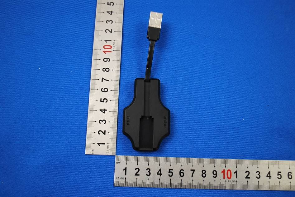
QVY53P
Dec 27, 2012Strapless continuous heart rate monitor
Equipment Class
DTS - Digital Transmission System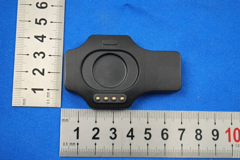
QVY52P
Dec 09, 2012Strapless continuous heart rate monitor
Equipment Class
DXX - Part 15 Low Power Communication Device Transmitter