RF6-NACO17ALCD Monitor
All In One Display.Inc.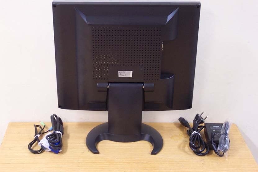
Click to zoom
Application Details
- Equipment Class
- JBP - Part 15 Class B Computing Device Peripheral
- Date of Grant
- Oct 01, 2003
- Application Purpose
- Original Equipment
- Date of Application
- Oct 01, 2003
- Equipment Note
- LCD Monitor
- Company
- All In One Display.Inc.
- Country
- South Korea
Documents & Files
Document Text
Text extracted from the exhibit documents filed with the FCC. Open a document above to read the original.
Block Diagram
17”LCD Block Diagram Audio out Audio in Video in TTL LVDS 12V 5V 3.3V Scaler LVDS Tx Flash 24C16 DC/DC DC/DC DC/DC Inverter 2.5V blacklight Panel Audio amplifier
Cover Letter(s)
1 Mike Kuo From:[email protected] Sent:October062003Monday 5:31 PM To:Mike Kuo Subject:Re: ALL IN ONE SEMICONDUCTOR INC., FCC ID:RF6-NACO17A, AN03T3232 03-341-029(Class B)-Revised 2n... Dear Mr. Mike Kuo, According to your configuration, we retested LCD Minitor. (One serial mouse is added.) Thank you for your correction. And please please consider my client's urgent situation. Best rergards. Deog-Soo Ko ==================================== Korea Testing Laboratory Information & Telecommunication Team Tel:02-860-1464 Fax:02-860-1468 ==================================== ----- Original Message ----- From: "Mike Kuo" <[email protected]> To: "'???'" <[email protected]> Sent: Friday, October 03, 2003 7:24 AM Subject: RE: ALL IN ONE SEMICONDUCTOR INC., FCC ID:RF6-NACO17A, AN03T3232 > Hi Deog-Soo: > > Based upon the review of the revised test report, the test configuration > still does not comply with ANSI C63.4 section 11.2 requirement. Mouse and > Keyboard do not consider to meet the at least two different I/O protocols > requirements. The keyboard and mouse you are using are with PS/2 interface > which are dedicated to keyboard and mouse. You only use one additional > Parallel port ( printer ) during the tests. Suggested configuration : > > Video display ( EUT ) + PS/2 Mouse + PS/2 Keyboard + Host PC + HP parallel > printer + Serial Mouse or Serial Modem. > > Please redo the tests with above suggested test configuration and submit the > test report. > > Best Regards > > Mike Kuo > > -----Original Message----- > From: [email protected] [mailto:[email protected]] > Sent: Wednesday, September 17, 2003 12:36 AM > To: Mike Kuo > Subject: Re: ALL IN ONE SEMICONDUCTOR INC., FCC ID:RF6-NACO17A, > AN03T3232 2 > > > Dear Mike Kuo, > > How are you? > > Above all, I'm sorry for my negligence in preparing test reports. > > I have re-tested the monitor under the worst 1280x1024 resolution > mode according to your notice.(See the attached re-test report.) > > Your questions are > > Question #1: Per the description in the user manual, this monitor is capable > of generating 1280x1024 resolution. In the test report, there is no place > to indicate which resolution was tested. Please provide detail information > what is the worst resolution during the final compliance tests. > > Answer : Pls. see page 6 of attached test report. > (The former report you have is under the 1024x768 resolution mode.) > > > Question #2: Page 3 of test report listed the support equipment used during > the final compliance tests. Since there is not description on the type of > interface for each support equipment, the radiated and conducted emission > tests may not comply with ANSI C63.4 section 11.2 which require at least two > different protocols during the tests. Based upon the support > equipment list, only one protocol was connected ( printer ). Please explain > the type of interface for each support equipment or redo the tests per ANSI > C63.4 section 11.2 requirement. > > Answer : Pls. see page 3 of attached test report. > > Question #3: Please list the type of cable that was used during the final > compliance tests including ferrite core information for each cable. In the > future filing, please take a test setup photo to show all the > inter-connecting cables. > > Answer : Pls. see page 3 of attached test report. > > We will keep in mind your notice in the future tests. > > I hope this answer will be helpful in your quick handling our client's > application. > Best regards. > > Deog-Soo Ko > P.S. : The data of CE, RE test under 1280x1024 resolution mode > replaced the previous(1024x768) one. > > ==================================== > Korea Testing Laboratory > Information & Telecommunication Team > Tel:02-860-1464 Fax:02-860-1468 > ==================================== > ----- Original Message ----- > From: "Mike Kuo" <[email protected]> > To: "'???'" <[email protected]> > Sent: Tuesday, September 16, 2003 8:11 AM > Subject: FW: ALL IN ONE SEMICONDUCTOR INC., FCC ID:RF6-NACO17A, AN03T3232 > > > > 3 > > > > -----Original Message----- > > From: CERTADM > > Sent: Monday, September 15, 2003 4:10 PM > > To: '[email protected]' > > Subject: ALL IN ONE SEMICONDUCTOR INC., FCC ID:RF6-NACO17A, AN03T3232 > > > > > > Notice_content > > ------------- > > Question #1: Per the description in the user manual, this monitor is > capable > > of generating 1280x1024 resolution. In the test report, there is no > place > > to indicate which resolution was tested. Please provide detail > information > > what is the worst resolution during the final compliance tests. > > > > Question #2: Page 3 of test report listed the support equipment used > during > > the final compliance tests. Since there is not description on the type of > > interface for each support equipment, the radiated and conducted emission > > tests may not comply with ANSI C63.4 section 11.2 which require at least > two > > different protocols during the tests. Based upon the support > > equipment list, only one protocol was connected ( printer ). Please > explain > > the type of interface for each support equipment or redo the tests per > ANSI > > C63.4 section 11.2 requirement. > > > > Question #3: Please list the type of cable that was used during the final > > compliance tests including ferrite core information for each cable. In > the > > future filing, please take a test setup photo to show all the > > inter-connecting cables. > > > > For your information, schematic diagram is not required for Personal > > computer and peripheral device. > > > > Best Regards > > > > Mike Kuo > > > > The items indicated above must be submitted before processing can continue > > on the above referenced application. Failure to provide the requested > > information within 30 days of the original e-mail date may result in > > application dismissal and forfeiture of the filing fee. Also, please note > > that partial responses increase processing time and should not be > submitted. > > Any questions about …
Text truncated - open the document above for the full version.
External Photos
External Photo (Front Side) (Rear Side)
Test Report
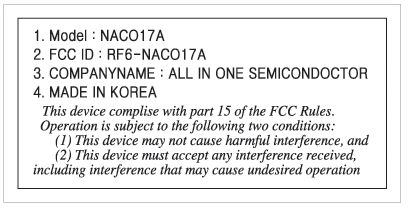
R No. 03 - 341 – 004ef. Report Page 1 of 13 Korea Testing Laboratory Page 1 of 13 Ref. Report No. Name and address of the applicant ALL IN ONE SEMICONDUCTOR. INC. Rm 305, Jiovil Officetel., 122-3, Yeonhee-Dong, Seodaemoon-Ku, Seoul, Korea Standard / Test regulation FCC Part 15, Subpart B Test result Pass Incoming date : Aug. 28, 2003 Test item(s) ; Class B PC & Peripherals (LCD Monitor) Model/type ref. ; NACO17A Manufacturer ; Day System Co., Ltd. Additional information ; -Required Authorization : Certification -FCC ID. : RF6-NACO17A Test date : Oct. 6, 2003 Issue date : Oct. 7, 2003 This test report only responds to the tested sample and shall not be reproduced except in full without written approval of the Korea Testing Laboratory. Tested and reported by Reviewed by Deog-Soo Ko, Senior Engineer Hee-Soo Kim , Telecommunication Team Manager FG101-01-02-00 222-13, Guro-Dong Guro-Gu Seoul Korea 152-848 http://www.ktl.re.kr Ref. Report No. 03 - 341 - 029 Page 2 of 13 TABLE OF CONTENTS I. GENERAL INFORMATION 3 1. Applicant’s Name and Mailing Address 2. Manufacturer's Name and Mailing Address 3. Equipment Descriptions 4. Rules and Regulations 5. Measuring Procedure 6. Date of Measurement . GENERAL REQUIREMENTS OF THE EUT 4 1. Labeling Requirement (Section 15.19) 2. Information to User (Sections 15.21and 15.105) 3. Special Accessories (Section 15.27) . CONDUCTED EMISSION MEASUREMENT (Section 15.107) 6 1. Test Procedure 2. Photograph for the test configuration 3. Sample Calculation 4. Measurement Data . RADIATED EMISSION MEASUREMENT (Section 15.109) 10 1. Test Procedure 2. Photograph for the test configuration 3. Sample Calculation 4. Measurement Data . TEST EQUIPMENTS USED FOR MEASUREMENT 13 Korea Testing Laboratory Telecommunication Team 222-13, Guro3-dong, Guro-gu, Seoul Korea 152-848 Ref. Report No. 03 - 341 - 029 Page 3 of 13 . GENERAL INFORMATION 1. Applicant’s Name and : ALL IN ONE SEMICONDUCTOR. INC. Mailing Address Rm 305, Jiovil Officetel., 122-3, Yeonhee-Dong, Seodaemoon-Ku, Seoul, Korea 2. Manufacturer's Name and : Day System Co., Ltd. Mailing Address 459-21, Gasan-Dong, Gumchun-Ku, Seoul, Korea 3. Equipment Descriptions 3.1 Crystal used : 14.318180 MHz, (Utech Industrial Co., Ltd.) 3.2 Power Supply : DC 12V 4.3A - Power Adapter used for testing : SAD5012SE (Input : AC100-240V, 50/60Hz), DC 12 V 4.3A (Seronics Co., Ltd.) 3.3 Auxiliary Equipment : Personal Computer (DPEP P500, Compaq) Mouse (M-S34, Compaq, PS/2) Mouse (?? Serial Port) Keyboard (RT235BTWKO, Compaq, PS/2) Printer (2225C+, H/P, Parallel port) 3.4 Used cable type list : Mouse cable (Fixed, Unshielded, 1.5m*2) Keyboard cable (Fixed, Unshielded, 1.5m) Monitor cable (Unshielded, 1.5m, with fixed ferrite cores at both ends of the cable) Printer cable (Unshielded, 1.5m) 4. Rules and Regulations : FCC Part 15, Subpart B 5. Measuring Procedure : ANSI C63.4-2001 6. Date of Measurement 6.1 Conducted Emission : Oct. 6, 2003 6.2 Radiated Emission : Oct. 6, 2003 Korea Testing Laboratory Telecommunication Team 222-13, Guro3-dong, Guro-gu, Seoul Korea 152-848 Ref. Report No. 03 - 341 - 029 Page 4 of 13 . GENERAL REQUIREMENTS OF THE EUT 1. Labeling Requirement (Section 15.19) This device complies with Part 15 of the FCC Rules. Operation is subject to the following two conditions: (1) this device may not cause harmful interference, and (2) this device must accept any interference received, including interference that may cause undesired operation. 1.1 Location of Label : Label & User’s Guide Manual 1.2 How Applied : Printed 2. Information to User (Section 15.21 and 15.105) The following or similar statements were provided in the manual for user instruction. Please refer page 2 of the attached manual for details. CAUTION : Any changes or modifications in construction of this device which are not expressly approved by the party responsible for compliance could void the user's authority to operate the equipment. Note : This equipment has been tested and found to comply with the limits for a Class B digital device, pursuant to part 15 of the FCC Rules. These limits are designed to provide reasonable protection against harmful interference in a residential installation. This equipment generates, uses and can radiate radio frequency energy and, if not installed and used in accordance with the instructions, may cause harmful interference to radio communications. However, there is no guarantee that interference will not occur in a particular installation. If this equipment does cause harmful interference to radio or television reception, which can be determined by turning the equipment off and on, the user is encouraged to try to correct the interference by one or more of the following measures: - Reorient or relocate the receiving antenna. - Increase the separation between the equipment and receiver. - Connect the equipment into an outlet on a circuit different from that to which the receiver is connected. - Consult the dealer or an experienced radio/TV technician for help. Korea Testing Laboratory Telecommunication Team 222-13, Guro3-dong, Guro-gu, Seoul Korea 152-848 Ref. Report No. 03 - 341 - 029 Page 5 of 13 3. Special Accessories (Section 15.27) 3.1 Were the special Accessories provided? [ ] yes, [ x ] no 3.2 If yes, details for the special accessories are as follows : 3.3 If yes, were the appropriate instructions provided on the first page of the text concerned with the device? [ ] yes, [ ] no 3.4 Are these accessories provided of the type which can be readily obtained from multiple retail outlets ? [ ] yes, [ ] no And therefore does the manual specify what additional components or accessories are required to used in order to comply with the Rules? [ ] yes, [ ] no Korea Testing Laboratory Telecommunication Team 222-13, Guro3-dong, Guro-gu, Seoul Korea 152-848 Ref. Report No. 03 - 341 - 029 Page 6 of 13 . CONDUCTED EMISSION MEASUREMENT (Section 15.107) 1. Test Procedure Conducted emission measurements on the EUT were performed by "AC Powe…
Text truncated - open the document above for the full version.
Test Setup Photos
Ref. Report No. 03 - 341 - 029 Page 7 of 13 2. Photograph for the test configuration 3. Sample Calculation The emission level measured in decibels above one microvolt (dB) was converted into microvolt () as shown in following sample calculation. For example : Measured Value at 6.30 MHz 37.3 dB@ Q-peak mode + Cable Losses * 0.0 dB = Conducted Emission 37.3 dB ( = 73.28 ) * In case of RG214/RF cable 15 Ft, the loss is about 0.17 dB at the frequency of 30 MHz which is negligible. Korea Testing Laboratory Telecommunication Team 222-13, Guro3-dong, Guro-gu, Seoul Korea 152-848 Ref. Report No. 03 - 341 - 029 Page 11 of 13 2. Photograph for the test configuration 3. Sample Calculation The emission level measured in decibels above one microvolt (dB) was converted into microvolt per meter (/m) as shown in following sample calculation. For example : Measured Value at 84.01 MHz 21.3 dB + Antenna Factor 8.2 dB/m + Cable Loss 1.6 dB Preamplifier 0.0 dB Distance Correction Factor * 0.0 dB -------------------------------------------------------------------------------- = Radiated Emission 31.1 dB/m ( = 35.9 /m ) * Extrapolated from the measured distance to the specified distance by an inverse linear distance extrapolation. Korea Testing Laboratory Telecommunication Team 222-13, Guro3-dong, Guro-gu, Seoul Korea 152-848
Contact Information
Applicant
Ji-Hong Jung(Deputy General Manager)
Test Firm
Korea Testing LaboratoryJeong-Min Kim
Technical Specifications
| # | Rule Parts | Frequency Range | Power Output |
|---|---|---|---|
| 1 | 15B | - | - |
Other Applications from All In One Display.Inc.
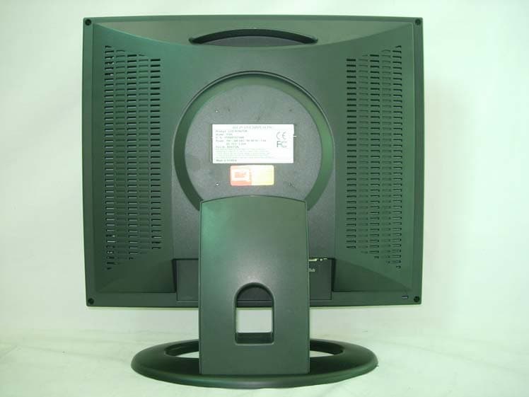
RF6172N
Nov 10, 2005LCD Monitor
Equipment Class
JBP - Part 15 Class B Computing Device Peripheral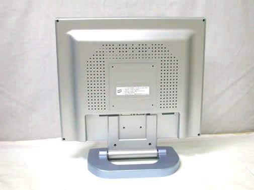
RF6NACO170D
Aug 15, 2004TFT-LCD Monitor
Equipment Class
JBP - Part 15 Class B Computing Device Peripheral