RUNZT3Zigbee Data Device
Freescale Semiconductor, Inc.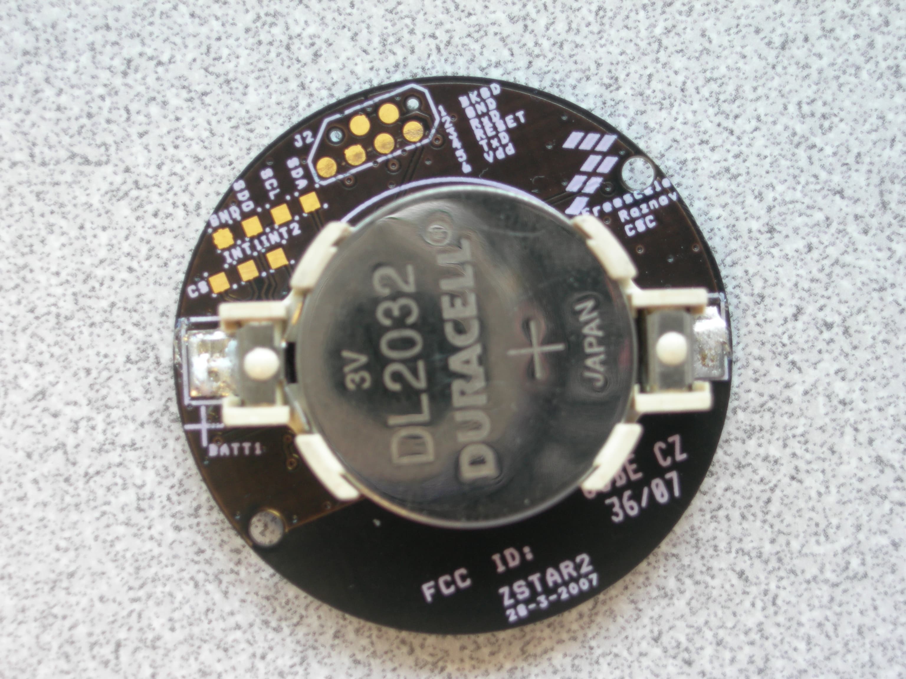
Click to zoom
Application Details
- Equipment Class
- DTS - Digital Transmission System
- Date of Grant
- Apr 06, 2008
- Application Purpose
- Original Equipment
- Date of Application
- Apr 03, 2008
- Equipment Note
- Zigbee Data Device
- Frequency Range
- 2405.00000000 - 2480.00000000
- Country
- United States
Documents & Files
Document Text
Text extracted from the exhibit documents filed with the FCC. Open a document above to read the original.
Users Manual
freescale.com ZStar3 Multiple Wireless Sensing Triple Axis Reference Design ZSTAR3RM Rev. 0 01/2008 Safety of Radio Frequency Energy The manufacturer has evaluated the transmitter for safe operation for uncontrolled use in the general population. The measured power density at 1 cm is under the threshold established by the FCC and is not required to be tested for specific absorption rate. The manufacturer instructs the user that the transmitter should not be handled or placed near the body continuously for more than 30 minutes while operating. USA: NOTE: This equipment has been tested and found to comply with the limits for a Class B digital device, pursuant to Part 15 of the FCC Rules. These limits are designed to provide reasonable protection against harmful interference in a residential installation. This equipment generates, uses and can radiate radio frequency energy and, if not installed and used in accordance with the instructions, may cause harmful interference to radio communications. However, there is no guarantee that interference will not occur in a particular installation. If this equipment does cause harmful interference to radio or television reception, which can be determined by turning the equipment off and on, the user is encouraged to try to correct the interference by one or more of the following measures: – Reorient or relocate the receiving antenna. – Increase the separation between the equipment and receiver. – Connect the equipment into an outlet on a circuit different from that to which the receiver is connected. – Consult the dealer or an experienced radio/TV technician for help. This device complies with Part 15 of the FCC Rules. Operation is subject to the following two conditions: (1) this device may not cause harmful interference, and (2) this device must accept any interference received, including interference that may cause undesired operation. Changes or modifications not expressly approved by the party responsible for compliance could void the user's authority to operate the equipment. The antenna(s) used for this transmitter must not be co-located or operating in conjunction with any other antenna or transmitter. Canada: This digital apparatus complies with Canadian ICES-003. Cet appareil numérique est conforme à la norme NMB-003 du Canada. Europe: Compliant (CE) Rev. 0 01/2008 <<Title>> Freescale Semiconductor<Red>Freescale Internal Use Only-3 <<Status>> Contents Introduction 7 Introduction 7 ZSTAR3 Wireless Sensing Triple Axis Reference design Introduction 9 Introduction 9 Features of ZSTAR3 10 Featured Products 11 Triple Axis Analogue Accelerometer MMA7360L 11 Triple Axis Digital Accelerometer MMA7450L 11 The SiP(System in Package) MC13213 12 ZSTAR3 Sensor Board Description 15 Board Overview 15 Accelerometric sensor sw controller 17 Double sensor support software model 17 Autocalibration process 17 Analogue sensor software support 18 Digital sensor software support 18 Power Management 18 MC13213 Modem Power Management Features 20 ZSTAR Sensor Board Hardware Overview 20 Sensors power supply 21 Analogue sensor connection 21 Digital sensor connection 21 BDM (Background Debug Mode) Connections 21 Button Connections 22 MC13213 RF Interface 22 Clocking Options of MC9S08QG8 23 LED Indicator 23 Power Supply 23 Bill of Materials 24 ZSTAR3 schematic 26 USB stick Board Description 29 Board Overview 29 Software Design 31 Introduction 31 SMAC (Simple Media Access Controller) 31 SMAC Features 31 <<Title>> -4<Red>Freescale Internal Use OnlyFreescale Semiconductor <<Status>> Modifications of SMAC for ZSTAR3 RF protocol 31 New targets add to SMAC 32 New functions add to SMAC 32 ZSTAR3 RF Protocol 32 ZSTAR3 RF protocol features 32 Zpacket Format 33 Network Number(NetNum) 34 RX Strength 34 Zcommand 34 Zdata 35 Original ZSTAR Zcommand Description 35 ZSTAR3 Protocol Zcommand Description 35 ZSTAR3_PYLON 36 ZSTAR3_DATA 36 ZSTAR3_ACK 36 ZSTAR3_CONNECT 36 ZSTAR3_ION 36 ZSTAR3 Protocol SubCommands Description 36 ZSTAR3_GUI 36 ZSTAR3_MODE 37 ZSTAR3_OFF 37 ZSTAR3_GSEL 37 ZSTAR3_DATARATE 37 ZSTAR3_FLAG 37 ZSTAR3 RF Protocol description 37 Typical one period of ZSTAR3 RF protocol 38 ZSTAR3 USB protocol - Extended STAR protocol 39 Subset of original STAR protocol commands 39 Subset of original ZSTAR protocol commands 40 Subset of new added ZSTAR3 protocol commands 41 Burst mode 43 Network Lock feature of ZSTAR3 protocol 43 Semiautomatic Self-Calibration 43 Compatiblity with Original ZSTAR 44 Bootloader 44 Switch to Bootloader procedure 44 Bootloading Procedure 45 Triapplication software of USB Stick 48 CDC - Virtual Serial Port application 48 HID - Mouse application 48 HID - Keyboard application 48 Applications Switching 49 Application Setup 51 ZSTAR3 Installation Procedure 51 <<Title>> Freescale Semiconductor<Red>Freescale Internal Use Only-5 <<Status>> USB stick Installation 51 AN2295 Bootloader Drivers installation 55 ZSTAR3 GUI 59 Installation 59 ZSTAR3 GUI 62 Features of ZSTAR GUI 62 The ZStar3 GUI main controls 63 USB Data Flow monitor 63 Sensor Board overview screen 64 RF overview screen 65 General sensor tasks 66 Scope demo application 67 Acquire data demo application 68 Tilt tasks 69 Filtered tilt demo application 70 Motion tasks 71 Position tasks 72 Shock tasks 73 Digital tasks 74 Sensor registers demo application 75 Freescale Web Links. 76 The ZStar3 GUI Update USB Stick Software utility 76 Update process (Manual start) 77 References 81 <<Title>> -6<Red>Freescale Internal Use OnlyFreescale Semiconductor <<Status>> Introduction ZSTAR3 Reference Design Manual, Rev. 0.1 Freescale SemiconductorFreescale Confidential Proprietary 1-7 Freescale Internal Use Only Preliminary Pr e l i m i n a ry Chapter 1 Introduction 1.1Introduction This paper describes the next generation of design of a Wireless Sensing Triple Axis Reference design (ZSTAR3), a demo for wireless demonstration of the 3-axes accelerometers MMA7450L (RD3172MMA7450L) and MMA7360L (RD3172MMA7360L) sensors from Freesc…
Text truncated - open the document above for the full version.
Block Diagram
55 44 33 22 11 D D C C B B A A XTAL2XTAL1 Antenna XTAL1XTAL2 RESET TXDRXD BDM Z-axisY-axisX-axisSLEEP X-axisY-axisZ-axis X-axis 0g_detect self_testg-selectSLEEP self_test INT1SDOSCL/SPC SCL/SPC Y-axis Z-axis switch1 SDO switch3switch2 INT1 0g_detect g-select SDO self_testSCL/SPC g-select GND GND GND GND GND GND GND VDD VDD GND GND GND GND GND GND GND VDD VDD GND GND GND GND GND GND VDD GND GND GND RXDTXDRESETBDM LED1 LED1 Title Size Design Name: Rev Modify Date: Sheet of Schematic Name:Copyright Freescale POPI Status: Author: 0 ZSTAR2 Freescale Semiconductor Roznov CSC1. maje 1009756 61 Roznov p.R., Czech Republic, Europe A4 11 Tuesday, March 20, 2007 SCHEMATIC1 General Business Information <Author> 2005 D:\CCWORK\B01119_VIEW_DEV\ICONN\IC116 - ZSTAR2 - LOW-COST 2.4GHZ AND X Title Size Design Name: Rev Modify Date: Sheet of Schematic Name:Copyright Freescale POPI Status: Author: 0 ZSTAR2 Freescale Semiconductor Roznov CSC1. maje 1009756 61 Roznov p.R., Czech Republic, Europe A4 11 Tuesday, March 20, 2007 SCHEMATIC1 General Business Information <Author> 2005 D:\CCWORK\B01119_VIEW_DEV\ICONN\IC116 - ZSTAR2 - LOW-COST 2.4GHZ AND X Title Size Design Name: Rev Modify Date: Sheet of Schematic Name:Copyright Freescale POPI Status: Author: 0 ZSTAR2 Freescale Semiconductor Roznov CSC1. maje 1009756 61 Roznov p.R., Czech Republic, Europe A4 11 Tuesday, March 20, 2007 SCHEMATIC1 General Business Information <Author> 2005 D:\CCWORK\B01119_VIEW_DEV\ICONN\IC116 - ZSTAR2 - LOW-COST 2.4GHZ AND X BDM SENSOR LED MCU + RF POWER SOURCE CLOCK SOURCE SCLSCL 1 SDASDA 1 BATT1 Battery/Renata CR2032 BATT1 Battery/Renata CR2032 L14.7nHL14.7nH J2BDMJ2BDM 12 34 65 C1310nFC1310nF R1470RR1470R C410nFC410nF D1LEDD1LED C5100nFC5100nF C126.8PFC126.8PF MCU_CLKMCU_CLK 1 C2 6.8PF C2 6.8PF C3 6.8PF C3 6.8PF L322nHL322nH C111uFC111uF L222nHL222nH C1410nFC1410nF C1510nFC1510nF S2 Alps SKRP S2 Alps SKRP 1 34 2 C10100nFC10100nF C7100nFC7100nF + C1100uF/4V + C1100uF/4V 12 R20R - IONR20R - ION S1 Alps SKRP S1 Alps SKRP 1 34 2 C9100nFC9100nF C6100nFC6100nF X116MHz NX2520SAX116MHz NX2520SA 12 34 SDOSDO 1 S3 Alps SKRP S3 Alps SKRP 1 34 2 C8100nFC8100nF U2MERCURY/IONU2MERCURY/ION VDD,AVdd 6 VSS,GND 5 Xout,NC 2 Yout,NC 3 Zout,GND 4 0g - detect,INT2 9 Self_test,SDA/SDI/SDO 13 g-select, GND 10 Sleep, CS 7 NC, DVdd_IO 1 NC, INT1/DRDY 8 NC, NC 11 NC, SDO 12 NC,SCL/SPC 14 U1MC13211U1MC13211 PTE0/TxD1 20 PTA3/KBD3 1 VREFH 60 VREFL 61 PTA0/KBD0 62 PTA1/KBD1 63 PTA2/KBD2 64 PTC6 18 PTC7 19 PTE1/RxD1 21 PTA4/KBD4 2 PTA5/KBD5 3 PTA6/KBD6 4 PTA7/KBD7 5 VDDAD 6 CLKOo 10 PTG0/BKGD/MS 7 PTG1/XTAL 8 PTG2/EXTAL 9 RESET 11 PTC0/TxD2 12 PTC1/RxD2 13 PTC2/SDA 14 PTC3/SCL 15 PTC4 16 PTC5 17 XTAL2 28 VDDLO2 29 VDDLO1 30 VDDVCO 31 VBATT 32 VDDA 33 CT_Bias 34 RFIN_M 35 PTB0/AD0 52 PTB1/AD1 53 PTB2/AD2 54 PTB3/AD3 55 PTB4/AD4 56 PTB5/AD5 57 PTB6/AD6 58 PTB7/AD7 59 GPIO1 44 VDD 45 ATNBi 46 PTD2 47 PTD4 48 PTD5 49 PTD6 50 PTD7 51 RFIN_P 36 TINJ_M 37 PAO_P 38 PAO_M 39 SM 40 GPIO4 41 GPIO3 42 GPIO2 43 GPIO5 24 GPIO6 25 GPIO7 26 XTAL1 27 VDDINT 23 VDDD 22 PTE5/SPICLK 65 PTE4/MOSIi 66 PTE3/MISOo 67 PTE2/CEBi 68 IRQ/IRQo 69 PTD1/RXTXENi 70 PTD3/RSTBi 71 Exposed Pad 72
Cover Letter(s)
NOTE REGARDING CONFIDENTIALITY.doc Page 1 of 1 Regarding FCC ID RUNZT3 This note confirms that confidentiality is not requested for this application. The client wishes the documentation to be available to share with their customers as this is an engineering evaluation product. ***
Cover Letter(s)
American Telecommunications Certification Body Inc. 6731 Whittier Ave, McLean, VA 22101 March 31, 2008 RE: FCC ID: RUNZT3_ATCB006078 Attention: Michael Royer / Jason Anderson I have a few comments on this Application. Please note that further comments may arise in response to answers provided to the questions below. 1. Please note that the FCC ID labeling shown on the device is not the same as that provided in the label exhibit. Please note that the FCC requires that the entire FCC ID number, including the prefix FCC ID: is to be on a single line. Please note that the FCC ID number shown on the device is on two separate lines. Please correct and make sure that the FCC ID number is on a single line as is shown in the label exhibit. 2. The Internal photos do not show both sides of the device, but only show on side with the plastic battery housing attached and the same side with the plastic battery housing taken off. Please explain and please provide appropriate internal photos. 3. Please note that only modules and end products are certified. Please note that unless this is an application for a modular approval, the device must be housed in a ‘box’ or other end product housing. If this is a modular approval, then please provide the necessary modular approval request letter addressing all 8 modular approval criteria. If this is not a modular approval, please test the device inside a typical housing. 4. Please note that the test report does not clearly state what approved FCC test procedure was used to test the device. Please note that as this is a DSSS type device the appropriate approved test procedure would be the FCC DTS test procedure found in KDB558074. Please confirm that this test procedure was used and please make reference to this test procedure in the test report. 5. Please note that in calculating the EIRP of the device you apparently used an antenna gain of 0dBi. Please note that there is no documentation to support this gain. As the G (gain) used in the formula (Ed)^2/30G is the gain of the antenna, it is necessary to show what the actual gain of the antenna is before using the formula. Please note that this also applies to the PPSD data. Please note that it cannot simply be assumed that the gain is 0dBi. Please provide the antenna gain information for the device antenna or please provide actual conducted power measurements and power spectral density measurements at the antenna terminal. 6. Please note that for radiated spurious emissions in the restricted bands, while duty cycle averaging may be allowed for pulsed devices (typically allowed for FHSS type devices), it is not allowed for non-pulsed devices. Please adequately show how this device is to be considered a pulsed device whereby the 100ms pulse duty cycle correction of 15.35 may be used. Please also note that pulse modulation involves modulating a carrier with a train of regularly recurrent pulses . Please note that a direct sequence spread spectrum device does not use a series of regularly recurrent pulses, but uses a pseudo random transmission scheme. If this is a pulsed transmission, please not only adequately explain how the device is a DSSS and generates regularly recurrent pulses and please show the plots over 100ms in accordance with 15.35(b)(c). Please adequately show the duty cycle calculations involved in the method. If it cannot be shown how this is a pulsed transmission (i.e. it is not a set of regularly recurrent pulses - please note that simply being direct sequence spread spectrum device tends to not mean pulsed emission), then you must use the accepted averaging methods shown in the FCC accepted test procedures found in KDB558074 using a res Bw of 1MHz and a vid bandwidth or 10Hz etc. Please provide appropriate average data in accordance with the accepted test procedures. 7. Please note that in the radiated spurious emissions tables you state that at 1 meter the limits are 83.4dBuV/m average. Please note that this is not accurate. Please note that at 4810MHz and 4880MHz ( both in the restricted bands) the average limit at 3 meters is 54dBuV/m. This means that at 1 meter the restricted band limit at 4810MHz would be 64dVuV/m (i.e. 20 dB/decade or 20log 3/1). Please note that this also means that the device apparently fails at 4810 and z Page 2 March 31, 2008 4880MHz. Please retest using the appropriate restricted band limits and the appropriate and approved averaging method per the KDB. 8. Please review your data and make sure that all data is passing and in compliance with the accepted test procedures for this type device. 9. Please provide an adequate operational description for this device. 10. Please note that further comments may arise depending on the response to the above. Dennis Ward mailto:[email protected] The items indicated above must be submitted before processing can continue on the above referenced application. Failure to provide the requested information may result in application termination. Correspondence should be considered part of the permanent submission and may be viewed from the Internet after a Grant of Equipment Authorization is issued. Please do not respond to this correspondence using the email reply button. In order for your response to be processed expeditiously, you must submit your documents through the AmericanTCB.com website. Also, please note that partial responses increase processing time and should not be submitted. Any questions about the content of this correspondence should be directed to the sender.
Cover Letter(s)
dward From: Mike Urban (Home2) [[email protected]] Sent: 04/04/2008 2:10 PM To: 'Dennis Ward' Cc: [email protected] Subject: FW: test 04/04/08 From: Mike Royer [mailto:[email protected]] Sent: Friday, April 04, 2008 5:07 PM To: [email protected] Subject: test I get errors on reply mail to [email protected]. Where should I send my replies? Best regards, Mike Hello Dennis, Thank you for your comments and help. Here is our reply to your comments; 1. You are correct that the silkscreen in the prototype photographed is on two lines and is missing the IC number. Freescale will have the production revision match the label drawing submitted. If needed, an attestation to this effect could be produced. 2.The photo of the other side of the board is located under external photos. It is DSCN2303.JPG. 3.This is an end product. It is an evaluation kit for learning to use Freescale semiconductor products. This was allowed for FCC ID: RUNZT. 4.Huh? Where can we find this procedure? Why was our format suitable for RUNZT? 5.0 dbi is the worst case antenna gain. We assume that the antenna is not truly isotropic or 100% efficient. If we assumed that the antenna has 2 dBi gain, then we would be allowed 2 dB more signal at the range receive antenna. Considering that we are 30 dB below the limits, 0 dBi is a good assumption. 6.This is a pulsed product with a train of regularly recurrent pulses. Each pulse contains accelerometer information, and is accompanied by an acknowledgement pulse from the USB stick companion device. Additionally, within each pulse DSSS is used. This is typical of Zigbee protocols, yes? 7.We used the 20 dB calculated relaxation for pulsed signals against the limit. We have amended the report to show the peak and average signals against a limit of 63.5 dBuV/m at 1m. 8. Done. 9. We will upload an operational description. 10. Granted. Best regards, Mike From: dward [mailto:[email protected]] Sent: Monday, March 31, 2008 1:58 PM To: [email protected]; [email protected] Cc: [email protected] Subject: www.AmericanTCB.com ATCB006078 | RUNZT3 | 6744A - ZT3 | | RUNZT3_ATCB006078 Regarding www.AmericanTCB.com application: ATCB ID: ATCB006078 FCC ID: RUNZT3 IC: 6744A - ZT3 TCF: Account name: Nikki HI Mike Please see comments Thanks Dennis 04/04/08
ID Label/Location Info
Label Art Rev 1.doc Page 1 of 1 FCC ID: RUNZT3 IC: 6744A-ZT3 (Embedded into silk screen.)
Operational Description
This is one device of a paired transceiver set, one a USB key/stick, the other a battery operated wireless sensor board. This set functions as an engineering demonstration of the Freescale chip set technology and is not intended for final use applications. The Sensor board (EUT) is an independent battery-operated wireless XYZ accelerometer sensor. When switched on it seeks out its companion USB Key, connects and streams continuous accelerometer readings to a demo program on the host PC. The EUT is a dual-layer printed circuit board. It contains the basic design of the MC13191 RF transceiver implementing the ZigBee protocols and is connected through an 8-bit MC9S08QG8 microcontroller to the MMA7260Q accelerometer sensor chip. Its sole task is to send data from the MMA7260Q accelerometer via the MC1311 using ZigBee protocols to the companion USB Key ZigBee radio.
RF Exposure Info
FCC RF Exposure Rev 2.doc Page 1 of 1 Radio Frequency exposure was evaluated on the EUT to determine compliance with FCC 15.247(b)(5) and RSS-210. The FRIIS transmission formula was applied to the peak power measurements obtained in section 2 of the test report. FCC 1.1307(b) cites the limits for maximum permissible exposure (MPE) from 1.1310 and must be used to evaluate the impact of human exposure to radio frequency energy. The limits from 1.1310 are listed below: Frequency MHz Power Density (mW/cm²) Average Time (Minutes) Limits for Occupational / Controlled Exposures 30-300 1.0 6 300-1500 f/300 6 1500-100,000 5 6 Limits for General Population / Uncontrolled Exposures 30-300 0.2 30 300-1500 f/1500 30 1500-100,000 1.0 30 2 **4 * r GP tyPowerDensi t π = Exposure Frequency (MHz) Calculated EIRP Power (dBm) Linear Power (mW) Distance (cm) Power Density (mW/cm 2 ) Limit (mW/cm 2 ) 2405 -17.4 0.018 1 0.0163 1.0 Result: The EUT meets the Maximum Permissible Exposure Limits. SAR Threshold Assessment Frequency (MHz) Power Density (mW/cm 2 ) SAR Threshold mW 2405 0.0163 24.56 Result: The EUT power density is below the SAR threshold. ***
Schematics
55 44 33 22 11 D D C C B B A A XTAL2XTAL1 Antenna XTAL1XTAL2 RESET TXDRXD BDM Z-axisY-axisX-axisSLEEP X-axisY-axisZ-axis X-axis 0g_detect self_testg-selectSLEEP self_test INT1SDOSCL/SPC SCL/SPC Y-axis Z-axis switch1 SDO switch3switch2 INT1 0g_detect g-select SDO self_testSCL/SPC g-select GND GND GND GND GND GND GND VDD VDD GND GND GND GND GND GND GND VDD VDD GND GND GND GND GND GND VDD GND GND GND RXDTXDRESETBDM LED1 LED1 Title Size Design Name: Rev Modify Date: Sheet of Schematic Name:Copyright Freescale POPI Status: Author: 0 ZSTAR2 Freescale Semiconductor Roznov CSC1. maje 1009756 61 Roznov p.R., Czech Republic, Europe A4 11 Tuesday, March 20, 2007 SCHEMATIC1 General Business Information <Author> 2005 D:\CCWORK\B01119_VIEW_DEV\ICONN\IC116 - ZSTAR2 - LOW-COST 2.4GHZ AND X Title Size Design Name: Rev Modify Date: Sheet of Schematic Name:Copyright Freescale POPI Status: Author: 0 ZSTAR2 Freescale Semiconductor Roznov CSC1. maje 1009756 61 Roznov p.R., Czech Republic, Europe A4 11 Tuesday, March 20, 2007 SCHEMATIC1 General Business Information <Author> 2005 D:\CCWORK\B01119_VIEW_DEV\ICONN\IC116 - ZSTAR2 - LOW-COST 2.4GHZ AND X Title Size Design Name: Rev Modify Date: Sheet of Schematic Name:Copyright Freescale POPI Status: Author: 0 ZSTAR2 Freescale Semiconductor Roznov CSC1. maje 1009756 61 Roznov p.R., Czech Republic, Europe A4 11 Tuesday, March 20, 2007 SCHEMATIC1 General Business Information <Author> 2005 D:\CCWORK\B01119_VIEW_DEV\ICONN\IC116 - ZSTAR2 - LOW-COST 2.4GHZ AND X BDM SENSOR LED MCU + RF POWER SOURCE CLOCK SOURCE SCLSCL 1 SDASDA 1 BATT1 Battery/Renata CR2032 BATT1 Battery/Renata CR2032 L14.7nHL14.7nH J2BDMJ2BDM 12 34 65 C1310nFC1310nF R1470RR1470R C410nFC410nF D1LEDD1LED C5100nFC5100nF C126.8PFC126.8PF MCU_CLKMCU_CLK 1 C2 6.8PF C2 6.8PF C3 6.8PF C3 6.8PF L322nHL322nH C111uFC111uF L222nHL222nH C1410nFC1410nF C1510nFC1510nF S2 Alps SKRP S2 Alps SKRP 1 34 2 C10100nFC10100nF C7100nFC7100nF + C1100uF/4V + C1100uF/4V 12 R20R - IONR20R - ION S1 Alps SKRP S1 Alps SKRP 1 34 2 C9100nFC9100nF C6100nFC6100nF X116MHz NX2520SAX116MHz NX2520SA 12 34 SDOSDO 1 S3 Alps SKRP S3 Alps SKRP 1 34 2 C8100nFC8100nF U2MERCURY/IONU2MERCURY/ION VDD,AVdd 6 VSS,GND 5 Xout,NC 2 Yout,NC 3 Zout,GND 4 0g - detect,INT2 9 Self_test,SDA/SDI/SDO 13 g-select, GND 10 Sleep, CS 7 NC, DVdd_IO 1 NC, INT1/DRDY 8 NC, NC 11 NC, SDO 12 NC,SCL/SPC 14 U1MC13211U1MC13211 PTE0/TxD1 20 PTA3/KBD3 1 VREFH 60 VREFL 61 PTA0/KBD0 62 PTA1/KBD1 63 PTA2/KBD2 64 PTC6 18 PTC7 19 PTE1/RxD1 21 PTA4/KBD4 2 PTA5/KBD5 3 PTA6/KBD6 4 PTA7/KBD7 5 VDDAD 6 CLKOo 10 PTG0/BKGD/MS 7 PTG1/XTAL 8 PTG2/EXTAL 9 RESET 11 PTC0/TxD2 12 PTC1/RxD2 13 PTC2/SDA 14 PTC3/SCL 15 PTC4 16 PTC5 17 XTAL2 28 VDDLO2 29 VDDLO1 30 VDDVCO 31 VBATT 32 VDDA 33 CT_Bias 34 RFIN_M 35 PTB0/AD0 52 PTB1/AD1 53 PTB2/AD2 54 PTB3/AD3 55 PTB4/AD4 56 PTB5/AD5 57 PTB6/AD6 58 PTB7/AD7 59 GPIO1 44 VDD 45 ATNBi 46 PTD2 47 PTD4 48 PTD5 49 PTD6 50 PTD7 51 RFIN_P 36 TINJ_M 37 PAO_P 38 PAO_M 39 SM 40 GPIO4 41 GPIO3 42 GPIO2 43 GPIO5 24 GPIO6 25 GPIO7 26 XTAL1 27 VDDINT 23 VDDD 22 PTE5/SPICLK 65 PTE4/MOSIi 66 PTE3/MISOo 67 PTE2/CEBi 68 IRQ/IRQo 69 PTD1/RXTXENi 70 PTD3/RSTBi 71 Exposed Pad 72
Test Report
Project 08313-10 Freescale Semiconductor Model ZStar Triaxial Accelerometer Electromagnetic Emission Test Report Prepared for: Freescale Semiconductor 6501 William Cannon Drive West Austin, Texas 78735 By Professional Testing (EMI), Inc. 1601 N A.W. Grimes Boulevard, Suite B Round Rock, Texas 78665 February 8, 2008 Reviewed by Written by Jason Anderson Regulatory Department Manager Jesse Banda EMC Technician 08313-10 Page 2 of 32 Table of Contents Title Page ........................................................................................................................................1 Table of Contents ...........................................................................................................................2 Certificate of Compliance..............................................................................................................4 1.0 Introduction........................................................................................................................5 1.1 Scope................................................................................................................................5 1.2 EUT Description ..............................................................................................................5 1.3 EUT Operation.................................................................................................................5 1.4 Test Site ...........................................................................................................................5 1.5 Test Results ......................................................................................................................5 2.0 Power Line Conducted Emissions ....................................................................................6 3.0 Peak Output Power............................................................................................................6 3.1 Test Procedure .................................................................................................................6 3.2 Test Criteria .....................................................................................................................6 4.0 Occupied Bandwidth: 6 dB, 20 dB ...................................................................................6 4.1 Test Procedure .................................................................................................................6 4.2 Test Criteria .....................................................................................................................7 5.0 Power Spectral Density......................................................................................................7 5.1 Test Procedure .................................................................................................................7 5.2 Test Criteria .....................................................................................................................7 6.0 Band Edge Spurious Emissions ........................................................................................7 6.1 Test Procedure .................................................................................................................7 6.2 Test Criteria .....................................................................................................................7 7.0 Out of Band Spurious Emissions ......................................................................................8 7.1 Test Procedure .................................................................................................................8 7.2 Test Criteria .....................................................................................................................8 8.0 Antenna Requirements ......................................................................................................8 8.1 Evaluation Procedure .......................................................................................................9 8.2 Evaluation Criteria ...........................................................................................................9 9.0 Timing Assessment.............................................................................................................9 9.1 Test Procedure .................................................................................................................9 9.2 Test Criteria .....................................................................................................................9 10.0 Receiver Requirements......................................................................................................9 11.0 Modifications ......................................................................................................................9 12.0 Test Equipment ................................................................................................................10 08313-10 Page 3 of 32 Appendix A Test Setup Diagrams........................................................................................11 Appendix B Test Results.......................................................................................................13 Appendix C Policy, Rationale and Evaluation of EMC Measurement Uncertainty ......31 08313-10 Page 4 of 32 Applicant: Freescale Semiconductor Applicant’s Address: 6501 William Cannon Drive West Austin, TX 78735 FCC ID: RUNZT3 IC Number: 6744A-ZT3 Project Number: 00826-10 Test Dates: 21 January 2008 to 8 February 2008 The Freescale Semiconductor Model ZStar Triaxial Accelerometer 3 was tested to and found to be in compliance with FCC 47 CFR Part 15 and IC RSS-210 issue 7. The highest emissions generated by the above equipment are listed below: Parameter Frequency (MHz) Level Limit Margin (dB) Transmitter: Mains Conducted Not applicable, battery powered. Transmitter: Radiated Spurious 4880 79.8 dBμV/m @ 1 m 83.5 dBμV/m -…
Text truncated - open the document above for the full version.
Test Setup Photos
Setup Photos.doc Page 1 of 2 Figure 1, Spurious Radiated Emissions < 1 Setup Photos.doc Page 2 of 2 GH Figure 2, Power, Bandwidth, Radiated Harmonics & Spurious > 1 GHz Though not photographed, the EUT fundamental emissions were measured with EUT placed in all three orthogonal orientations and both antenna polarizations.
Contact Information
Applicant
Robert Fielding(Director, Regulatory and Governmental Affairs)
Test Firm
Professional Testing (EMI), Inc.Michael Royer
Technical Specifications
| # | Rule Parts | Frequency Range | Power Output |
|---|---|---|---|
| 1 | 15C | 2.40 GHz - 2.48 GHz | 210.00 µW |
Other Applications from Freescale Semiconductor, Inc.

RUN-QFM-2202
Apr 20, 2015802.11 b/g/n Wi-Fi module
Equipment Class
DTS - Digital Transmission System
RUNWCT-15W1COILTX
Mar 08, 2015Qi medium power wireless charger
Equipment Class
8CC - Part 18 Consumer Device
RUN-WCT-5WTXMULTI
Dec 29, 2014Wireless Charger Transmitter
Equipment Class
8CC - Part 18 Consumer Device
RUN-USBKW24D
Jul 22, 2014USB Dongle
Equipment Class
DTS - Digital Transmission System
RUN-WCT-5WTXAUTO
May 21, 2014Wireless Charger Transmitter
Equipment Class
8CC - Part 18 Consumer Device