RUNZUDigital Data ZigBee Device
Freescale Semiconductor, Inc.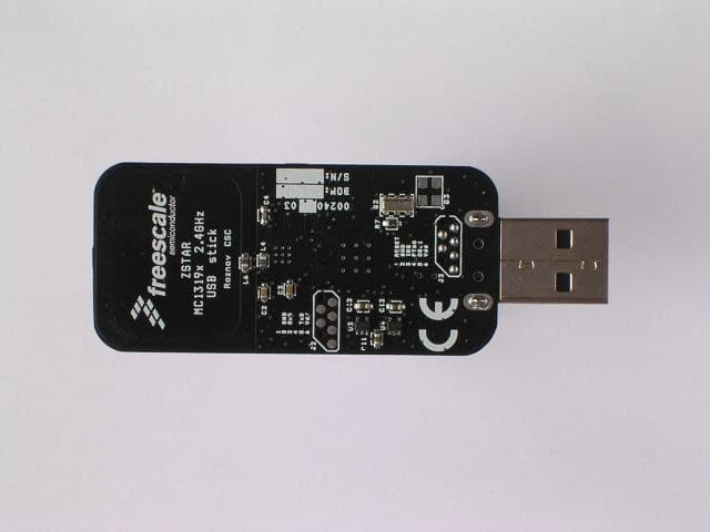
Click to zoom
Application Details
- Equipment Class
- DTS - Digital Transmission System
- Date of Grant
- Nov 02, 2006
- Application Purpose
- Original Equipment
- Date of Application
- Oct 28, 2006
- Equipment Note
- Digital Data ZigBee Device
- Frequency Range
- 2405.00000000 - 2480.00000000
- Country
- United States
Documents & Files
Document Text
Text extracted from the exhibit documents filed with the FCC. Open a document above to read the original.
Users Manual
freescale.com Wireless Sensing Triple Axis Reference design (ZSTAR) Designer Reference Manual ZSTARRM Rev. 0.9 8/2006 Warnings Safety of Radio Frequency Energy The manufacturer has evaluated the transmitter for safe operation for uncontrolled use in the general population. The measured power density at 1 cm is under the threshold established by the FCC and is not required to be tested for specific absorption rate. The manufacturer instructs the user that the transmitter should not be handled or placed near the body continuously for more than 30 minutes while operating. USA: NOTE: This equipment has been tested and found to comply with the limits for a Class B digital device, pursuant to Part 15 of the FCC Rules. These limits are designed to provide reasonable protection against harmful interference in a residential installation. This equipment generates, uses and can radiate radio frequency energy and, if not installed and used in accordance with the instructions, may cause harmful interference to radio communications. However, there is no guarantee that interference will not occur in a particular installation. If this equipment does cause harmful interference to radio or television reception, which can be determined by turning the equipment off and on, the user is encouraged to try to correct the interference by one or more of the following measures: -- Reorient or relocate the receiving antenna. -- Increase the separation between the equipment and receiver. -- Connect the equipment into an outlet on a circuit different from that to which the receiver is connected. -- Consult the dealer or an experienced radio/TV technician for help. This device complies with Part 15 of the FCC Rules. Operation is subject to the following two conditions: (1) this device may not cause harmful interference, and (2) this device must accept any interference received, including interference that may cause undesired operation. Changes or modifications not expressly approved by the party responsible for compliance could void the user's authority to operate the equipment. The antenna(s) used for this transmitter must not be co-located or operating in conjunction with any other antenna or transmitter. Canada: This Class [*] digital apparatus complies with Canadian ICES-003. Cet appareil numériqué de la classe [*] est conformé à la norme NMB-003 du Canada. Europe: TBD Wireless Sensing Triple Axis Reference design, Rev. 0.9 Freescale Semiconductor3 Wireless Sensing Triple Axis Reference design Designer Reference Manual by: Pavel Lajšner and Radomír Kozub Freescale Czech Systems Laboratories Rožnov pod RadhoštČm, Czech Republic To provide the most up-to-date information, the revision of our documents on the World Wide Web will be the most current. Your printed copy may be an earlier revision. To verify you have the latest information available, refer to: http://www.freescale.com The following revision history table summarizes changes contained in this document. For your convenience, the page number designators have been linked to the appropriate location. Revision History Date Revision Level Description Page Number(s) May, 2006 0.02First draftN/A July 2006 0.9Language correction, minor updatesN/A Revision History Wireless Sensing Triple Axis Reference design, Rev. 0.9 4Freescale Semiconductor Wireless Sensing Triple Axis Reference design, Rev. 0.9 Freescale Semiconductor5 Table of Contents Chapter 1 Introduction 1.1Introduction . . . . . . . . . . . . . . . . . . . . . . . . . . . . . . . . . . . . . . . . . . . . . . . . . . . . . . . . . . . . . . . . . 9 1.2MMA7260Q 3-axis Accelerometer Sensor. . . . . . . . . . . . . . . . . . . . . . . . . . . . . . . . . . . . . . . . . . 9 Chapter 2 Wireless Sensing Triple Axis Reference design introduction 2.1Introduction . . . . . . . . . . . . . . . . . . . . . . . . . . . . . . . . . . . . . . . . . . . . . . . . . . . . . . . . . . . . . . . . 11 2.2Featured products . . . . . . . . . . . . . . . . . . . . . . . . . . . . . . . . . . . . . . . . . . . . . . . . . . . . . . . . . . . 12 2.2.1Triple Axis Accelerometer MMA7260Q . . . . . . . . . . . . . . . . . . . . . . . . . . . . . . . . . . . . . . . . 12 2.2.2Microcontroller MC9S08QG8 . . . . . . . . . . . . . . . . . . . . . . . . . . . . . . . . . . . . . . . . . . . . . . . . 12 2.2.3MC13191 2.4 GHz ISM Band Low Power Transceiver . . . . . . . . . . . . . . . . . . . . . . . . . . . . 13 2.2.4Microcontroller MCHC908JW32. . . . . . . . . . . . . . . . . . . . . . . . . . . . . . . . . . . . . . . . . . . . . . 13 Chapter 3 Sensor Board description 3.1Board overview . . . . . . . . . . . . . . . . . . . . . . . . . . . . . . . . . . . . . . . . . . . . . . . . . . . . . . . . . . . . . 15 3.2A/D conversion of XYZ levels . . . . . . . . . . . . . . . . . . . . . . . . . . . . . . . . . . . . . . . . . . . . . . . . . . 17 3.2.1ADC module init: . . . . . . . . . . . . . . . . . . . . . . . . . . . . . . . . . . . . . . . . . . . . . . . . . . . . . . . . . 17 3.2.2ADC measurement. . . . . . . . . . . . . . . . . . . . . . . . . . . . . . . . . . . . . . . . . . . . . . . . . . . . . . . . 18 3.3Power management . . . . . . . . . . . . . . . . . . . . . . . . . . . . . . . . . . . . . . . . . . . . . . . . . . . . . . . . . . 18 3.3.1MC13191 power management features. . . . . . . . . . . . . . . . . . . . . . . . . . . . . . . . . . . . . . . . 20 3.4ZSTAR Sensor Board hardware overview . . . . . . . . . . . . . . . . . . . . . . . . . . . . . . . . . . . . . . . . . 21 3.4.1Analog connections . . . . . . . . . . . . . . . . . . . . . . . . . . . . . . . . . . . . . . . . . . . . . . . . . . . . . . . 21 3.4.2g-select connections . . . . . . . . . . . . . . . . . . . . . . . . . . . . . . . . . . . . . . . . . . . . . . . . . . . . . . 21 3.4.3 BDM (Background Debug Mode) connections. . . . . . . . . . . . . . . . . . . . . . . . . . . . . . . . . . . 21 3.4.4Sensor Board schematics . . . . . . . . . . . . . . . . . . .…
Text truncated - open the document above for the full version.
Users Manual
Wireless Sensing Triple Axis Reference design, Rev. 0.9 33Freescale Semiconductor USB stick board description 4.2.9 USB stick schematics Figure 4-4USB stick schematics 55 44 33 22 11 DCBA TxD RxD PTA0 RxD OSC1 MIRQMRESET MIRQ MRESETMIRQOSC1 PTA0 GND VDD36 GND VDD33 GND GND GND GND GND GND VDD GNDVDD36 GND VDDA GND GND GND VDDGND GND VDD36GND GND VDD33GND VDD36GND GND GND GND VDDVDDVDD GND GNDVDD GND GND GND VDD36GND IRQ VREG33EN VREG33EN IRQ Title Size Design Name: Rev Modify Date: Sheet of Schematic Name:Copyright Freescale POPI Status: Author: 1.1 ZSTAR USB dongle Freescale Semiconductor RCSC1. maje 1009756 61 Roznov p.R., Czech Republic, Europe A4 1 1 Tuesday, August 08, 2006 SCHEMATIC1 General Business Information Radomir Kozub & Pavel Lajsner 2005 X:\ICONN\IC108 - LOW-COST 2.4GHZ AND XYZ ACCELEROME TER DEMO\HW\00240\00240.DSN Title Size Design Name: Rev Modify Date: Sheet of Schematic Name: Copyright Freescale POPI Status: Author: 1.1 ZSTAR USB dongle Freescale Semiconductor RCSC1. maje 1009756 61 Roznov p.R., Czech Republic, Europe A4 1 1 Tuesday, August 08, 2006 SCHEMATIC1 General Business Information Radomir Kozub & Pavel Lajsner 2005 X:\ICONN\IC108 - LOW-COST 2.4GHZ AND XYZ ACCELEROME TER DEMO\HW\00240\00240.DSN Title Size Design Name: Rev Modify Date: Sheet of Schematic Name: Copyright Freescale POPI Status: Author: 1.1 ZSTAR USB dongle Freescale Semiconductor RCSC1. maje 1009756 61 Roznov p.R., Czech Republic, Europe A4 1 1 Tuesday, August 08, 2006 SCHEMATIC1 General Business Information Radomir Kozub & Pavel Lajsner 2005 X:\ICONN\IC108 - LOW-COST 2.4GHZ AND XYZ ACCELEROME TER DEMO\HW\00240\00240.DSN C86.8pFC86.8pF C7 100pF C7 100pF L64.7nHL64.7nH R3 560R3 560 ATTNATTN 1 C1 10nF C1 10nF U4NCP502SQ36T1GU4NCP502SQ36T1G Vin 1 Vout 5 GND 2 Enable 3 SPCLKSPCLK 1 L55.6nHL55.6nH R7 1M R7 1M C131uFC131uF S1 Alps SKRP S1 Alps SKRP 1 34 2 Q2Murata CSTCR6M00G53Q2Murata CSTCR6M00G53 1 2 L322nHL322nH R2 33RR2 33R U2MC68HC908JW32FCU2MC68HC908JW32FC PTA0/KBA0 1 NC 2 NC 3 PTC1/TCLK1 4 PTC3 5 PTB5 6 PTC0/T1CH0 7 PTE7/SS 8 PTE6/MISO 9 PTE5/MOSI 10 PTE4/SPCLK 11 NC 12 PTD0 13 PTD1 14 PTD2 15 PTD3 16 PTD4 17 PTD5 18 PTD6 19 NC 21 PTD7 22 NC 23 NC 24 OSC1 25 OSC2 26 PTB0 27 PTB1 28 VSS33 29 PTE2/PS2CLK/D+ 30 PTE3/D- 31 REG33V 32 VSSPLL 33 CGMXFC 34 VDDPLL 35 PTA7/KBA7 36 RESET 37 IRQ 38 PTA6/KBA6 39 PTA5/KBA5 40 PTC2/T1CH1 41 VDD 42 REG25V 43 VSS 44 PTA4/KBA4 45 PTA3/KBA3 46 PTA2/KBA2 47 PTA1/KBA1 48 NC 20 EPGND 100 EPGND 101 EPGND 102 EPGND 103 EPGND 104 EPGND 105 EPGND 106 EPGND 107 EPGND 108 C4 100pF C4 100pF MOSIMOSI 1 D1LEDD1LED C111uFC111uF C10 2n2 C10 2n2 FB1BEADFB1BEAD 12 J3uMON08J3uMON08 1 2 3 46 5 D3LEDD3LED RTXENRTXEN 1 L422nHL422nH OSC. Q3EPSON-SG310 4.0MHz OSC. Q3EPSON-SG310 4.0MHz 3 24 1 D2LEDD2LED U1MC13191FCU1MC13191FC RFIN- 1 RFIN+ 2 PAO+ 5 PAO- 6 GPIO4 8 GPIO3 9 GPIO2 10 GPIO1 11 RST 12 RXTXEN 13 ATTN 14 CLKO 15 SPICLK 16 MOSI 17 MISO 18 CE 19 IRQ 20 VDDD 21 VDDINT 22 GPIO5 23 GPIO6 24 GPIO7 25 CRYSTAL1 26 CRYSTAL2 27 VDDLO2 28 VDDLO1 29 VDDVCO 30 VBATT 31 VDDA 32 EPGND 36 EPGND 37 EPGND 38 EPGND 39 EPGND 40 EPGND 41 EPGND 35 EPGND 34 EPGND 33 R1 33RR1 33R SSSS 1 J1 USB-A-MALE J1 USB-A-MALE 2134 C310nFC310nF Q1 16MHz NX2520SA Q1 16MHz NX2520SA 1 2 3 4 R5 560R5 560 IRQIRQ 1 R6 1k R6 1k C121uFC121uF FB2BEADFB2BEAD 12 R4 560R4 560 C610nFC610nF C210nFC210nF U3NCP502SQ33T1GU3NCP502SQ33T1G Vin 1 Vout 5 GND 2 Enable 3 J2SerialJ2Serial 1 2 3 46 5 RSTRST 1 C96.8pFC96.8pF MISOMISO 1 C510nFC510nF USB stick board description Wireless Sensing Triple Axis Reference design, Rev. 0.9 34Freescale Semiconductor 4.3 Bill of Materials Table 4-1USB stick bIll of materials ItemQuantityReferencePartManufacturerManufacturer order code 15C1,C2,C3,C5,C610nFTDKC1608CH1E103J 22C4,C7100pFTDKC1608CH1H101J 32C8,C96.8pFTDKC1608CH1H070D 41C102n2TDKC1608CH1H222J 53C11,C12,C131uFTDKC1608JB1C105K 63D1,D2,D3 Kingbright KP-1608SEC KingbrightKP-1608SEC 72FB1,FB2Ferrite beadTDKGLF1608T100M 81J1USB-A-MALEMolex48037-1000 91J2SerialN/A 102L3,L422nHTDKMLG1608B22NJT 111L64.7nHTDKMLG1608B4N7ST 121L55.6nHTDKMLG1608B5N6DT 131Q116MHz NX2520SANDK NX2520SA 16MHz EXS00A-02940 Specification n° EXS10B-07228 141Q2 Murata CSTCR6M00G15 MurataCSTCR6M00G15 152R1,R233R resistor 0603 package 163R3,R4,R5560R resistor 0603 package 171R61k resistor 0603 package 181R71M resistor 0603 package 191U1MC13191FCFreescaleMC13191FC 201U2MCHC908JW32FCFreescaleMCHC908JW32FC 211U3NCP502SQ33T1GON SemiNCP502SQ33T1G 221U4NCP502SQ36T1GON SemiNCP502SQ36T1G 231S1switch SKRPAlps SKRPADE010 (or SKRPACE010 or SKRPABE010) Wireless Sensing Triple Axis Reference design, Rev. 0.9 Freescale Semiconductor35 Chapter 5 Software Design 5.1 Introduction This section describes the design of the ZSTAR software blocks. The software description comprises these topics: • SMAC (Simple Media Access Controller) modifications description •‘Air’ ZSTAR RF protocol protocol description •Serial STAR protocol and ZSTAR extensions (over USB) protocol description •AN2295 Bootloader (over USB) implementation notes 5.2 SMAC (Simple Media Access Controller) The SMAC is a simple ANSI C based code stack available as sample source code which can be used to develop proprietary RF transceiver applications using the MC13191. 5.2.1 SMAC Features •Compact footprint: – 2K FLASH – 10 bytes (+ maximum packet length) RAM – As low as 16kHz bus clock •Can be used to demonstrate coin cell operation for a remote control •MC13191 compatible •Very-low power, proprietary, bi-directional RF communication link •ANSI C source code targeted at the HCS08 core and portable to almost any CPU core (including 4-bit) •Low priority IRQ •Sample application included, extremely easy to use •Liberally commented •Metrowerks CodeWarrior Experimental edition for support 5.2.2 Modifications of SMAC for ZSTAR demo The development of the ZSTAR software is based on the free SMAC stack available from Freescale. The SMAC version used was 4.1a. Two sorts of modifications were made since the original version did not support the HC08 fa…
Text truncated - open the document above for the full version.
Block Diagram
07020-10 Freescale ZStarUSB Block Diagram Page 1 of 1
Cover Letter(s)
07020-10 PTI Reply to ATCB Comments of 101106 Page 1 of 2 1601 FM 1460, Suite B Round Rock, TX 78664 e-mail: [email protected] 512-244-3371 Fax: 512-244-1846 18 October 2006 FCC: RUNZU IC: 6221A-ZU ATCB: Comments 101106 In response to your comments dated 11 Oct 2006 regarding the application for certification of the devices referenced above please find our responses below: 1 Confidentiality has not been requested. Please confirm this is not required. Reply Confirmed. Confidentiality is detrimental to client needs per Comment 10. 2 Give the approval under 15.247, the users manual should state the following or similar: “The antenna(s) used for this transmitter must not be co-located or operating in conjunction with any other antenna or transmitter.” Reply Antenna warning added to user manual, uploaded for review. 3 Users manual should include information for 15.105 and 15.21. Please update. Reply Part 15 Class B standard warning and modification warning added to user manual, uploaded for review. 4 Please justify the test site used for > 1 GHz. It appears an OAT’s was not used. Reply Report incorrectly stated the PTI OATS was used for all emission tests. Test report has been revised to correctly identify the actual test site. The indoor lab area is used for > 1 GHz measurements. Test distance is always 1 meter or less. Path losses for non-incident waves above 1 GHz will exceed 22 dB. The directivity of horn antenna beamwidth is typically 30 degrees for most of the 1 to 18 GHz range. To mitigate effects of the plywood material in the turntable, the EUT is placed above the wooden turntable on a 8 cm thick foam insulator and the horn position adjusted accordingly. This combines for acceptable emission measurement conditions. 5 To measure power, the RBW must be > 6 dB measured bandwidth. It appears that a smaller RBW was used. Please explain/correct as necessary. Reply Agreed, measurement bandwidth was incorrect. New measurements at 3 MHz RBW/VBW taken. Amended test report and other affected documents revised and uploaded for review. 6 It does not appear that values are calculated for the bandedge. Please review. Reply Test report amended accordingly. Includes radiated measurements taken of band edges in the added Adjacent Restricted Band test data. 7 FCC requires compliance to BOTH peak and average limits. Please note that the reading at the 3rd harmonic appears to be over the limits. Limits at 3m are 74 dBuV/m Peak and 54 dBuV/m Average. You can not simply compare average readings to the peak limit. Reply Measurements retaken with peak & average detection and reported amended accordingly. 8 How is this device being handled as a PC peripheral? This device appears to be capable of USB connection to a PC and is therefore also considered a PC peripheral device (in addition to the TX requirements, i.e. Part 15.247, etc.) and is subject to either a Certification or DoC as a PC peripheral. Therefore the application must clarify if you are asking for: a) Certification of the device as a TX, and a DoC has been performed by an appropriately accredited test lab for a PC peripheral b) Certification as a TX + PC peripheral. Note 1: The option b) would be considered as a composite application and 2 certificates (one for the TX, one for the PC peripheral portion) would be issued. Note that there are additional review costs associated with this additional certification. Note 2: To qualify to perform DoC applications, the test lab must be accredited (i.e. NVLAP or A2LA) to perform testing under the DoC procedure. Note 3: Note that for DoC tests, the device is configured with a minimum test configuration as specified by ANSI C63.4 which includes complete computer + 2 I/O devices attached (one may be the EUT) during this particular test. Test photos do not currently support a PC Peripheral device test. Note 4: Each path (DoC or Certification) has particular labeling requirements that must be followed. For DoC authorizations, the label should also include specific DoC labeling information and also the users manual should include information regarding Part 2.1077. If the device is Certified, the FCC ID and current labeling requirements for the TX will cover the labeling requirements. However, additional grants are generated and review costs are higher. Currently labeling and users manual do not appear 07020-10 PTI Reply to ATCB Comments of 101106 Page 2 of 2 to support a DoC. The manufacturer does have a choice of DoC or Certification, however the device labeling and manual information must match the appropriate methods used. Reply Certification is for the transmitter. Peripheral aspect is DoC and laboratory is NVLAP accredited to perform DoC testing. NVLAP Lab Code: 200062-0. Labels & user manual are amended accordingly and uploaded for review. 9 FYI....It is assumed the device is also tested as a PC peripheral under a DoC authorization. Please note that for DoC tests, the device is to be configured with a minimum test configuration as specified by ANSI C63.4 which includes complete computer + 2 I/O devices attached (one may be the EUT) during this particular test. Test photos currently do not cover a correct PC peripheral device configuration, so please ensure testing has been properly performed. Reply Noted. Thank you. 10 FYI...This device appears odd and it is uncertain what it’s purpose will be (development only, etc.). It almost appears modular in nature, but doesn’t meet FCC modular requirements (i.e. modular approval letter, shielding requirements, etc.). Additionally it does not appear to be an end use device since it does not incorporate a case and therefore not available for the general public. Generally something of this nature (a board like design) that is not modular can only approved as a development device. Note that even development devices were not allowed to be Certified until recently as well. Given the explanation given in the operational description, this application will only be reviewed ass…
Text truncated - open the document above for the full version.
Cover Letter(s)
07020-10 PTI Reply to ATCB Comments of 102206 Page 1 of 1 1601 FM 1460, Suite B Round Rock, TX 78664 e-mail: [email protected] 512-244-3371 Fax: 512-244-1846 27 October 2006 FCC: RUNZU IC: 6221A-ZU ATCB: Comments 102206 In response to your comments dated per above please find our responses below: 1) Please note that there appears to be some measurements around 14 and 17 GHz which are reported as peak only, but exceed average limits. Average should be reported as well and shown in compliance with average limits. Reply Freescale Semiconductor revised firmware to reduce transmit power by approximately 6 dB. Spurious and harmonic emissions were measured again. Results available in test report Rev 4. Affected application forms and exposure statements were revised accordingly. 2) There is a reading at 7320 and 7440 which exceeds the limits. Please note that there are 2 limits and the FCC does not recognize a peak-average measurement. One limit is peak, one is average. Correction of a peak measurements for duty factor should be compared to the average limit. Therefore It appears that the peak is in excess of the limits. Please see 15.35 as well. Reply Freescale Semiconductor revised firmware to reduce transmit power by approximately 6 dB. Spurious and harmonic emissions were measured again. Results available in test report Rev 4. Affected application forms and exposure statements were revised accordingly. Eric Lifsey ***
Cover Letter(s)
American Telecommunications Certification Body Inc. 6731 Whittier Ave, McLean, VA 22101 October 29, 2006 RE: Freescale FCC ID: RUNZU After a review of the submitted information, I have a few comments on the above referenced Application. Depending on your responses, kindly understand there may be additional comments. 1) It appears that average measurements are taken and reported. Please note that in pulsed devices, average should only be shown using appropriate duty factor corrections. Given the duty factor correction is > 20 dB in this case, compliance with average limits is shown as long as peak emissions meet peak. Please report appropriately in the future. Timothy R. Johnson Examining Engineer mailto: [email protected] The items indicated above must be submitted before processing can continue on the above referenced application. Failure to provide the requested information may result in application termination. Correspondence should be considered part of the permanent submission and may be viewed from the Internet after a Grant of Equipment Authorization is issued. Please do not respond to this correspondence using the email reply button. In order for your response to be processed expeditiously, you must submit your documents through the AmericanTCB.com website. Also, please note that partial responses increase processing time and should not be submitted. Any questions about the content of this correspondence should be directed to the sender.
Cover Letter(s)
07020-10 Freescale ZStarUSB FCC Authorization Ltr Page 1 of 1
External Photos
07020-10 Freescale ZStarUSB Photos Page 1 of 1 Figure 1 Top Figure 2 Bottom
ID Label/Location Info
07020-10 Freescale ZStarUSB Label Location Page 1 of 1
ID Label/Location Info
07020-10 Freescale ZStarUSB Label Art Rev 2 Page 1 of 1 FCC ID: RUNZU IC: 6744A-ZU (Embedded into silk screen.)
Internal Photos
07020-10 Freescale ZStarUSB Photos Page 1 of 1 Figure 1 Top Figure 2 Bottom
Operational Description
07020-10 Freescale ZStarUSB Operational Description Page 1 of This is one device of a paired transceiver set, one a USB key/stick, the other a battery operated sensor board. The USB stick/key (EUT) connects to a USB port and provides a link to the remote device, a XYZ accelerometer sensor board. This set functions as an engineering demonstration of the Freescale chip set technology and is not intended for final use applications. The EUT is a dual-layer printed circuit board (PCB). It contains the basic design of the MC13191 RF transceiver implementing the ZigBee protocols and is connected through an 8-bit MCHC908JW32 microcontroller to the host device USB port. Its main task is to receive data from the Sensor Board and transfer it to the PC over the USB link. Once inserted into a USB slot, the EUT hunts for the companion Sensor Board by sequentially and slowly polls each channel until a link is made with the companion Sensor Board. Once a link is obtained, data is received in a continuous stream from the Sensor Board. The EUT resumes polling for the Sensor Board if the Sensor Board goes out of range, exhausts its battery, or is manually switched off. ***
RF Exposure Info
07020-10 Freescale ZStarUSB FCC RF Exposure Rev 2 Page 1 of 1 Radio Frequency exposure was evaluated on the EUT to determine compliance with FCC 15.247(b)(5) and RSS-210. The FRIIS transmission formula was applied to the peak power measurements obtained in section 2 of the test report. FCC 1.1307(b) cites the limits for maximum permissible exposure (MPE) from 1.1310 and must be used to evaluate the impact of human exposure to radio frequency energy. The limits from 1.1310 are listed below: Frequency MHz Power Density (mW/cm²) Average Time (Minutes) Limits for Occupational / Controlled Exposures 30-300 1.0 6 300-1500 f/300 6 1500-100,000 5 6 Limits for General Population / Uncontrolled Exposures 30-300 0.2 30 300-1500 f/1500 30 1500-100,000 1.0 30 2 **4 * r GP tyPowerDensi t π = Exposure Frequency (MHz) Calculated EIRP Power (dBm) Linear Power (mW) Distance (cm) Power Density (mW/cm 2 ) Limit (mW/cm 2 ) 2405 -7.57 0.175 1 0.014 1.0 Result: The EUT meets the Maximum Permissible Exposure Limits. SAR Threshold Assessment Frequency (MHz) Power Density (mW/cm 2 ) SAR Threshold mW 2405 0. 014 24.56 Result: The EUT power density is below the SAR threshold. ***
Schematics
TxD RxD PTA0 RxD OSC1 MIRQMRESET MIRQ MRESETMIRQOSC1 PTA0 GND VDD36 GND VDD33 GND GND GND GND GND GND VDD GNDVDD36 GND VDDA GND GND GND VDDGND GND VDD36GND GND VDD33GND VDD36GND GND GND GND VDDVDDVDD GND GNDVDD GND GND GND VDD36GND IRQ VREG33EN VREG33EN IRQ Title Size Design Name: Rev Modify Date :Sheet of Schematic Name:Copyright Freescale POPI Status: Author: 1.0 ZSTAR USB dongle Freescale Semiconductor RCSC1. maje 1009756 61 Roznov p.R., Czech Republic, Europe A4 11 Monday, January 30, 2006 SCHEMATIC1 General Business Information Radomir Kozub & Pavel Lajsner 2005 X:\ICONN\IC108 - LOW-COST 2.4GHZ AND XYZ ACCELEROMETER DEMO\HW\00240\00240.DSN Title Size Design Name: Rev Modify Date :Sheet of Schematic Name:Copyright Freescale POPI Status: Author: 1.0 ZSTAR USB dongle Freescale Semiconductor RCSC1. maje 1009756 61 Roznov p.R., Czech Republic, Europe A4 11 Monday, January 30, 2006 SCHEMATIC1 General Business Information Radomir Kozub & Pavel Lajsner 2005 X:\ICONN\IC108 - LOW-COST 2.4GHZ AND XYZ ACCELEROMETER DEMO\HW\00240\00240.DSN Title Size Design Name: Rev Modify Date :Sheet of Schematic Name:Copyright Freescale POPI Status: Author: 1.0 ZSTAR USB dongle Freescale Semiconductor RCSC1. maje 1009756 61 Roznov p.R., Czech Republic, Europe A4 11 Monday, January 30, 2006 SCHEMATIC1 General Business Information Radomir Kozub & Pavel Lajsner 2005 X:\ICONN\IC108 - LOW-COST 2.4GHZ AND XYZ ACCELEROMETER DEMO\HW\00240\00240.DSN C86.8pFC86.8pF C7 100pF C7 100pF L64.7nHL64.7nH R3 560 R3 560 1 ATTNATTN C1 10nF C1 10nF Vin 1 Vout 5 GND 2 Enable 3 U4NCP502SQ36T1GU4NCP502SQ36T1G 1 SPCLKSPCLK L55.6nHL55.6nH R7 1M R7 1M C131uFC131uF 1 34 2 S1 Alps SKRP S1 Alps SKRP 1 2 Q2Murata CSTCR4M00G53Q2Murata CSTCR4M00G53 L322nHL322nH R2 33RR2 33R PTA0/KBA0 1 NC 2 NC 3 PTC1/TCLK1 4 PTC3 5 PTB5 6 PTC0/T1CH0 7 PTE7/SS 8 PTE6/MISO 9 PTE5/MOSI 10 PTE4/SPCLK 11 NC 12 PTD0 13 PTD1 14 PTD2 15 PTD3 16 PTD4 17 PTD5 18 PTD6 19 NC 21 PTD7 22 NC 23 NC 24 OSC1 25 OSC2 26 PTB0 27 PTB1 28 VSS33 29 PTE2/PS2CLK/D+ 30 PTE3/D- 31 REG33V 32 VSSPLL 33 CGMXFC 34 VDDPLL 35 PTA7/KBA7 36 RESET 37 IRQ 38 PTA6/KBA6 39 PTA5/KBA5 40 PTC2/T1CH1 41 VDD 42 REG25V 43 VSS 44 PTA4/KBA4 45 PTA3/KBA3 46 PTA2/KBA2 47 PTA1/KBA1 48 NC 20 EPGND 100 EPGND 101 EPGND 102 EPGND 103 EPGND 104 EPGND 105 EPGND 106 EPGND 107 EPGND 108 U2MC68HC908JW32FCU2MC68HC908JW32FC C4 100pF C4 100pF 1 MOSIMOSI D1LEDD1LED C111uFC111uF C10 2n2 C10 2n2 12 FB1BEADFB1BEAD 1 2 3 46 5 J3uMON08J3uMON08 D3LEDD3LED 1 RTXENRTXEN L422nHL422nH 3 24 1 OSC. Q3EPSON-SG310 4.0MHz OSC. Q3EPSON-SG310 4.0MHz D2LEDD2LED RFIN- 1 RFIN+ 2 PAO+ 5 PAO- 6 GPIO4 8 GPIO3 9 GPIO2 10 GPIO1 11 RST 12 RXTXEN 13 ATTN 14 CLKO 15 SPICLK 16 MOSI 17 MISO 18 CE 19 IRQ 20 VDDD 21 VDDINT 22 GPIO5 23 GPIO6 24 GPIO7 25 CRYSTAL1 26 CRYSTAL2 27 VDDLO2 28 VDDLO1 29 VDDVCO 30 VBATT 31 VDDA 32 EPGND 36 EPGND 37 EPGND 38 EPGND 39 EPGND 40 EPGND 41 EPGND 35 EPGND 34 EPGND 33 U1MC13191FCU1MC13191FC R1 33RR1 33R 1 SSSS 2134 J1 Molex USB-A-MALE J1 Molex USB-A-MALE C310nFC310nF 1 2 3 4 Q1 16MHz NX2520SA Q1 16MHz NX2520SA R5 560 R5 560 1 IRQIRQ R6 1k R6 1k C121uFC121uF 12 FB2BEADFB2BEAD R4 560 R4 560 C610nFC610nF C210nFC210nF Vin 1 Vout 5 GND 2 Enable 3 U3NCP502SQ33T1GU3NCP502SQ33T1G 1 2 3 46 5 J2SerialJ2Serial 1 RSTRST C96.8pFC96.8pF 1 MISOMISO C510nFC510nF
Test Report
Project 07020-10 Freescale Model ZStar USB Stick Electromagnetic Emission Test Report Prepared for: Freescale Semiconductor 6501 William Cannon Drive West Austin, Texas 78735 By Professional Testing (EMI), Inc. 1601 FM 1460, Suite B Round Rock, Texas 78664 October 27, 2006 Rev 4 Reviewed by Written by Jason Anderson Regulatory Department Manager Eric Lifsey EMC Engineer 07020-10 Rev 4 Page 2 of 36 Table of Contents Title Page ........................................................................................................................................1 Table of Contents ...........................................................................................................................2 Certificate of Compliance..............................................................................................................4 1.0 Introduction........................................................................................................................5 1.1 Scope................................................................................................................................5 1.2 EUT Description ..............................................................................................................5 1.3 EUT Operation.................................................................................................................5 1.4 Test Site ...........................................................................................................................5 1.5 Test Results ......................................................................................................................5 2.0 Power Line Conducted Emissions ....................................................................................6 2.1 Test Procedure .................................................................................................................6 2.2 Test Criteria .....................................................................................................................6 3.0 Peak Output Power............................................................................................................6 3.1 Test Procedure .................................................................................................................6 3.2 Test Criteria .....................................................................................................................7 4.0 Occupied Bandwidth: 6 dB, 20 dB ...................................................................................7 4.1 Test Procedure .................................................................................................................7 4.2 Test Criteria .....................................................................................................................7 5.0 Power Spectral Density......................................................................................................7 5.1 Test Procedure ..........................................…
Text truncated - open the document above for the full version.
Contact Information
Applicant
Robert Fielding(Director, Regulatory and Governmental Affairs)
Technical Contact
Professional Testing (EMI) Inc.Jason Anderson
[email protected]512 244 3371
1601 FM 1460, Ste B · Round Rock, Texas · United States
Non-Technical Contact
Professional Testing (EMI) Inc.Michelle Cantrelle
[email protected]512 244 3371
Test Firm
Professional Testing (EMI), Inc.Michael Royer
Technical Specifications
| # | Rule Parts | Frequency Range | Power Output |
|---|---|---|---|
| 1 | 15C | 2.40 GHz - 2.48 GHz | 180.00 µW |
Other Applications from Freescale Semiconductor, Inc.

RUN-QFM-2202
Apr 20, 2015802.11 b/g/n Wi-Fi module
Equipment Class
DTS - Digital Transmission System
RUNWCT-15W1COILTX
Mar 08, 2015Qi medium power wireless charger
Equipment Class
8CC - Part 18 Consumer Device
RUN-WCT-5WTXMULTI
Dec 29, 2014Wireless Charger Transmitter
Equipment Class
8CC - Part 18 Consumer Device
RUN-USBKW24D
Jul 22, 2014USB Dongle
Equipment Class
DTS - Digital Transmission System
RUN-WCT-5WTXAUTO
May 21, 2014Wireless Charger Transmitter
Equipment Class
8CC - Part 18 Consumer Device