SARHISENSEC389CDMA 2000 Mobile Phone
Hisense Communication Co., Ltd.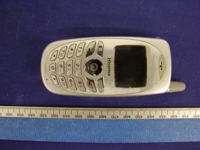
Click to zoom
Application Details
- Equipment Class
- TNE - Licensed Non-Broadcast Transmitter Held to Ear
- Date of Grant
- Jul 18, 2004
- Application Purpose
- Original Equipment
- Date of Application
- Jul 18, 2004
- Equipment Note
- CDMA 2000 Mobile Phone
- Frequency Range
- 824.73000000 - 848.19000000
- Country
- China
Documents & Files
Document Text
Text extracted from the exhibit documents filed with the FCC. Open a document above to read the original.
Users Manual
COMMUNICATIONS C389/C399 CDMA MOBILE PHONE User’s Guide Version: 1.0 Doc ID: C389_UG_V1.0 C389 User’s Guide Welcome to your Phone Headset Jack for Hands-free Headset with MUTE button (sold se parately) Antenna Earpiece Selects a menu item or o ption C or Clear key Erases the last character in text entry, or returns to the previous menu Display Screen OK or Select key Select a menu item o r option End/Power key Switch the phone on or off, end a call, or return you to the home screen Call/Send key Dials a number or answer a call Alphanumeric Keypad Enter numbers, letters, or s ymbols. Navigation key 4-way navigation for scrolling through lists and positioning the cursor. Also accesses shortcuts from the home screen. # key Insert a space durin g text entry * key Switches between uppe r and lower case during text entry Jack for AC ada pter (included). Warning: Inserting an accessory into the incorrect jack willdamage the phone. Performing basic functions To... From the home screen... Switch on the phone Press the End/Power key. Switch off the phone Press and hold the End key for approximately 3 seconds. Make a call Enter the number using the alphanumeric keypad and press the Call/Send key. End a call Press the End/Power key. Answer a call Press the Call/Send key. Verify Own Number Press the OK key to enter the Menu and scroll to Phone Info. Access voicemail Press and hold the 1 and follow the system prompts. Lock the keypad Press and hold the C/Clear key. Unlock the keypad Press 123. Access the All Contacts list Press the RIGHT navigation key. Mute all sounds Press and hold the UP navigation key. Access Recent Calls list Press the LEFT navigation key. Created by RRUAN Page 2 of 2 2004-7-16 C389 User’s Guide Menu Map Main Menu Settings Contacts Recent Calls Silence All Auto Key Guard Supp. Services Sound Display Alerts Call Timers Security Accessories Sys/Network Find View All Business Personal Add New Add to R-UIM Speed Dial List Own Phone Number R-UIM Missed Calls Incoming Calls Outgoing calls Messages Extra Games Inbox Create Message Preformatted Messages Outbox R-UIM Erase Messages Message Settings Stop Watch Alarm Scheduler Calculator Black Jack Video Poker The instructions in this guide assume that your menu appears in Small Icons. To change your menu display so that it appears as Large Icons, see “Menu Format” on page . Navigating the Menus y From the home screen, press the OK key to enter the Menu. y Use the UP and DOWN navigation keys to browse through the menus. y To access soft keys located at the bottom of the display screen, press the DOWN navigation key and use the LEFT and RIGHT navigation keys to select a soft key function. The display texts relating to soft key functions are indicated with a reverse white text in solid background, example, Cancel y Press the OK key to select a menu or menu item. y Press the C key to return to the previous screen. y Press the End key to return to the idle screen. Note: This guide shows you how to select a menu feature as follows: Menu −−> Settings --> Silence All. This example shows that you must select Menu, scroll to and select Settings, then scroll to and select Silence All. Created by RRUAN Page 3 of 3 2004-7-16 C389 User’s Guide Understanding screen icons These icons may appear on the screen of your phone. Icon Function Description Signal Strength Show the signal strength of the network at your current location. The more the bars, the stronger the signal. Network Unavailable Shows that there is no network in service available. Digital Mode Phone is in CDMA digital mode. Roaming Indicates roaming when home network is not available. Keypad Lock Indicates the keypad is locked. In Use Indicates the phone is using the network’s service. MESSAGES You have received one or more text messages. Vibrator Indicates that the ringing tone is muted and vibrator is activated Alarm Alarm or Scheduler has been set. Battery Battery power indicator. More bars indicate a higher power level. D R Created by RRUAN Page 4 of 4 2004-7-16 C389 User’s Guide Contents Getting Started6································································································· Installing your RUIM card and Battery6 ········································································ Charging the battery6 ····························································································· ···············································································Making and Receiving Calls 7 Making a call7 ······································································································ ·································································································· ························································································ ·································································································· ······················································································· ······························································································· ···························································································· ··················································································· ····························································· Answering a call7 Dealing with missed calls7 Calls Forwarding7 Setting up speed dialing 8 Locking the keypad8 Emergency numbers 9 Making calls using a headset9 Entering Letters, Numbers, and Symbols10 Text entry modes10 ································································································ ························································ ····························································································· Switch between Upper and Lower case text input10 Storing Contacts12 Saving a phone number12 ························································································ ··········…
Text truncated - open the document above for the full version.
External Photos
Hisense Communication Co., Ltd. FCC ID: SARHISENSEC389 EXHIBIT C - EUT PHOTOGRAPHS Chassis - Front View Chassis – Rear View Hisense Communication Co., Ltd. FCC ID: SARHISENSEC389 AC Power Adapter
ID Label/Location Info
EXHIBIT A - FCC ID LABELING AND WARNING STATEMENT Proposed FCC ID Label Specifications: Text is black or white in color and is left justified. Labels are silk-screened and shall be “permanently affixed” at a conspicuous location on the EUT. Proposed Label Location on EUT Front View of the EUT/Proposed ID Label Location FCC Warning Statement A FCC Warning Statement is provided in the product manual. FCC ID: SARHISENSEC389
Internal Photos
Hisense Communication Co., Ltd. FCC ID: SARHISENSEC389 EUT – Cover off View EUT – Component View Hisense Communication Co., Ltd. FCC ID: SARHISENSEC389 EUT – Shield Removed View EUT – Solder View
Operational Description
3 Hisense Communication Co., Ltd. ```````````````````````````````````````````````````````````````````````````````````````````` COMMUNICATIONS C389 CDMA MOBILE PHONE Technical Operational Description 4 Hisense Communication Co., Ltd. ```````````````````````````````````````````````````````````````````````````````````````````` Summarize Hisense C399 handset is applied for CDMA 1X network, With Qualcomm MSM6000 chip and ZERO-IF technic C399 has high integrity, high quality of RF and longer idle period .To adopt FLASH ,SRAM chip ,bar shape ,4K colorful and 128X96 pixels LCD ,fixed outer antenna and disassemble battery makes it bright and clear. CDMA2000 1X key technic CDMA2000 1X adopts SRI expend frequency speed and DMSS(direct multi-carrier spread spectrum) (1.2288Mbits/s chip rate in forward and backward channel), so it is smoothly compatible with IS-95(A/B). Because CDMA2000 1X adopt backward correlative demodulation, fast forward power control, transmiting division, Turbo coding technic, its capability is higher than IS-95 and about twice than that of IS-95(A/B) for common voice service under the same condition. 1、Forward fast power control technic CDMA2000 1X adopts Forward fast power control technic. Mobile station will measure Eb/Nt received from traffic channel, compares it with threshold and then transmit indication to base station for adjusting base station transmiting power, the power control speed is up to 800b/s. Due to using Forward rapid power control, the base station transmiting power is lowered, total interfere pulse is decreased, accordingly mobile station signal-to-noise is also decreased and finally the system capability is increased. 2、Forward fast paging channel technic This technic has two usage: 1) Choosing Paging or sleeping state Because base station transmits indecation to mobile station through fast paging channel to decide the mobile station in monitoring paging channel state or low consumption sleeping state, the mobile station need not constantly monitor forward paging channel for a long time, accordingly the mobile station active time is decreased and consumption is saved. 2) Changing configuration Base station transmits recent several minutes system parameter message through forward fast paging channel, makes the mobile station handle these message correspondingly. 3、Forward linking transmitting division technic CDMA2000 1X adopts directly expanding frequency division technic in two way: 1). Orthogonal division method is to separate data stream firstly and then expand frequency for the two data stream with different Orthogonal 5 Hisense Communication Co., Ltd. ```````````````````````````````````````````````````````````````````````````````````````````` Walsh Code and transmit them through two transmiting antenna. 2). Another is air-space expand division This method uses two space separated antenna to transmit interweaved data and the same original Walsh code channel. Using forward link transmiting division technic may decease transmit power, anti Rally fading and increase system capacity. 4、Reverse correlative demodulation Base station uses backward pilot channel to transmit expanding frequency signal to capture the signal of mobile station, and then realizes correlative demodulation with RAKE receiver, improves the backward link capability compared with IS-95 which adoptes no-correlative demodulation, decreased the mobile station transmiting power, increases system capacity. 5.Continued backward air interface waveshape In backward linking, data adopts continued pilot frequency to make data waveshape continued in channel, this method may decrease the interference of outer electromagnetism, improves seaching capability, supports forward power fast control and continued monitor of backward power control 6.Flexible frame length Differing from IS-95, CDMA2000-1X supports multi frame length of 5ms, 10ms, 20ms, 40ms, 80ms and 160ms, different channels support different frame length separately. The forward basic channel ,forward dedicated control channel ,backward basic channel, backward dedicated control channel adoptes 5ms or 20ms fram length, forward supplement channel, backward supplement channel adoptes 20ms、40ms or 80ms frame length,voice channel adoptes 20ms frame length. Short frame may reduce time delay, but demodulation capability is lower. Long frame may lower the demand for transmiting power. Technical description and capability parameter 1.CDMA1X mobile phone accords with following standard YDC 015-2002 《CDMA2000 digital cellular mobile communication network device criterion: mobile station》 YDC 023-2002 《CDMA2000 digital cellular mobile communication network test criterion: mobile station》 YDC 024-2002 《cdma2000 1X mobile station device test criterion:protocol coherence test》 YD 1169.1-2001《the first part of 800MHz CDMA digital cellular mobile communication system electromagnetism compatibility requirement and test method:mobile station and its accessory device》 YD/T965-1998《security requirement and test method of telecom terminal device》 GB/T2434.8-1995 《Electrician and Electron Product Basic Environment Test Regulation Test Ed:Free Falling》 GB 9254-1998《Wireless Interference Limitation and test method of information technic 6 Hisense Communication Co., Ltd. ```````````````````````````````````````````````````````````````````````````````````````````` device》 2.General description: 2.1 Intended Environment Store temperature :-30 to +60°C Working temperature :-20 to +50°C 2.2 Industrial design Size: 101.9x47.1x17.1mm Weight: 72.5g。 2.3 Electronic device speciality (1) Continuum conversation time test condition: according to CDG 35 and charpter 2.1, setting Standard battery: longer than 3.5 hours Continuum idle time test condition: according to CDG 35 and charpter 2.2.2c setting Standard battery: longer than 220 hours Charging time: ≤150 minutes.Battery rating Voltage :3.8V. Standard battery rating volume: 750mAh。 LCD: 4K color and 128 x 96 dot. Key beep …
Text truncated - open the document above for the full version.
Parts List/Tune Up Info
C389 the name of factor y 10 903891001S 1 C389 complete ( argentate ) 2 1 8050100131 903891001S 1 C389 incomplete ( argentate ) 3 2 8020100081 8050100131 1 C389 Main Board 4 3 1140100081 8020100081 A RKAI 7.820.069 1 PCB Board CCTC 3 1140100081 8020100081 B RKAI 7.820.069 1 PCB Board MIT 5 3 1090100061 8050100131 A WM-Y12091-6CLWa 1 LCD module WINTEK 3 1090100061 8050100131 B NLMG-128EB7-CUW1T 1 LCD module LANSER 6 3 10301R1521 8020100081 A MCR10EZHFLR150 1 Resistor ROHM 7 3 1030120221 8020100081 A ERJ2GEF202X 1 Resistor Panasonic 8 3 1030122231 8020100081 A ERJ2GEF222X 3 Resistor Panasonic 9 3 1030151221 8020100081 A ERJ2GEF512X 1 Resistor Panasonic 10 3 1030157211 8020100081 A ERJ2RKF-5761X 3 Resistor Panasonic 11 3 1030110331 8020100081 A ERJ2GEF103X 2 Resistor Panasonic 12 3 1030111311 8020100081 A ERJ2RKF-1132X 2 Resistor Panasonic 13 3 1030118421 8020100081 A ERJ2GEF184X 2 Resistor Panasonic 14 3 1030151411 8020100081 A ERJ2GEF514X 1 Resistor Panasonic 15 3 1030100021 8020100081 A ERJ2GE0R00X 9 Resistor Panasonic 16 3 1030110021 8020100081 A ERJ2GEJ100X 8 Resistor Panasonic 17 3 1030120011 8020100081 A ERJ2GEJ200X 1 Resistor Panasonic 18 3 1030151011 8020100081 A ERJ2GEJ510X 1 Resistor Panasonic 19 3 1030110121 8020100081 A ERJ2GEJ101X 7 Resistor Panasonic 20 3 1030112111 8020100081 A ERJ2GEJ121X 1 Resistor Panasonic 21 3 1030147121 8020100081 A ERJ2GEJ471X 1 Resistor Panasonic 22 3 1030110221 8020100081 A ERJ2GEJ102X 3 Resistor Panasonic 23 3 1030115221 8020100081 A ERJ2GEJ152X 2 Resistor Panasonic 24 3 1030118221 8020100081 A ERJ2GEJ182X 2 Resistor Panasonic 25 3 1030122221 8020100081 A ERJ2GEJ222X 3 Resistor Panasonic 26 3 1030139211 8020100081 A ERJ2GEJ392X 1 Resistor Panasonic modal type amoun t name f BOM LIST NO. class TYPE material type mark 27 3 1030147221 8020100081 A ERJ2GEJ472X 2 Resistor Panasonic 28 3 1030110311 8020100081 A ERJ2GEJ103X 10 Resisto r Panasoni c 29 3 1030118321 8020100081 A ERJ2GEJ183X 1 Resistor Panasonic 30 3 1030120311 8020100081 A ERJ2GEJ203X 1 Resistor Panasonic 31 3 1030122331 8020100081 A ERJ2GEJ223X 1 Resistor Panasonic 32 3 1030147321 8020100081 A ERJ2GEJ473X 1 Resistor Panasonic 33 3 1030110431 8020100081 A ERJ2GEJ104X 2 Resistor Panasonic 34 3 1030447311 8020100081 A NCP18WB473J03RB 1 NTC Thermistor Murata 35 3 1030200011 8020100081 A V0402MHS12NH 10 Varistor Little fuse 36 3 102010R721 8020100081 A CM05CG0R7C50AH 1 MLCC KYOCERA 37 3 102011R021 8020100081 A CM05CG1R0C50AH 1 MLCC KYOCERA 38 3 102012R221 8020100081 A CM05CG2R2C50AH 2 MLCC KYOCERA 39 3 102018R211 8020100081 A CM05CG8R2C50AH 1 MLCC KYOCERA 40 3 1020127031 8020100081 A CM05CG270J50AH 3 MLCC KYOCERA 41 3 1020133031 8020100081 A C1005C0G1H330J 8 MLCC TDK 42 3 1020147031 8020100081 A CM05CG470J50AH 3 MLCC KYOCERA 43 3 1020110131 8020100081 A C1005C0G1H101J 38 MLCC TDK 44 3 1020122131 8020100081 A CM05X7R221K50AH 2 MLCC KYOCERA 45 3 1020110241 8020100081 A CM05X7R102K50AH 9 MLCC KYOCERA 46 3 1020122231 8020100081 A CM05X7R222K50AH 2 MLCC KYOCERA 47 3 1020147221 8020100081 A CM05X7R472K25AH 3 MLCC KYOCERA 48 3 1020110351 8020100081 A CM05X7R103K16AH 7 MLCC KYOCERA 49 3 1020115321 8020100081 A C1005X7R1E153KT 2 MLCC TDK 50 3 1020122351 8020100081 A CM05X7R223K16AT 5 MLCC KYOCERA 51 3 1020168311 8020100081 A CM05X5R683K10AH 1 MLCC KYOCERA 52 3 1020110421 8020100081 A C1005X5R1A104K 40 MLCC TDK 53 3 1020110461 8020100081 A C1005Y5V1C104Z 1 MLCC TDK 54 3 1020147441 8020100081 A CM105Y5V474Z10AT 1 MLCC KYOCERA 55 3 1020168411 8020100081 A C1608X5R0J684K 1 MLCC TDK 56 3 1020110521 8020100081 A C1608X5R1A105K 3 MLCC TDK 57 3 1020122541 8020100081 A C2012X5R1A225K 3 MLCC TDK 58 3 1020147521 8020100081 A C2012Y5V1A475Z 7 MLCC TDK 59 3 1020110641 8020100081 A CM21B106K06AT 1 MLCC KYOCERA 60 3 1020110611 8020100081 A C2012X5R0J106M 1 MLCC TDK 61 3 1020122611 8020100081 A C3225X5R0J226M 2 MLCC TDK 62 3 1020247511 8020100081 A ECST1AZ475R 1 Tantalum chip capacitor Panasonic 3 1020247511 8020100081 B TA-010TCML4R7(M)-P*P-LC* 1 Tantalum chip capacitor FUJITSU 63 3 1020210631 8020100081 A ECST0JZ106R 1 Tantalum chip capacitor Panasonic 3 1020210631 8020100081 B TA-6R3TCML100(M)-P*R-EA K 1 Tantalum chip capacitor FUJITSU 64 3 101012N711 8020100081 A ELJRE2N7DF2 1 chip inductor Panasonic 65 3 101014N711 8020100081 A LL1005-FH4N7S 1 chip inductor TOKYO 3 101014N711 8020100081 B ELJRF4N7DF2 1 chip inductor Panasonic 66 3 1010110N11 8020100081 A LL1005-FH10NJ 3 chip inductor TOKYO 3 1010110N11 8020100081 B ELJRF10NJF2 3 chip inductor Panasonic 67 3 1010122N11 8020100081 A LL1005-FH22NJ 1 chip inductor TOKYO 68 3 1010133N31 8020100081 A ELJRE33NJF2 1 chip inductor Panasonic 69 3 1010147N21 8020100081 A LL1005-FH47NJ 1 chip inductor TOKYO 70 3 1010147N41 8020100081 A LL1608-FS47NJ 1 chip inductor TOKYO 71 3 1010282N11 8020100081 A LL1005-FH82NJ 2 chip inductor TOKYO 72 3 101011N211 8020100081 A LL1608-FS1N2S 1 chip inductor TOKYO 73 3 1040100061 8020100081 A BAS16TT1 2 diode ON Senmiconductor 74 3 1040300011 8020100081 A MIFM3 1 diode xin dianyuan 75 3 1040400011 8020100081 A MAZS3600ML 1 diode Panasonic 76 3 1040300021 8020100081 A MA2S728-(TX) 2 diode Panasonic 77 3 1050100261 8020100081 A DTC124EETL 2 Transistor ROHM 78 3 1050100271 8020100081 A 2SB1424T100Q 1 Transistor ROHM 79 3 1041000041 8020100081 A HSMG- C265 8 LED HP 3 1041000041 8020100081 B PG1111R-TR 8 LED Stanley 80 3 1050100041 8020100081 A 2SA1774TL 1 Transistor ROHM 81 3 1050300021 8020100081 A NTGS3441T1 1 MOSFET ON Senmiconductor 3 1050300021 8020100081 B Si3441BDV 1 MOSFET VISHAY 82 3 1040300071 8020100081 A MA4ZD1400L 1 diode Panasonic 83 3 1060100041 8020100081 A MSM6000 1 CPU QUALCOMM 84 3 1060200031 8020100081 A PM6000 1 power management QUALCOMM 85 3 1060900031 8020100081 A RFL6000 1 Receiver Fronter QUALCOMM 86 3 1060700041 8020100081 A RFR6002 1 Receiver Module QUALCOMM 87 3 1060400021 8020100081 A RFT6102 1 Transmit Module QUALCOMM 88 3 1060300074 8020100081 A K8D3216UTC-TI07 1 FLASH SUMSUNG 3 1060300074 8020100081 B M29DW323DT70Z…
Text truncated - open the document above for the full version.
Parts List/Tune Up Info
Hisense Communication Co., Ltd. ```````````````````````````````````````````````````````````````````````````````````````````` Alignment Procedure and Specification 1. STANDARD TEST CONDITION 1.1 RF input/output Impedance: 50 OHM 1.2 RF cable: 0.7dB<cable loss<1dB, freq: 800MHz~2GHz 1.3 DC power supply: DC 4.8V, within +/-10% ripple 1.4 Radiated shielded test box: cable Loss: 25dB about (900MHz) 1.5 RS232 level shift convert box 1.6 Signal Generator: Output impedance: 50 OHM Output frequency range: 250KHz~3GHz Maximum Output Power: 14dBm 1.7 Signal Analyzer Input impedance: 50 OHM Input frequency range: 9KHz~26.5GHz Maximum input power: within 30dBm 1.8 Base station simulator: Input/Output impedance: 50 OHM RF Input/Output Level Range: -120dBm/1.23MHz to -20dBm/1.23MHz 2. Calibration and Performance Procedure 2.1 Preparative 2.1.1 Power on DUT (device under test), let it run into Factory Test Mode 2.1.2 Conduct DUT to RF calibration system. 2.1.3 Press mouse button and hit “start” menu to start calibration. 2.2 Receiver Calibration: 2.2.1 Digital voltage control amplifier gain offset tuning Limitation:2400~2900 2.2.2 Low noise amplifier gain tuning Limitation: 140~170 2.2.3 Low noise amplifier gain VS different frequency measurement Limitation:-15~+15 2.2.4 Set the AM modulation Signal on the DUT IN/OUT port , then Hisense Communication Co., Ltd. ```````````````````````````````````````````````````````````````````````````````````````````` run IM2(2 step intermediation) calibration. Limitation:0~3 2.3 Transmitter Calibration: 2.3.1 Transmitting power linearity tuning Limitation: Offset 0~10 Slope 0~20 2.3.2 Transmitting power variations over different frequency Limitation:-15~+15 2.3.3 Transmitting high power detecting on reference channel Expect Power LL UL 16.400 130 ~ 170 18.000 140 ~ 180 19.600 150 ~ 190 21.200 160 ~ 210 22.800 170 ~ 230 24.400 180 ~ 250 26.000 190 ~ 255 27.600 200 ~ 255 29.200 220 ~ 255 30.800 220 ~ 255 32.400 220 ~ 255 34.000 220 ~ 255 35.600 220 ~ 255 37.200 220 ~ 255 38.800 220 ~ 255 40.400 220 255 2.3.4 Transmitting high power detecting VS frequency Limitation:-60~40 2.4 RF performance (The minimum standard for high volume production should be compliant with IS-98D spec) 2.4.1 Power on DUT, let it run to network searching mode 2.4.2 Conduct DUT to RF test system. Hisense Communication Co., Ltd. ```````````````````````````````````````````````````````````````````````````````````````````` 2.4.3 Press mouse button and hit “start” menu. Test items are followed: Receiver test: ● Receiver sensitivity and dynamic range ● Demodulation of Forward Traffic Channel in Additive White Gaussian Noise Transmitter Test: ● Frequency accuracy, wave quality, time offset ● Open loop output power range ● Access probe output power ● Open loop output power time response ● Occupied band with ● Maximum RF output power ● Minimum RF output power ● Close loop output power range ● Transmitter conducted spurious emission 2.5 Electrostatic leakage test 2.5.1 Connect DUT with charger and power on DUT 2.5.2 Voltage meter check DUT ’s surface electrostatic voltage within 5 V Limitation: within DC 5V 2.6 Potential current test 2.6.1 Set DC power supply output 3.7V 2.6.2 Connect artificial battery to DUT 2.6.3 In power-off status, check input current with 1mA Limitation: Within 1mA DC 2.7 Radiated sensitivity test 2.7.1 Power on DUT 2.7.2 Put DUT into radiated shielded box connected with base station simulator. 2.7.3 Set up data loop back Minimum standard: -102dBm/1.23MHz,FER 0.5%, confidence 95%. 2.8 Calling test 2.8.1 Connect DUT with base station simulator via RF coupling cable. 2.8.2 Power on DUT 2.8.3 Set up voice loop back Hisense Communication Co., Ltd. ```````````````````````````````````````````````````````````````````````````````````````````` 2.8.4 Check receiver, microphone, buzzer and keypad function. Minimum standard: -75dBm/1.23MHz.
RF Exposure Info
Note: This test report is specially limited to the above client company and the product model only. It may not be duplicated without prior written consent of Bay Area Compliance Laboratory Corporation. This report must not be used by the client to claim product endorsement by NVLAP or any agency of the U.S. Government. SAR EVALUATION REPORT For Hisense Communication Co., Ltd. Hisense Infor. Industrial Park, Economic Technology Dev. District, Qingdao, China, 266510 FCC ID: SARHISENSEC389 This Report Concerns: Original Report Equipment Type: CDMA 2000 Mobile Phone Test Engineer: Daniel Deng / Report No.: R0405263S Report Date: 2004-06-23 Reviewed By: Ling Zhang / Prepared By: Bay Area Compliance Laboratory Corporation 230 Commercial Street Sunnyvale, CA 94085 Tel: (408) 732-9162 Fax: (408) 732 9164 Hisense Communication Co., Ltd. FCC ID: SARHISENSEC389 Report #R0405263S SAR Evaluation Report Page 2 of 60 TABLE OF CONTENTS SUMMARY....................................................................................................................................................................3 1 - REFERENCE ...........................................................................................................................................................4 2 - TESTING EQUIPMENT.........................................................................................................................................5 2.2 EQUIPMENT CALIBRATION CERTIFICATE...............................................................................................................5 3 - EUT DESCRIPTION .............................................................................................................................................17 4 - SYSTEM TEST CONFIGURATION...................................................................................................................18 4.1 JUSTIFICATION.....................................................................................................................................................18 4.2 EUT EXERCISE PROCEDURE................................................................................................................................18 4.3 EQUIPMENT MODIFICATIONS...............................................................................................................................18 5 – CONDUCTED OUTPUT POWER ......................................................................................................................19 5.1 PROVISION APPLICABLE.......................................................................................................................................19 5.2 TEST PROCEDURE................................................................................................................................................19 5.3 TEST EQUIPMENT.................................................................................................................................................19 5.4 TEST RESULTS.....................................................................................................................................................19 6 - DOSIMETRIC ASSESSMENT SETUP...............................................................................................................21 6.1 MEASUREMENT SYSTEM DIAGRAM.....................................................................................................................22 6.2 SYSTEM COMPONENTS.........................................................................................................................................23 6.3 MEASUREMENT UNCERTAINTY............................................................................................................................27 7 - SYSTEM EVALUATION .....................................................................................................................................28 7.1 SIMULATED TISSUE LIQUID PARAMETER CONFIRMATION...................................................................................28 7.2 EVALUATION PROCEDURES..................................................................................................................................28 7.3 SYSTEM ACCURACY VERIFICATION.....................................................................................................................29 SYSTEM VALIDATION RESULT...................................................................................................................................29 7.4 SAR EVALUATION PROCEDURE...........................................................................................................................32 7.5 EXPOSURE LIMITS................................................................................................................................................33 8 - TEST RESULTS ....................................................................................................................................................34 8.1 SAR TEST DATA..................................................................................................................................................34 8.2 PLOTS OF TEST RESULT.......................................................................................................................................34 EXHIBIT A - SAR SETUP PHOTOGRAPHS .........................................................................................................53 BACK SIDE TOUCHING PHANTOM..............................................................................................................................53 FACE TOUCHING PHANTOM.......................................................................................................................................53 LEFT CHEEK TOUCHING PHANTOM............................................................................................................................54 LEFT CHEEK …
Text truncated - open the document above for the full version.
Test Report
Note: The test report is specially limited to the above company and the product model only. It may not be duplicated without prior written consent of Bay Area Compliance Laboratory Corporation. This report must not be used by the client to claim product certification, approval, or endorsement by NVLAP, NIST or any agency of the US Government. FCC PART 22 TYPE APPROVAL EMI MEASUREMENT AND TEST REPORT For Hisense Communication Co., Ltd. Hisense Infor. Industrial Park, Economic Technology Dev. District, Qingdao, China, 266510 FCC ID: SARHISENSEC389 This Report Concerns: Original Report Equipment Type: CDMA 2000 Mobile Phone Test Engineer: Ming Jin Report No.: R0405263 Report Date: 2004-06-22 Reviewed By: Ling Zhang Prepared By: Bay Area Compliance Laboratory Corporation (BACL) 230 Commercial Street Sunnyvale, CA 94085 Tel: (408) 732-9162 Fax: (408) 732 9164 Hisense Communication Co., Ltd. FCC ID: SARHISENSEC389 Report # R0405263Rpt Page 2 of 27 FCC Part 22 Type Approval Report TABLE OF CONTENTS GENERAL INFORMATION.......................................................................................................................................4 PRODUCT DESCRIPTION FOR EQUIPMENT UNDER TEST (EUT) .......................................................................…
Text truncated - open the document above for the full version.
Contact Information
Applicant
Haining Wang
Test Firm
Bay Area Compliance LaboratoryJohn Chan
Technical Specifications
| # | Rule Parts | Frequency Range | Power Output | Emission | Tolerance |
|---|---|---|---|---|---|
| 1 | 22H | 824.73 MHz - 848.19 MHz | 447.00 mW | 1M27F9W | 2.5000000000 ppm |
Other Applications from Hisense Communication Co., Ltd.
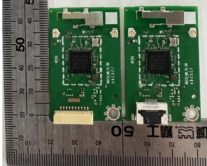
SARMWH411B
Apr 12, 2023WiFi Module
Equipment Class
DTS - Digital Transmission System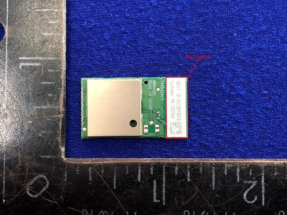
SARMWH409S
Mar 23, 2023MWH409S
Equipment Class
DTS - Digital Transmission System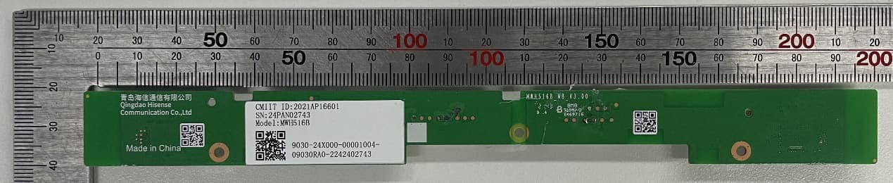
SARMWH516B
Jul 03, 2022BT/Wi-Fi Module
Equipment Class
DSS - Part 15 Spread Spectrum Transmitter
SARMWH519B
Feb 23, 2022Wi-Fi Module
Equipment Class
DTS - Digital Transmission System
SARMW505
Apr 13, 2021BT/Wi-Fi Module
Equipment Class
DSS - Part 15 Spread Spectrum Transmitter