SLYSWXXXXPBNETWORKS SWITCH
Control4 Corporation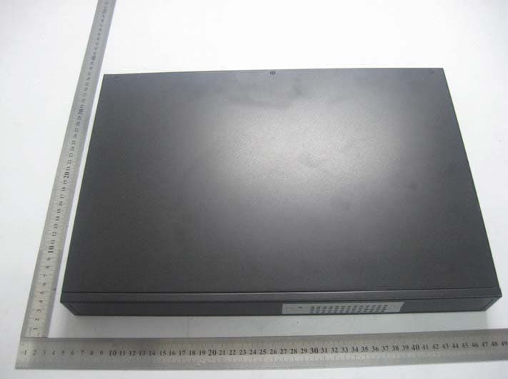
Click to zoom
Application Details
- Equipment Class
- JBP - Part 15 Class B Computing Device Peripheral
- Date of Grant
- Oct 10, 2010
- Application Purpose
- Original Equipment
- Date of Application
- Oct 10, 2010
- Equipment Note
- NETWORKS SWITCH
- Company
- Control4 Corporation
- Country
- United States
Documents & Files
Document Text
Text extracted from the exhibit documents filed with the FCC. Open a document above to read the original.
Users Manual
Web Management User Guide SW24-24PB PoE Switch Web Management User Guide Web Management User Guide Contents Chapter 1、WEB page overview............................................................................................................ 1 1、WEB Access features ................................................................................................................ 1 2、WEB browsing system requirements ........................................................................................ 1 3、WEB browsing session landing ................................................................................................ 1 4、WEB page elements.................................................................................................................. 2 5、The structure of Navigation tree ...............................................................................................3 6、Page button Introduction........................................................................................................... 3 7、Error messages .......................................................................................................................... 3 8、Entry Field ................................................................................................................................ 4 9、Status Field ............................................................................................................................... 4 Chapter 2、WEB page introduction ....................................................................................................... 5 1、Login dialog Box ...................................................................................................................... 5 2、Main Page ................................................................................................................................. 6 3、System Configuration: .............................................................................................................. 6 4、Port Configuration .................................................................................................................. 11 5、MAC binding .......................................................................................................................... 16 6、MAC filtering ......................................................................................................................... 17 7、VLAN Configuration .............................................................................................................. 18 8、SNMP Configuration .............................................................................................................. 20 9、ACL Configuraion .................................................................................................................. 21 10、IP Basic Configuration.......................................................................................................... 22 11、Certification. Authorization. Accounting (AAA) configuration ........................................... 24 11、PoE port configuration .......................................................................................................... 27 Web Management User Guide - 1 - WEB page operating manual This manual focus on describing the WEB page of switch, the user can managed the switch through WEB page. This manual only introduce the simple opetations of the various WEB page of the various switches. This manual includes the following: 1, WEB page overview 2, WEB page description Chapter 1、WEB page overview 1、WEB Access features z Switch provide users with Web access functionality. Via Web browser, users can access switches, manage and configure the switch. WEB accessing‘s main features are: 1, Easy to access: Users can easily access on switch from anywhere using the network. 2, users can visit the WEB pages of the switch by using the familiar Netscape λ Communicator and Microsoft Internet Explorer and other browsers, WEB pages of graphical and tabular format presented to the user. 3, Switch switch provides a wealth of WEB pages, the user can configure and manage vast majority of functions of the switch. 4, WEB page’ function classification &integration, make the user find the relevant pages to configuration and management. 2、WEB browsing system requirements Pls see the form 1。 Form 1: Hardware&Software system requirements CPU Pentium 586 above Memory 128MB above Resolution 800x600 above Color 256 colors above Browser IE4.0 above or Netscape4.01 above Operating system Microsoft® ,Windows95®,Windows98®,WindowsNT®, Windows2000®,WindowsXP®,WindowsME®, WindowsVista®, Linux,Unix ect. Note: Microsoft ®, Windows95 ®, Windows98 ®, WindowsNT ®, Windows2000 ®, WindowsXP ®, Windows ME ®, WindowsVista ® is a registered trademark of Microsoft Corp. All other product names, trademarks, registered trademarks and service marks, copyrights held by their respective owners. 3、WEB browsing session landing z Before start Web browsing session ,the user need to make sure: 1. has configure the IP of switch, under the default case, the switch VLAN1 interface IP address is 192.168.0.1, 2. subnet mask is 255.255.255.0. 3. has a Web browser installed on the host to connect to the network, and the host Web Management User Guide - 2 - can PING-pass switches. 4. After completing these two tasks, the user put the right address on the browser's address bar of the switch and press Enter to enter the switch after the Web login page, shown in Figure 1. When the multi-user management is not enabled, the user login need for anonymous Web user (admin) password for authentication, and only entered the correct password can access Web, anonymous user password by default is empty. If the system enabled a multi-user management and configure the privileged user, the anonymous user's password will not force users to visit the Web.user access not do anonymous user's password authentication, bu…
Text truncated - open the document above for the full version.
External Photos
Pakedge Device and Software Inc. Model: SW24-24PB REPORT NO.: STR10088080I FCC PART 15B EXHIBIT 2 - EUT EXTERNAL PHOTOGRAPHS EUT View 1 EUT View 2
ID Label/Location Info
Pakedge Device and Software Inc. Model: SW24-24PB REPORT NO.: STR10088080I FCC PART 15B EXHIBIT 1- PRODUCT LABELING Proposed FCC ID Label Format FCC ID: SLYSWXXXXPB This device complies with Part 15 of the FCC Rules. Operation is subject to the following two conditions: (1) This device may not cause harmful interference, and (2) This device must accept any interference received, including interference that may cause undesired operation. Specifications : Text is Black in color and justified. Labels are printed in indelible ink on permanent adhesive silk-screened onto the EUT or shall be affixed at a conspicuous location on the EUT. Proposed Label Location on EUT FCC ID Label Location
ID Label/Location Info
Pakedge Device and Software Inc. Model: SW24-24PB REPORT NO.: STR10088080I FCC PART 15B EXHIBIT 1- PRODUCT LABELING Proposed FCC ID Label Format FCC ID: SLYSWXXXXPB This device complies with Part 15 of the FCC Rules. Operation is subject to the following two conditions: (1) This device may not cause harmful interference, and (2) This device must accept any interference received, including interference that may cause undesired operation. Specifications : Text is Black in color and justified. Labels are printed in indelible ink on permanent adhesive silk-screened onto the EUT or shall be affixed at a conspicuous location on the EUT. Proposed Label Location on EUT FCC ID Label Location
Internal Photos
Pakedge Device and Software Inc. Model: SW24-24PB REPORT NO.: STR10088080I FCC PART 15B EXHIBIT 3 - EUT INTERNAL PHOTOGRAPHS EUT Housing and Board View Solder Board-Component View 1 Pakedge Device and Software Inc. Model: SW24-24PB REPORT NO.: STR10088080I FCC PART 15B Solder Board-Component View 2 Solder Board-Component View 3 Pakedge Device and Software Inc. Model: SW24-24PB REPORT NO.: STR10088080I FCC PART 15B Solder Board-Component View 4 Solder Board-Component View 5 Pakedge Device and Software Inc. Model: SW24-24PB REPORT NO.: STR10088080I FCC PART 15B Solder Board-Component View 6 Solder Board-Component View 7 Pakedge Device and Software Inc. Model: SW24-24PB REPORT NO.: STR10088080I FCC PART 15B Solder Board-Component View 8 Solder Board-Component View 9 Pakedge Device and Software Inc. Model: SW24-24PB REPORT NO.: STR10088080I FCC PART 15B Solder Board-Component View 10 Solder Board-Component View 11 Pakedge Device and Software Inc. Model: SW24-24PB REPORT NO.: STR10088080I FCC PART 15B Solder Board-Component View 12
Operational Description
Circuit Description The product is a fast ethernet switch with maximum 100Mbps transmission rate,the IC-BCM53242 is a master control unit with a 50 MHz oscillator as base clock frequency, and the master function as follows: 1. To processing the communication data for uplink and downlink 2. Link to computer network terminal via port 1~24 RJ45, 3. The power supply is AC110~240V/50~60Hz
Schematics
55 44 33 22 11 D D C C B B A A DC-to-DC Magnetic BCM53242 BCM5221PHYAD=06h SDRAM8Mbitx16(16MB) 50MHz Xtal 25MHzXtal MII 2.5V RJ45 Magnetic RS232DB-9 SFP Magnetic RJ45+X'mr Magnetic RvMII 3.3V RJ45 2X4 BCM5482S Copper/Fiber Auto-Detect 5V [For WSS, SDRAM range 2x4Mx16~2x8Mx16] SDRAM8Mbitx16(16MB) SFP RJ45 2X4 RJ45 2X4 Magnetic EEPROM Flash4Mbit x16(8MB) SPI 2.5V Center Tap RGMII MDC/MDIO MII 25MHzXtal 48MHzXtal TF-331 DC-to-DC RJ45 BCM5836 optional for Management RGMII 1.22V1.2V1.25V BCM5324 24+2G Managed Switch 2.0 Block Diagram B 110 Monday, June 21, 2010 TitleSize Document Number Rev Date: Sheet of 55 44 33 22 11 D D C C B B A A 定位螺孔 VCC_2.5/3A +5V TO +2.5V +5V TO +3.3V Additional 1.22V output FOR BCM5482 1.25V power supply for BCM5836 Output is 1.25V Output is 1.22V MAIN POWER 5V/0.1A FAN5V/0.1A FAN 光学定位点 BCM5324 24+2G Managed Switch 2.0 DC-DC C 210 Monday, June 21, 2010 TitleSize Document Number Rev Date: Sheet of +2.5V +3.3V +5V +2.5V +5V +3.3V +5V +5V +1.22V +2.5V +1.25V +3.3V +2.5V +3.3V +5V Q1A NTD60N02R 1 32 G SD R6 10K 1% C34 0.01uF M9 INSTALL_HOLE C68 0.1uF EC18 47UF/16V 12 C2310nF EC4 470UF/16V 12 L2 BEAD H3 C63 0.1uF + EC8 1000uF/16V 12 EC12 4.7uF R112.2K 1% C270.1uF L610uH 5A DIP C3 0.22UF/0805 J1 CONN_6P_PWR 123456 VDD_INVDD_INVDD_IN GND_INGND_INGND_IN EC9 47UF/16V 12 C250.1uF C490.1uF M7 INSTALL_HOLE C48 0.1uF Q2A NTD60N02R 1 32 G SD C223 0.1uF R5 12.4K 1% C22 470pF C37 0.01uF EC16 47UF/16V 12 R4 10/1206 C110.1uF C59 0.1uF EC11 47UF/16V 12 C17 0.1uF EC2 470UF/16V 12 C54 0.1uF C390.01uF C18 0.1uF U1 AMS1084 1 2 3 4 ADJ OUTPUT INPUT OUTPUT L3 100 100MHz 3A R7 11.8K 1% C31 0.1uF C7 0.1uF C44 0.1uF + C10 47uF/16V C19 4.7U/0805 C40 0.1uF C222 0.1uF AT9173 U2 786 4321 5 9 VCNTLVCNTLVCNTL VoutREFGNDVin VCNTL GND C9 4.7U/0805 C13 0.1uF L4 100 100MHz 3A C52 0.1uF C30 4.7U/0805 EC3 470UF/16V 12 C46 0.1uF D1BAT54W 12 3 L7 120@100MHz L1 100 100MHz 3A C20 4.7U/0805 C6 4.7U/0805 C41 0.1uF C55 0.1uF C60 0.1uF R131.05K 1% C64 0.1uF C14 0.01uF M11 INSTALL_HOLE M1 INSTALL_HOLE C1 0.1uF C154.7U/0805 C32 0.01uF C36 0.01uF C380.1uF AT9173 U4 786 4321 5 9 VCNTLVCNTLVCNTL VoutREFGNDVin VCNTL GND C45 0.1uF C42 0.1uF L5 100 100MHz 3A C50 0.1uF C28 4.7U/0805 EC15 47UF/16V 12 EC13 47UF/16V 12 C224 0.1uF EC17 47UF/16V 12 EC14 10uF/16V C47 0.1uF R9 4.7 1% C58 0.1uF + EC7 1000uF/16V 12 C8 0.01uF C4 0.01uF C29 0.01uF C43 0.1uF C225 0.1uF R14 12.4K 1% C67 0.1uF C12 1U/0805 C21 1U/0805 C35 0.01uF C530.1uF M8 INSTALL_HOLE EC1 470UF/16V 12 EC10 47UF/16V 12 C2 0.01uF EC5 470UF/16V 12 R8 4.7 1% C57 0.1uF H1 R15 12.4K 1% R2 200 1% R1 120 1% H2 FAN1FAN(2PIN) 21 EC6 47UF/16V 12 C26 0.01uF R102.2 1% EC19 47UF/16V 12 U3 ISL6520ACB 12 3 4 567 8 BOOT UGATE GND LGATE VCCFBCOMP PHASE C33 0.01uF M6 INSTALL_HOLE M4 INSTALL_HOLE R330.1K 1% L8 120@100MHz R12 100 1% FAN2FAN(2PIN) 21 C56 0.1uF L1810uH 5A SMD_NC C16 4.7U/0805 + C547uF/16V C24 1000pF M10 INSTALL_HOLE H4 M2 INSTALL_HOLE 55 44 33 22 11 D D C C B B A A Close to BCM5324 Close to BCM5324 TO CPU BCM5324 24+2G Managed Switch 2.0 5324 Integrated PHY, RGMII C 310 Monday, June 21, 2010 TitleSize Document Number Rev Date: Sheet of TDN_11TDP_11RDN_11RDP_11TDN_10TDP_10RDN_10RDP_10TDN_9TDP_9RDN_9RDP_9TDN_8TDP_8RDN_8RDP_8TDN_7TDP_7RDN_7RDP_7TDN_6TDP_6RDN_6RDP_6 TDN_5TDP_5RDN_5RDP_5TDN_4TDP_4RDN_4RDP_4TDN_3TDP_3RDN_3RDP_3TDN_2TDP_2RDN_2RDP_2TDN_1TDP_1RDN_1RDP_1TDN_0TDP_0RDN_0RDP_0 TDN_12TDP_12RDP_12RDN_12TDP_13TDN_13RDN_13RDP_13RDP_15TDP_14TDN_15TDN_14RDN_14RDP_14TDP_15RDN_15RDP_17RDP_18RDN_18RDP_19TDP_16TDN_17TDN_18TDN_19TDN_16RDN_16RDP_16TDP_19RDN_19TDP_17RDN_17TDP_18RDP_21RDP_22RDN_22RDP_23TDP_20TDN_21TDN_22TDN_23TDN_20RDN_20RDP_20TDP_23RDN_23TDP_21RDN_21TDP_22 M_CRS M_COL M_RXCLKM_TXCLKM_TXD0M_TXD1M_TXD2M_TXD3M_TXEN M_TXD1 M_RXCLKM_RXDVMOSI MISOM_RXD2M_TXD3 SS M_RXD0 M_TXD2 M_TXCLKSCKM_TXEN M_RXD3M_TXD0M_RXD1MDC MDIO CPU_LED RESET_SOFT RESET_CPU GPIO2 GPIO3 GPIO4 GPIO5 GMII0_TXD0 6 GMII0_TXD1 6 GMII0_TXD2 6 GMII0_TXD3 6 GMII0_RXD0 6 GMII0_RXD1 6 GMII0_RXD2 6 GMII0_RXD3 6 GMII0_GTX_CLK 6 GMII0_TX_EN 6 GMII0_RX_CLK 6 GMII0_RX_DV 6 GMII1_TXD0 6 GMII1_TXD1 6 GMII1_TXD2 6 GMII1_TXD3 6 GMII1_RXD0 6 GMII1_RXD1 6 GMII1_RXD2 6 GMII1_RXD3 6 GMII1_GTX_CLK 6 GMII1_TX_EN 6 GMII1_RX_CLK 6 GMII1_RX_DV 6 RDP_0 5 RDP_1 5 RDP_2 5 RDP_3 5 RDP_4 5 RDP_5 5 RDP_6 5RDP_7 5RDP_8 5RDP_9 5RDP_10 5RDP_11 5 RDN_0 5 RDN_1 5 RDN_2 5 RDN_3 5 RDN_4 5 RDN_5 5 RDN_6 5RDN_7 5RDN_8 5RDN_9 5RDN_10 5RDN_11 5 TDP_0 5 TDP_1 5 TDP_2 5 TDP_3 5 TDP_4 5 TDP_5 5 TDP_6 5 TDP_7 5 TDP_8 5 TDP_9 5 TDP_10 5TDP_11 5 TDN_0 5 TDN_1 5 TDN_2 5 TDN_3 5 TDN_4 5 TDN_5 5 TDN_6 5TDN_7 5TDN_8 5TDN_9 5TDN_10 5TDN_11 5 TDN_12 5TDN_13 5TDN_14 5TDN_15 5TDN_16 5TDN_17 5TDN_18 5TDN_19 5TDN_20 5TDN_21 5TDN_22 5TDN_23 5TDP_12 5TDP_13 5TDP_14 5TDP_15 5TDP_16 5TDP_17 5TDP_18 5TDP_19 5TDP_20 5TDP_21 5TDP_22 5TDP_23 5RDN_12 5RDN_13 5RDN_14 5RDN_15 5RDN_16 5RDN_17 5RDN_18 5RDN_19 5RDN_20 5RDN_21 5RDN_22 5RDN_23 5RDP_12 5RDP_13 5RDP_14 5RDP_15 5RDP_16 5RDP_17 5RDP_18 5RDP_19 5RDP_20 5RDP_21 5RDP_22 5RDP_23 5 MDC 4,6,8 MDIO 4,6,8 M_TXD0 8M_TXD1 8M_TXD2 8M_TXD3 8M_TXEN 8M_RXCLK 8M_TXCLK 8M_RXDV 8M_RXD0 8M_RXD1 8M_RXD2 8M_RXD3 8 RESET_CPU 8,9 RESET_SOFT 8,9 GPIO2 8 GPIO4 8 GPIO3 8 GPIO5 8 RXD 7 TXD 7 MISO 4,8 SCK 4,8 MOSI 4,8SS 4,8 CPU_LED 4,8 +2.5V +2.5V +2.5V+3.3V +3.3V R25 4.7K R17 1K(NC) R29 22 R40 22 J10HEADER 5*2-2.54mm 13579 2468 10 13579 246810 R20 22 R32 22 R36 22 R26 4.7K(NC) R33 22 R27 0 R39 22 R19 22 R38 22 R24 0 R28 0 R18 22 R35 22 R30 22 R34 22 GMII0 Interface (port 25)GMII1 Interface (port 26) MII Interface ( port 24) Media Interface (po rt [0:11]) Media Interface (port [12:23]) MDIO Inte rface U5A BCM5324 W19W18Y19Y20U16U17V18V17W17W16Y17Y18U14U15V16V15 Y16 Y15 W14 W15 U12 U13 V14 V13 Y14 Y13 W12 W13 U10 U11 V12 V11 C19 B19A19 C18 B18A18 C17 B17E19E20 F18F19 G18 F17 G17 H17C20 A20 D20 E18B20 D16 E17 J17 K17 D18D19C12 B12A12 C11 B11A11 C10 B10A14B14 C14 A15B15 C15 A16B16A13 D11 B13 D15D12D10D14C16 A17 Y1 Y2 W3 W2 U5 U4 V3 V4 Y3 Y4 W5 W4 U7 U6 V5 V6 Y5 Y6 W7 W6 U9 U8 V7 V8 Y7 Y8 W9 W8 V10 V9 Y9 Y10 A5 C6 B6 A6 A7 B7 C7 D7 A8 B8 B9 A…
Text truncated - open the document above for the full version.
Test Report
Pakedge Device and Software Inc. Model: SW24-24PB REPORT NO.: STR10088080I PAGE 1 OF 13 FCC PART 15B FCC PART 15B MEASUREMENT AND TEST REPORT FOR Pakedge Device and Software Inc. 1163 Triton Drive Foster City, CA 94404 FCC ID: SLYSWXXXXPB Report Concerns: Original Report Equipment Type: NETWORKS SWITCH Model: SW24-24PB Report No.: STR10088080I Test Date: 2010-08-13 to 2010-08-20 Issue Date: 2010-10-11 Tested By: Jason Chen / Engineer Reviewed By: Lahm Peng / EMC Manager Approved & Authorized By: Jandy so/PSQ Manager Prepared By: SEM.Test Compliance Service Co., Ltd 3/F, Jinbao Commerce Building, Xin'an Fanshen Road, Bao'an District, Shenzhen, P.R.C.(518101) Tel.: +86-755-33663308 Fax.: +86-755-33663309 Website: www.semtest.com.cn Note: This test report is limited to the above client company and the product model only. It may not be duplicated without prior permitted by SEM.Test Compliance Service Co., Ltd . Pakedge Device and Software Inc. Model: SW24-24PB REPORT NO.: STR10088080I PAGE 2 OF 13 FCC PART 15B TABLE OF CONTENTS 1. GENERAL INFORMATION ...................................................................................................................................3 1.1 PRODUCT DESCRIPTION FOR EQUIPMENT UNDER TEST (EUT)...............................................................................3 1.2 TEST STANDARDS...................................................................................................................................................3 1.3 RELATED SUBMITTAL(S)/GRANT(S) .......................................................................................................................3 1.4 TEST METHODOLOGY.............................................................................................................................................3 1.5 TEST FACILITY.......................................................................................................................................................4 1.6 EUT EXERCISE SOFTWARE....................................................................................................................................4 1.7 ACCESSORIES EQUIPMENT LIST AND DETAILS.......................................................................................................4 1.8 EUT CABLE LIST AND DETAILS.............................................................................................................................4 2. SUMMARY OF TEST RESULTS ...........................................................................................................................5 3. §15.107 (A)- CONDUCTED EMISSION .................................................................................................................6 3.1 MEASUREMENT UNCERTAINTY..............................................................................................................................6 3.2 TEST EQUIPMENT LIST AND DETAILS.....................................................................................................................6 3.3 TEST PROCEDURE...................................................................................................................................................6 3.4 BASIC TEST SETUP BLOCK DIAGRAM.....................................................................................................................6 3.5 ENVIRONMENTAL CONDITIONS..............................................................................................................................7 3.6 TEST RECEIVER SETUP...........................................................................................................................................7 3.7 SUMMARY OF TEST RESULTS/PLOTS......................................................................................................................7 3.8 CONDUCTED EMISSIONS TEST DATA......................................................................................................................7 4. §15.109(A)- RADIATED EMISSION ....................................................................................................................10 4.1 MEASUREMENT UNCERTAINTY............................................................................................................................10 4.2 TEST EQUIPMENT LIST AND DETAILS...................................................................................................................10 4.3 TEST PROCEDURE.................................................................................................................................................10 4.4 TEST RECEIVER SETUP.........................................................................................................................................11 4.5 CORRECTED AMPLITUDE & MARGIN CALCULATION............................................................................................11 4.6 ENVIRONMENTAL CONDITIONS............................................................................................................................11 4.7 SUMMARY OF TEST RESULTS/PLOTS....................................................................................................................11 Pakedge Device and Software Inc. Model: SW24-24PB REPORT NO.: STR10088080I PAGE 3 OF 13 FCC PART 15B 1. GENERAL INFORMATION 1.1 Product Description for Equipment Under Test (EUT) Client Information Applicant: Pakedge Device and Software Inc. Address of applicant: 1163 Triton Drive Foster City, CA 94494 Manufacturer: Quickte Technology Co., Ltd. Address of manufacturer: 2nd/F, 8 Block, Xinwu Industrial Area, Xili, Nanshan District, Shenzhen, Guangdong, PRC General Description of E.U.T Items Description EUT Description: NETWORKS SWITCH Trade Name: Dakedge Model No.: SW24-24PB Add Models: SW16-16PB, SW8-8PB, QTS20 Rated Voltage: AC 110-240V Rated Current: 4A Size: 42.5x29.0 x4.4 cm For more information refer to the circuit diagram form and the user’s ma…
Text truncated - open the document above for the full version.
Test Setup Photos
Pakedge Device and Software Inc. Model: SW24-24PB REPORT NO.: STR10088080I FCC PART 15B EXHIBIT 4 - TEST SETUP PHOTOGRAPHS Conduction Emission Test View Radiation Emission Test View
Contact Information
Applicant
Roger Midgley(Sr. Regulatory Compliance Engineer)
Test Firm
SEM.Test Compliance Service Co., Ltd.Jandy So
Technical Specifications
| # | Rule Parts | Frequency Range | Power Output |
|---|---|---|---|
| 1 | 15B | - | - |
Other Applications from Control4 Corporation

SLY-WK1X22
Apr 13, 2015802.11ac Dual Band Access Point
Equipment Class
NII - Unlicensed National Information Infrastructure TX
SLY-WAPC11G
Oct 27, 2004Carrier Grade Embeddable Access Point
Equipment Class
DTS - Digital Transmission System