SWUDE-PCA20Portable Card Checking Machine (RFID)
Duali Inc.
Click to zoom
Application Details
- Equipment Class
- DXT - Part 15 Low Power Transceiver, Rx Verified
- Date of Grant
- Oct 14, 2007
- Application Purpose
- Original Equipment
- Date of Application
- Oct 14, 2007
- Equipment Note
- Portable Card Checking Machine (RFID)
- Frequency Range
- 13.56000000 - 13.56000000
- Company
- Duali Inc.
- Country
- South Korea
Documents & Files
Document Text
Text extracted from the exhibit documents filed with the FCC. Open a document above to read the original.
Users Manual
BEIJING LINE 10 AUTOMATIC FARE COLLECTION PROJECT User Guide for PTCM(Portable Card Checking Machine) ( Model Name : SA-74PS01, SA-74PB01, SA-74PC01) REVISION NUMBER: 1.00 27 February, 2007 SAMSUNG SDS Copyright ⓒ 2006 Samsung SDS Co., Ltd. All rights reserved. You are strictly prohibited to copy, disclose, distribute, or use this document in part or as a whole for any purposes other than those for which this document is disclosed. This document is copyrighted and contains confidential information and other intellectual property rights of Samsung SDS Co., Ltd. Any unauthorized use, copy, disclosure or distribution constitutes infringement of Samsung SDS’ intellectual property rights. 1. Outline This Device is portable smart card reader and you can use this Device as electronic cash or token Marker, Device for purchase, Device for load according to service provider. And this one is communicated with PC or other upper device using USB. There are 4 SAM in this device, so this one can support several kinds of electronic payment system. And It is easy to make program for service provider, because this device use WINDOWS CE for OS. Basic data in this device is as following. Item Specification note CPU ARM9, S3C2410 32bit RISC SIZE 215mm(w) x 86mm(l) x 37mm(h) Weight Under 300g Not include Battery Battery Capacity 3.7V / 2200mAh Over 4 hours to use Program memory1 32MBYTE NAND FLASH WIN-CE part Program memory2 32MBYTE NAND FLASH USER APP, DATA part Data memory 64MBYTE SDRAM Execute program HOST Communication USB1.1, RS-232 Basic RF Card that can be used ISO 14443 A/B, Mifare Contact Card that can be used ISO 7816 T=0 Security Module 4 SIM SOCKET Electronic Specification of Battery charger Over DC12V, 700mA Adapter 1 2. Configuration 2 2.1 Device Configuration - Portable Card Checker (Main PCB, Contact Card/ RF Card/ SAM Control PCB, Keypad PCB, LCD) - Battery Charger - Battery 2 EA - Adapter - Communication cable 2.2 System configuration Diagram 3 Upper part Device USB Communication CABLE CRADLE (Battery Charger) 2.3 Main board Block Diagram And Explanation Figure 2-1 figure 4 CAD (Card Acceptance Device) ISO 14443A/B, Mifare Antenna MAIN CPU ARM920T Core 32bit RISC Processor RTC 내장 RS232 Flash Memory 32MB (B/L 200000) SIM SLOT x4 for SAM BUZZER DC/DC CONVERTER KEYPAD 19Keys(0~9#,F1,F2,F3,F4 ,PWR,ENT,CLR) AC/DC Adaptor Color TFT LCD LED BACKLIGHT USBI/FtoSC Flash Memory 32MB (WIN-CE) Boot ROM SDRAM Memory 64MB Battery 3.7V /2200mAh - MAIN CPU: Main CPU is Samsung ARM9 Core S3C2410. And this CPU is 32bit RISC CPU. This CPU has RTC, 2 UART, USB. - CAD(Card Acceptance Device): The part for reading Contact Card, 4 SAM and Contact less Card. - Contactless Smart Card Standard: ISO14443 Type A, Type B, Mifare - Card communication Speed: 106Kbps - Range for reading: 50mm(Card), 30mm(Token) - Contact Smart Card Standard: ISO7816, T=0 - Contact Smart Card Slot: User Card(1), SIM Type(4) - LCD : 960 x 240 Color TFT LCD(LED Backlight) Parameter Specification Screen Size 2.5 Inch Display Format 960 * 240 Active Area 50.4mm(W) * 37.8mm(H) Dot Pitch 0.525mm(W) * 0.1575mm(H) Pixel Configuration R.G.B Delta Outline Dimension 60.73mm(W) * 47.07mm(H) * 2.54mm(T) Weight 12g Operation Temperature 0 ~ 60 °C Storage Temperature -25 ~ 80 °C - Buzzer: Control Frequency using Buzzer connected with Timer Output Por. - DC/DC Converter: All part that create 5V, 3.3V, 2.0V power for executing using Battery power. 5 - Keypad: There are 19 button such as 0~9,#,*,F1,F2,F3,F4,Power,Enter,Clear. - SIM Slot: There are 4 SAM Slot in Main board and CAD part control this SAM slot. - Data memory: 64MBytes SDRAM - B/L Memory: 32MBytes NAND Flash - Program memory: 32MBytes NAND Flash - Boot ROM: 64Kbytes Flash - RS-232: Communication port for Debug - USB: USB is used as communication part when Device is connected with upper Device using USB. - RTC Battery: RTC is on CPU. And when power is off, RTC is running using other battery. - Battery: Lithium ion or Lithium polymer, 3.7V/2200mAh - Minimum waiting time is 6 hours. - Enable to detach and to check card over 1500 times. - Under voltage notification - CRADDLE: Charger Module - Input power: Adapter power (DC 12V) - Lithium ion(or Lithium polymer) For Battery charger. - Charging time: Under 4 hours - Over charge protection - Detect decrease rate of power. - The number of charging and discharge: Over 500 times. - Battery weight: 66g - Adapter: Over Power 12V, 700mA. - Mast cell burst Factor(MCBF): Over 100,000 times - Mean Time to Repair(MTTR) : Under 10 minutes and easy to maintenance. 6 3. External Specification 3.1 Device Visual Diagram Figure 3-1 figure Battery USB USB & Power 3.2 External Size - 215mm(w) x 86mm(l) x 37mm(h) 3.3 Weight - Under 300g(Not include Battery) 7 960*240 LCD Display Card hole Contact/Contactless IC Card Reading Part(Antenna) Battery Charger Button 4. Electronic Specification 4.1 Power Specification - Input Power: AC 220V / 50Hz - Adapter output power: DC 12V 4.2 Current (3.7V As standard) - Minimum use: Under 170 mA(Waiting status) - Maximum use: Under 460 mA(Checking card, LCD Back Light ON) 4.3 Battery Specification - Output power and capacity: 3.7V / 2200mAh - Lithium ion or Lithium polymer - Waiting time: Over 8 hours - Over 4 hours to use - Charging time: Under 4 hours. 4.4 RS-232 Specification - Communicate port for Debug - Communication Specification: 8 Data, 1 Stop bit, No Parity, 115200 bps 8 4.5 USB Communication Specification - Support Over 10Mbps 5. Function Specification 5.1 Host Communication Function - Enable to Load and download data to upper Device using USB. (You can download all parameter and data, upload data of checker using this function.) - It is easy to make application program for service provider, because it uses Windows CE as OS. - Card data execute time has to be shorter than 300ms. - Support Function for test and setting and this function are as following. * Setting time * RF Test * Contact IC Card and SAM test * Select slot number…
Text truncated - open the document above for the full version.
Block Diagram
※ DE-PCA20 BLOCK DIAGRAM MFRC531(ISO 14443A/B, Mifare) Operating Frequency: 13.56MHz Oscillating Frequency : 13.56MHZ SIM SLOT x4 for SAM BUZZER DC/DC CONVERTER KEYPAD 19Keys(0~9#,F1,F2,F3,F4, PWR,ENT,CLR) Color TFT LCD LED BACKLIGHT Chinese/English Boot ROM 64KB MAIN CPU ARM920T Core 32bit RISC Processor RTC 내장 Operating frequency : 12MHz RS232 For Debug port Flash Memory 32MB (B/L 200000) AC/DC Adaptor CRADLE (CHARGER) USB I/F to SC Flash Memory 32MB (WIN-CE) SDRAM Memory 64MB Battery 3.7V/2200mAh Antenna
ID Label/Location Info
Sample Label & Location Model Name: Portable Card Checking Machine Model: DE-PCA20 Power: 12V , 700mA (Recharging battery 3.7V 2.2A) This device complies with part 15 of the FCC Rules. Operation is subject to the following two conditions; (1)this device may not cause harmful interference, and (2) this device must accept any interference received, including interference that may cause undesired operation FCC ID: SWUDE-PCA20 Freq. Band: 13.56MHz DUALi INC..
Operational Description
RF READER DESCRIPTION www.DUALi.co.kr Contents 1. Signal interface 2. Initial dialogue for proximity cards 3. Power transfer 4. Modulation 5. Communication signal interface Type A6. Communication signal interface Type B 7. Waveform 3 1. Signal interface Two communication signal inte rfaces : Type A and Type B Only one communicati on signal interface may be active during a co mmunication session until deactivation by the Device or remo val of the Card. 2. Initial dialogue for proximity cards Activation of the Card by the RF operating field of the Device. The Card shall wait silently fo r a command from the Device. Transmission of a co mmand by the Device. Transmission of a re sponse by the Card. 3. Power transfer The Device shall produce an energizing RF field which co uples to the Card to transfer power and which shall be modulated for communication. The frequency the RF operatin g field shall be 13,56 MHz ± 7 kHz. Operating field ¾ The minimum unmodulated operating fiel d shall be Hmin and has a value of 1,5 A/m rms. ¾ The maximum unmodulated operating fiel d shall be Hmax and has a value of 7,5 A/m rms. 4 4. Modulation Device -> Card Card -> Device 5 5. Communication signal interface Type A [Device->Card] Communication from Device to C ard for a bit rate of fs(Frequency of operating field)/128 shall use the modulation principle of ASK 100% of the RF operating fiel d to create a “Pause” as shown in figure1. The Card shall detect the ”End of Paus e” after the field exceeds 5% of H INITIAL and before it exceeds 60% of H INITIAL . Figure1. Pause (fs/128) Figure2.Pause (fs/64,fs/32,fs/16) 6 Bit representation and co ding(Modified Miller Code) 1-etu ¾ Sequence X ¾ Sequence Y ¾ Sequence Z Definition of "End of Pause“(fs/128) ¾ Logic “1” : Sequence X ¾ Logic “0” : Sequence Y If there are two or more contiguous “0”s, s equence Z shall be used from the second “0” on. If the first bit after a “start of frame” is “0”, sequence Z shall be used to represent this and any “0”s which follow directly thereafter. start of communication: sequence Z. end of communication: logic “0" followed by sequence Y. no information: at least two sequences Y. 7 [Card->Device] The Card shall be capable of comm unication to the Device via an inductive coupling area where the carrier frequency is loaded to g enerate a subcarrier with frequency fs. Subcarrier :fs/16 (~847 kHz). (Consequently, durin g initialization and anticollision, one bit duration is equivalent to 8 periods of the subcarrier.) The subcarrier is modulated using OOK. 106kbps Bit representation and coding : Manchester Code 212kbps/424kbps/847kbps Bit repre sentation and coding : BPSK-NRZ Bit coding shall be Manchester wi th the following definitions : . Sequence D. Sequence E. Sequence F .Logic “1” : Sequence D.Logic “0” : Sequence E. start of communication : Sequence D . end of communication : Sequence F .No data : No subcarrier 8 6. Communication signal interface Type B [Device->Card] Modulation : ASK-10%, Modu lation index : 8% ~ 14% Bit representation and coding(NRZ) ¾ Logic “1” : Carrier high fiel d amplitude(no modulation applied). ¾ Logic “0” : Carrier low field amplitude. 9 10 Figure. Card -> Device Waveform fs/128(106kbps) Type A Type B fs/64(212kbps) fs/32(424kbps) fs/16(847kbps) 7. Waveform Card->Device 11 TYPE A TRANSMISSION WAVEFORM TYPE A RECEPTION WAVEFORM TYPE A CARD WAVEFORM 12 TYPE B TRANSMISSION WAVEFORM TYPE B RECEPTION WAVEFORM TYPE B CARD WAVEFORM Description of Antenna and Circuit < LOOP ANTENNA> A loop antenna is very directional. The pickup pattern is shaped like a figure circle. The loop will allow signals on opposite sides to be received, while off the sides of the loop the signal will decrease or be nulled out. The nulling feature will allow you to remove a local station on a frequency and pick up another on the same frequency by removing the local signal. A loop don’t an amplifier. 2. CIRCUIT - DE-PCA20 use MF RC531’s serial peripheral interface(SPI). The SPI clock SCK has to be generated by the CPU. Data communication from the CPU to the slave uses the line MOSI. Line MISO is used to send data back from the MF RC531 to the CPU. - The MF RC531 employs an integrated quadrature-demodulation circuit giving the possibility to detect an ISO 14443 compliant subcarrier signal applied to pin RX. The ISO 14443-A sub-carrier signal is defined as a manchester coded ASK-modulate signal. The ISO 14443-B sub-carrier signal is defined as an NRZ-L coded BPSK modulated ISO 14443-B sub-carrier signal. The quadrature-demodulator uses two different clocks, Q-and I-clock, with a phase shift of 90° between them. Both resulting sub-carrier signals are amplified, filtered and forwarded to a correlation circuitry. The correlation results are evaluated, digitised and passed to the digital circuitry. CPU (STR711) RF Circuit ANTENNA TX RX RX TX
Schematics
AA BB CC DD EE 4 4 3 3 2 2 1 1 VFKHPDWLF MODEL : DUALEYE-PCA20PAGES : 10(include cover, history)DATE : 2007.03.05 DUALi INC. PAGE : 1/10 DOC NO : EP06-06-004 䧹䦗䦗䦗원 본 DRAW CHECK APPROVE AA BB CC DD EE 4 4 3 3 2 2 1 1 HISTORY MODEL : DUAL EYE-PCA20 문서번호 : EP06-06-004 NO 123456789 10111213 DESCRIPTION DATE PAGES 2006.09.20 ALL PAGE : 2/10 FIRST DRAW 2006.11.13 ALL Working Sample 후 수정2006.12.14 ALL P/P 용으ࢼ?배포2006.12.29 3,4,5,8,11 CPU 안쓰는 핀 GND 연결, Oscillator 주변 bead(저항) Test Point 저항처리, Nand CS 앞ࢼ ?저항추가, 안쓰는 LCD 콘넥터(J10) 제거 RF(J5)-접촉식 카드(J4) 콘넥터 합쳐서 DIP 콘넥터 하나로 변경(J5) 2007.02.05 3Page(U1 E15,E16,F10,F15,A9,D9 ,E8,E9 GND -> OPEN, R4,R37,R43추가) 5Page(U8C, U8D ࢼ 韜쩟?GND 연결) 6Page(BD7, Q4추가, C6,C11,C19 추가) 8Page(U20 6번ࢼ ?GND 연결) 3,5,6,8 2007.02.21 3,5,6,7,10,11 3Page : RA1->R59 / insert R at DATA,ADDR,VDATA BUS / R60,C19 i nsert 5Page : Bead insert at SDRAM POWER / cap relocate 6Page : 3.3V, 5V, 2V inductor (L9,10,11) insert / cap relocate 7,10Page : Change cradle 232 comm to RS_TXD, RS_RXD / LAN delet e 11Page : C7 2 insert 2007.03.05 DATA line 저항 100R-> 33R, 방사 대책 부품 교체(값 수정) 3,7 AA BB CC DD EE 4 4 3 3 2 2 1 1 OM0OM1 OM3OM2 OM1OM2OM0OM3 BUZZER LADDR15LADDR10LADDR18LADDR12LADDR17LADDR11 LADDR8LADDR4LADDR9 LADDR16LADDR25 LADDR2 LADDR14 LADDR1 LADDR24LADDR13 LADDR7LADDR3LADDR6LADDR5 LDATA2LDATA3LDATA1LDATA0LDATA4LDATA5LDATA6LDATA7LDATA8LDATA9LDATA10LDATA11LDATA12LDATA13LDATA14LDATA15LDATA16LDATA17LDATA18LDATA19LDATA20LDATA21LDATA22LDATA23LDATA24LDATA25LDATA26LDATA27LDATA28LDATA29LDATA31 VD1 VD5 VD2 VD3 VD7 VD6 VD4 VD0 LDATA30 SAM_SEL0SAM_SEL1 VDD33V VDD33V VDD33V VDD33V VDD33V VDC VDD50V VDD33V VDD33V VDD33V VDD33V LnWBE0 RnB KEY_IN2_EINT19 nFRE N_SEL_BOOT LADDR[26:0] LnWBE3LSCLK1LnWBE2 nON_SENSE nFWE ALE KEY_BL LnSCAS RXD0RXD1 DN1 nTRST nGCS0 DP1 KEY_IN1_EINT11 KEY_IN4_EINT21 LnWE TDO nFCE TCKRXD2 LnSRAS TXD2 nGCS4 KEY_IN3_EINT20 TDI TXD0 LnWBE1 TMS PWR_ON LSCKE LnOE LnGCS6 N_SEL_FS TXD1 LSCLK0 CLE VDD50V_EN BL_DRV CHECK_CRDL NSS RST531 MOSI SCK MISO LCDVF1LCDVF2LCDVF0 HSYNC VSYNCDCLK LCD_PWREN C_VCCC_RSTC_CLK C_DET S4_VCC S4_RSTS4_CLKS3_RST S3_VCC S3_CLKS2_CLKS2_RST S2_VCC S1_RSTS1_CLK S1_VCC S_IOE CLK_SAM USB_PULL ZB_RST LDATA[31:0] VD[15:0] EXIO1 EP06 -06-004 APPROVE SIGN PAGE MODEL 10 DE-PC A20(MAIN) 3 REMARKDATE CHECK DRAW 2007 .03.05 DOC. NO SDRAMNAND Controller SDIO UART JTAG LCD Control LCD Data TSP USB SPI IIS IIC U1B S3C2410X VD0/GPC8 L1 VD1/GPC9 L2 VD2/GPC10 L4 VD3/GPC11 M3 VD4/GPC12 M4 VD5/GPC13 M2 VD6/GPC14 N1 VD7/GPC15 N3 VD8/GPD0 N2 VD9/GPD1 N4 VD10/GPD2 P1 VD11/GPD3 P3 VD12/GPD4 P2 VD13/GPD5 T1 VD14/GPD6 R2 VD15/GPD7 U1 VD16/GPD8 T2 VD17/GPD9 R3 VD18/GPD10 R4 VD19/GPD11 U2 VD20/GPD12 T3 VD21/GPD13 U3 VD22/nSS1/GPD14 T4 VD23/nSS0/GPD15 P4 LEND/GPC0 J4 VCLK/GPC1 J2 VLINE:HSYNC/GPC2 J6 VFRAME:VSYNC/GPC3 K4 VM:VDEN/GPC4 K2 LCDVF0/GPC5 K6 LCDVF1/GPC6 L6 LCDVF2/GPC7 L3 nBE0:nWBE0:DQM0 A17 nBE1:nWBE1:DQM1 B16 nBE2:nWBE2:DQM2 C15 nBE3:nWBE3:DQM3 A16 nSCS0:nGCS6 F16 nSCS1:nGCS7 F17 nSCAS C14 nSRAS B15 SCKE D16 SCLK0 F13 SCLK1 F14 ALE/GPA18 G14 CLE/GPA17 H12 R/nB R13 NCON U13 nFCE/GPA22 G17 nFRE/GPA20 G16 nFWE/GPA19 G15 SDCLK/GPE5 T6 SDCMD/GPE6 P6 SDDATA0/GPE7 R6 SDDATA1/GPE8 N7 SDDATA2/GPE9 P7 SDDATA3/GPE10 R7 nTRST H5 TCK H6 TDI J1 TDO J5 TMS J3 nCTS0/GPH0 L14 nRTS0/GPH1 L12 TXD0/GPH2 K15 RXD0/GPH3 K17 TXD1/GPH4 K16 RXD1/GPH5 K14 nRTS1/TXD2/GPH6 K13 nCTS1/RXD2/GPH7 K12 UCLK/GPH8 L16 IICSCL/GPE14 L7 IICSDA/GPE15 M8 I2SLRCK/GPE0 T5 I2SSCLK/GPE1 P5 CDCLK/GPE2 N6 I2SSDI/nSS0/GPE3 U5 I2SSDO/I2SSDI/GPE4 U6 SPIMISO0/GPE11 T7 SPIMOSI0/GPE12 U7 SPIMISO1/EINT13/GPG5 U9 SPIMOSI1/EINT14/GPG6 R9 SPICLK0/GPE13 P8 SPICLK1/EINT15/GPG7 R10 nSS0/EINT10/GPG2 T8 nSS1/EINT11/GPG3 L9 LCD_PWREN/EINT12/GPG4 P9 XMON/EINT20/GPG12 P11 nXPON/EINT21/GPG13 U11 YMON/EINT22/GPG14 T11 nYPON/EINT23/GPG15 M11 DN0 T12 DP0 P13 DN1/PDN0 N11 DP1/PDP0 M10 R160 33R/1005 1 2 R151 33R/1005 1 2 R147 51K 1 2 X1 32.768kHz R112 33R/1005 1 2 RA4100R/AR 1 8 2 7 3 6 4 5 R1210R + BZ1 BUZZER 1 2 C220pF R69 100R/1005 1 2 R166 33R/1005 1 2 R1 4.7K R162 33R/1005 1 2 R168 100R/1005 12 R153 33R/1005 1 2 R120 33R/1005 1 2 R60 100R 1 2 R88 100R/1005 1 2 R3 4.7K R150R R183 100R/1005 12 R164 33R/1005 1 2 R93 100R/1005 1 2 R155 33R/1005 1 2 R135 33R/1005 1 2 R193 100R/1005 1 2 R99 33R/1005 1 2 R191 100R/1005 12 RA6 100R/AR 1 8 2 7 3 6 4 5 R97 33R/1005 1 2 RA2 100R/AR 1 8 2 7 3 6 4 5 R16 10K 12 R18210R R167 100R/1005 12 R157 33R/1005 1 2 R148 33R/1005 1 2 R70 100R/1005 1 2 R105 33R/1005 1 2 R54.7K R37 100R 1 2 R90 100R/1005 1 2 R11 22R R159 33R/1005 1 2 RA3 100R/AR 1 8 2 7 3 6 4 5 R150 33R/1005 1 2 R194 100R/1005 1 2 R10 10K 12 R111 33R/1005 1 2 Q12N3904 R4 100R/1005 1 2 R94 100R/1005 1 2 R173 100R/1005 12 C520pF R9 1K C4xxx C320pF R161 33R/1005 1 2 R152 33R/1005 1 2 C19 100pF R113 33R/1005 1 2 R190 100R/1005 12 R18110R C1xxx R13 20K 12 R71 100R/1005 1 2 R63100R/1005 1 2 R192 100R/1005 1 2 R17 10K 12 R163 33R/1005 1 2 R154 33R/1005 1 2 R8 10K 12 R43 100R 1 2 R127 33R/1005 1 2 R62100R/1005 1 2 R91 100R/1005 1 2 R98 33R/1005 1 2 R14 10R 12 R96 100R/1005 1 2 R67100R/1005 1 2 R6 10K 12 R165 33R/1005 1 2 R156 33R/1005 1 2 R1840R R143 33R/1005 1 2 R103 33R/1005 1 2 R172 100R/1005 12 R65100R/1005 1 2 R7 10K 12 Address ADC Clock Timer Data Chip Select DMA U1A S3C2410X AIN0 U16 AIN1 T15 AIN2 U17 AIN3 T16 AIN4 R15 AIN5 T17 AIN6 R16 AIN7 N13 Vref N12 EXTCLK J11 CLKOUT0/GPH9 R12 CLKOUT1/GPH10 U12 MPLLCAP P17 UPLLCAP L13 OM2 U14 OM3 T13 XTIpll H17 XTIrtc P16 XTOpll H16 XTOrtc R17 TOUT0/GPB0 F2 TOUT1/GPB1 F1 TOUT2/GPB2 F4 TOUT3/GPB3 G3 TCLK0/GPB4 G4 TCLK1/EINT19/GPG11 R11 nXDACK0/GPB9 H2 nXDACK1/GPB7 G2 nXDREQ0/GPB10 H3 nXDREQ1/GPB8 H4 ADDR0/GPA0 B14 ADDR1 D14 ADDR2 A14 ADDR3 C13 ADDR4 B13 ADDR5 D13 ADDR6 A13 ADDR7 C12 ADDR8 B12 ADDR9 G12 ADDR10 D12 ADDR11 E12 ADDR12 B11 ADDR13 A11 ADDR14 C11 ADDR15 G11 ADDR16/GPA1 A10 ADDR17/GPA2 B10 ADDR18/GPA3 E10 ADDR19/GPA4 D10 ADDR20/GPA5 F10 ADDR21/GPA6 A9 ADDR22/GPA7 D9 ADDR23/GPA8 E9 ADDR24/GPA9 B9 ADDR25/GPA10 C9 ADDR26/GPA11 E8 DATA0 B8 DATA1 A8 DATA2 D7 DATA3 E7 DATA4 C7 DATA5 B7 DATA6 A7 DATA7 C6 DATA8 F7 DATA9 B6 DAT…
Text truncated - open the document above for the full version.
Test Report
IST Co., Ltd EMC LABORATORY(Registration Number:400603) FCCID:SWUDE-PCA20 TEST REPORT NO. : 07-IST-0301(V1.2) 1 of 24 This Report shall not be reproduced except in full without the written approval of IST EMC Laboratory. Certification of Compliance CFR 47 Part 15 Subpart C Test Report File No. : 07-IST-0301 Date of Issue : September 30, 2007 Model(s) : DE-PCA20 Kind of Product : Portable Card Checking Machine FCC ID : SWUDE-PCA20 Applicant : DUALi INC. Address : #505, Samsung Technopark, 471, Woncheon-dong, Yungtong-gu Suwon,Korea Manufacturer : DUALi INC. Address : #505, Samsung Technopark, 471, Woncheon-dong, Yungtong-gu Suwon,Korea Registration Number 400603 Test Result ■ Positive □ Negative Reviewed By Approved By S.J.CHO / EMC Group Manager B.S.Kim / Chief Comment(s) - Investigations requested : Measurement to the relevant clauses of FCC rules and regulations Part 15 Subpart C. - The test report with appendix consists of 24 pages. - The test result only responds to the tested sample. - This equipment as for has been shown to be capable of continued compliance with the applicabl e technical standards as indicated in the measurement report and was tested in accordance with the measurement procedures specified in ANSI C63.4 I assume full responsibility for accuracy and completeness of these data. IST Co., Ltd EMC LABORATORY(Registration Number:400603) FCCID:SWUDE-PCA20 TEST REPORT NO. : 07-IST-0301(V1.2) 2 of 24 This Report shall not be reproduced except in full without the written approval of IST EMC Laboratory. TABLE OF CONTENTS Table of contents 2 Information of test laboratory, Environmental conditions, Power used, Product information 3 Descriptions of Test 4 - Radiated Emission(30MHz to 1000MHz) 4 - Radiated Emission, 9KHz to 30MHz(Magnetic Field Test) 5 - Conducted Emission 5 Measurement Uncertainty Calculations 5 Equipment Under Test 5 Test Set-Up (Figure) 6 Summary 7 ■ Test and Data - Emissions ◆ Conducted Emissions 10 Power Line Conducted Emission-15.207 11-14 ◆ Radiated Field Emissions 15-18 Radiated Emission-15.225(a) 15-16 Radiated Field Emission-15.225(b)(c) 16 Radiated Field Emission-15.209&15.225(d) 17 Frequency Stability -15.225(e) 18 ◆ ANTENNA REQUIREMENT 19 Appendix A. The Photos of Test Setup 20 -22 B. The Photos of Equipment Under Test 23 Note: IST Co., Ltd EMC LABORATORY(Registration Number:400603) FCCID:SWUDE-PCA20 TEST REPORT NO. : 07-IST-0301(V1.2) 3 of 24 This Report shall not be reproduced except in full without the written approval of IST EMC Laboratory. INFORMATIONS OF TEST LABORATORY EMC LABORATORY of IST Co., Ltd. (FCC Filing Lab.) 400-19 Singal-dong, Giheung-gu Yongin-City Gyonggi-Do, 449-860, Korea TEL : +82 31 326 6797 FAX : +82 31 326 9767 ENVIRONMENTAL CONDITIONS Temperature 29 °C Humidity 64 % Atmospheric pressure 1013 mbar POWER SUPPLY SYSTEM USED Power supply system AC120V60Hz to DC 12V 0.7A (Refer to the product information) PRODUCT INFORMATION The Equipment Under Test(EUT) is portable smart card reader. (FCC ID : SWUDE-PCA20) Item Specification note CPU ARM9, S3C2410 32bit RISC SIZE 215mm(w) x 86mm(l) x 37mm(h) RF Spec 13.56 MHz Weight Under 300g Not include Battery Battery Capacity 3.7V / 2200mAh Over 4 hours to use Program memory1 32MBYTE NAND FLASH WIN-CE part Program memory2 32MBYTE NAND FLASH USER APP, DATA part Data memory 64MBYTE SDRAM Execute program HOST Communication USB1.1, RS-232 Basic RF Card that can be used ISO 14443 A/B, Mifare Contact Card that can be used ISO 7816 T=0 Security Module 4 SIM SOCKET Electronic Specification of Battery charger Over DC12V, 700mA Adapter Power(Adapter) 120~230V 50/60Hz - EMC suppression device is not used during the test . - Please refer to user’s manual. IST Co., Ltd EMC LABORATORY(Registration Number:400603) FCCID:SWUDE-PCA20 TEST REPORT NO. : 07-IST-0301(V1.2) 4 of 24 This Report shall not be reproduced except in full without the written approval of IST EMC Laboratory. DESCRIPTION OF TEST Radiated Emissions(30MHz~1000MHz): The measurement was performed over the frequency range of 30MHz to 1GHz using antenna as the input transducer to a Spectrum analyzer or a Field Intensity Meter. The measurement was made with the detector set for "quasi-peak" within a bandwidth of 120KHz. - Procedure of Test Preliminary measurements were made at 3 meter using bi-log antennas, and spectrum analyzer to determine the frequency producing the max. emission in anechoic chamber. Appropriate precaution was taken to ensure that all emission from the EUT were maximized and investigated. The system configuration, mode of operation, turn-table azimuth and height with respect to the antenna were noted for each frequency found. The spectrum was scanned from 30MHz to 1000MHz using bi-log antenna. Above 1GHz, linearly polarized double ridge horn antennas were used. Final measurements were made at open site with 3-meters test distance using bi-log antenna or horn antenna. The OATS have been verified in regular for its normalized site attenuation. The test equipment was placed on a wooden table. Sufficient time for the EUT, peripheral equipment, and test equipment was allowed in order for them to warm up to their normal operating condition. Each frequency found during pre-scan measurements was re-examined by manual. The detector function was set to CISPR quasi-peak mode and the bandwidth of the receiver was set to 120kHz or 1MHz depending on the frequency of type of signal. The EUT, peripheral equipment and interconnecting cables were re-configured to the set-up producing the max. emission for the frequency and were placed on top of a 0.8-meter high nonmetallic 1 x 1.5 meter table. The EUT, peripheral equipment, and interconnecting cables were re-arranged and manipulated to maximize each emission. The turntable containing the system was rotated; the antenna height was varied 1 to 4 meters and stopped at the azimuth or height producing the maximum emission. Each emission was maximized by: varying the mode of operation to the EUT and…
Text truncated - open the document above for the full version.
Contact Information
Applicant
Ha Tae-Yang(Team Manager)
Test Firm
IST Co., Ltd.Jae-Ho Park
Technical Specifications
| # | Rule Parts | Frequency Range | Power Output |
|---|---|---|---|
| 1 | 15C | 13.56 MHz - 13.56 MHz | - |
Other Applications from Duali Inc.
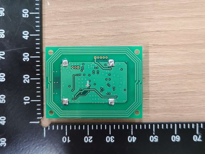
SWUDEABM7
Jun 20, 2022DXX
Equipment Class
DXX - Part 15 Low Power Communication Device Transmitter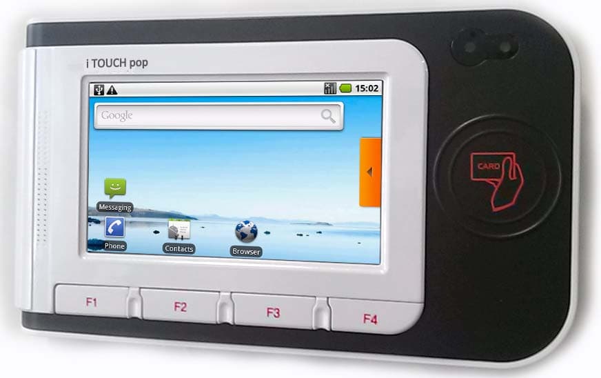
SWUITOUCHPOPV2
Jun 29, 2015SMART CARD READER
Equipment Class
DTS - Digital Transmission System
SWUBLP-A04-NR06
May 28, 2015Smart Card Reader
Equipment Class
DXX - Part 15 Low Power Communication Device Transmitter
SWUDE-632
Aug 27, 2014SMART CARD READER
Equipment Class
DXT - Part 15 Low Power Transceiver, Rx Verified
SWUDE-930
Dec 25, 2012SMART CARD READER
Equipment Class
DXT - Part 15 Low Power Transceiver, Rx Verified