SZF702Running Watch GPS
Compass Systems Corp.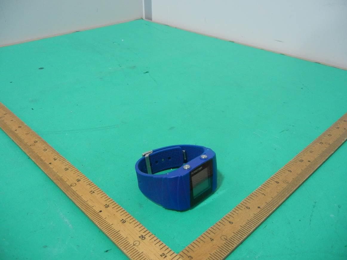
Click to zoom
Application Details
- Equipment Class
- DTS - Digital Transmission System
- Date of Grant
- Dec 16, 2015
- Application Purpose
- Original Equipment
- Date of Application
- Dec 15, 2015
- Equipment Note
- Running Watch GPS
- Frequency Range
- 2402.00000000 - 2480.00000000
- Company
- Compass Systems Corp.
- Country
- Taiwan
Documents & Files
Document Text
Text extracted from the exhibit documents filed with the FCC. Open a document above to read the original.
Cover Letter(s)
1/2 承 承承 承 認 認認 認 書 書書 書 SPECIFICATION FOR APPROVAL 客戶名稱: 鴻方科技股份有限公司 廠 牌: ANTENOVA 料 號: A10192 Apache Communication Inc. 昱博科技股份有限公司 台北市內湖區瑞光路431號2樓 TEL: 886-2-8797-8997 ext:7307 胡玉玫 FAX: 886-2-8797-2929 Mobile Phone: 0937-101-504 承 認 Integrated Antenna Solutions 1 Product Specification 06MD-0002-4-PS Fusca 2.4 GHz SMD Antenna Part No. A10192-L Product Specification 1 Features • Designed for 2.4 GHz applications: Bluetooth ® , Wi-Fi ® (802.11b/g), ZigBee ® , etc. • Easy to integrate • Low profile design for use with no ground beneath the antenna • High efficiency • Light weight • Intended for SMD mounting • Supplied in tape on reel 2 Description Fusca is intended for use with all 2.4 GHz applications. The antenna uses a ground plane in order to radiate efficiently, but this ground plane must not extend underneath the antenna itself. 3 Applications • Mobile phones • PDAs • PNDs • Headsets • PMPs / MP3s • Laptops • PC-Cards • Medical devices • Sensors Fusca 2.4 GHz SMD Antenna Part No. A10192-L Integrated Antenna Solutions 2 Product Specification 06MD-0002-4-PS 4 Part number Fusca: A10192-L 150 5 General data 6 Electrical characteristics Typical performanceConditions Peak gain 0.8 dBi Average gain -1.9 dBi Average efficiency 65% Maximum Return Loss -10 dB Maximum VSWR 2:1 All data measured on Antenova’s reference board, part number AN-1-0549-5 Data given for the 2.4 – 2.5 GHz frequency range Product name Fusca 2.4 GHz Part Number A10192-L Frequency 2.4 – 2.5 GHz Polarization Linear Operating temperature -40 ºC to +85 ºC Impedance with matching 50 Ω Weight < 0.03 g Antenna type SMD Dimensions 4 x 3 x 1.1 [mm] Fusca 2.4 GHz SMD Antenna Part No. A10192-L Integrated Antenna Solutions 3 Product Specification 06MD-0002-4-PS 7 Electrical performance 7-1 Return Loss 2200 2300 2400250026002700 -40 -30 -20 -10 0 ∇ ∇ [MHz] [dB] 7-2 VSWR 22002300 2400250026002700 1 2 3 4 5 ∇ ∇ [MHz] Fusca 2.4 GHz SMD Antenna Part No. A10192-L Integrated Antenna Solutions 4 Product Specification 06MD-0002-4-PS 7-3 Antenna patterns dBi 5 -35 -15 XY plane ZY plane XZ plane Z X Y Patterns show combined polarisations measured on reference board AN-1-0549-5 Fusca 2.4 GHz SMD Antenna Part No. A10192-L Integrated Antenna Solutions 5 Product Specification 06MD-0002-4-PS 8 Antenna dimensions Fusca L W H Length Width Height 4.0 ± 0.2 3.0 ± 0.2 1.1 ± 0.2 Dimensions in mm 9 Antenna footprint Fusca (Part No: A10192-L) * CAD files of the antenna footprint are available from Antenova on request. Please contact [email protected] for further details. I S O J M K L 1.0 ± 0.1 0.8 ± 0.1 ≥0.9 ± 0.1 1.7 ± 0.1 0.6 ± 0.1 2.0 ± 0.1 0.4 ± 0.1 Dimensions in mm Fusca 2.4 GHz SMD Antenna Part No. A10192-L Integrated Antenna Solutions 6 Product Specification 06MD-0002-4-PS 10 Electrical interface 10-1 Transmission lines • All transmission lines should be designed to have a characteristic impedance of 50 Ω • The length of the transmission lines should be kept to a minimum • Any other parts of the RF system like transceivers, power amplifiers, etc, should also be designed to have an impedance of 50 Ω Once the material for the PCB has been chosen (PCB thickness and dielectric constant), a coplanar transmission line can easily be designed using any of the commercial software packages for transmission line design. For the chosen PCB thickness, copper thickness and substrate dielectric constant, the program will calculate the appropriate transmission line width and gaps on either side of the track so the characteristic impedance of the coplanar transmission line is 50 Ω. 10-2 Matching circuit The antenna requires a matching circuit that must be optimized for each customer’s product. The matching circuit will require up to three components and the following pad layout should be designed into the device so the correct circuit can be installed: The antenna feed pad is indicated in the drawing above. Additional pads are for mechanical attachment only and should not be grounded. Fusca 2.4 GHz SMD Antenna Part No. A10192-L Integrated Antenna Solutions 7 Product Specification 06MD-0002-4-PS In addition to the matching circuit, a separate DC blocking capacitor will also be required between the radio and the antenna matching circuit. Note: The component values for the matching circuit will vary depending on the size of the PCB and surrounding components. The impedance of the antenna should be measured before selecting suitable matching components. Antenova offers this service on request. Contact [email protected] for further information. 10-3 Antenna placement Antenova strongly recommends placing the antenna near the edge of the board. Maximum antenna performance is achieved by placing the antenna towards one of the corners of the PCB and with the feed point of the antenna as close to same corner of the PCB as possible. Additional ground and components near the antenna should be at a distance of at least 2 mm. Where possible the antenna should be clear of ground from both sides, although the antenna can work well with a minimum clearance of D ≥ 2 mm as shown in the drawing above. Fusca 2.4 GHz SMD Antenna Part No. A10192-L Integrated Antenna Solutions 8 Product Specification 06MD-0002-4-PS 10-4 Reference boards The reference board has been designed for evaluation purposes of Fusca 2.4 GHz and it includes a SMA female connector Fusca Dimensions in mm To order a reference board contact [email protected] Fusca 2.4 GHz SMD Antenna Part No. A10192-L Integrated Antenna Solutions 9 Product Specification 06MD-0002-4-PS 11 Soldering This antenna is suitable for lead free soldering. The reflow profile should be adjusted to suit the device, oven and solder paste, while observing the following conditions: - The maximum temperature should not exceed 240 ºC - The antenna should not be exposed to temperatures exceeding 120 ºC more than 3 times during the soldering process. 12 Hazardous material regulation conformance The antenna has been tested to conform to RoHS requirements. A…
Text truncated - open the document above for the full version.
External Photos
CERPASS TECHNOLOGY CORP. Report No.: 1511163 Cerpass Technology Corp. Issued Date : Dec. 08, 2015 Page No. : 1 of 7 Photographs of EUT
ID Label/Location Info
–
Internal Photos
CERPASS TECHNOLOGY CORP. Report No.: 1511163 Cerpass Technology Corp. Issued Date : Dec. 08, 2015 Page No. : 2 of 7 CERPASS TECHNOLOGY CORP. Report No.: 1511163 Cerpass Technology Corp. Issued Date : Dec. 08, 2015 Page No. : 3 of 7 CERPASS TECHNOLOGY CORP. Report No.: 1511163 Cerpass Technology Corp. Issued Date : Dec. 08, 2015 Page No. : 4 of 7 CERPASS TECHNOLOGY CORP. Report No.: 1511163 Cerpass Technology Corp. Issued Date : Dec. 08, 2015 Page No. : 5 of 7 CERPASS TECHNOLOGY CORP. Report No.: 1511163 Cerpass Technology Corp. Issued Date : Dec. 08, 2015 Page No. : 6 of 7 CERPASS TECHNOLOGY CORP. Report No.: 1511163 Cerpass Technology Corp. Issued Date : Dec. 08, 2015 Page No. : 7 of 7
RF Exposure Info
CERPASS TECHNOLOGY CORP. Report No.: 1511163 Cerpass Technology Corp. Issued date : Dec. 10, 2015 Page No. : 1 of 2 FCC ID : SZF702 Radio Frequency Exposure LIMIT According to §15.247(i), systems operating under the provisions of this section shall be operated in a manner that ensures that the public is not exposed to radio frequency energy levels in excess of the Commission's guidelines. See § 1.1307(b)(1) of this chapter. EUT Specification EUT Running Watch GPS Frequency band (Operating) WLAN: 2.412GHz ~ 2.462GHz WLAN: 5.150GHz ~ 5.250GHz WLAN: 5.725GHz ~ 5.850GHz Bluetooth: 2.402GHz ~ 2.480 GHz Zigbee: 2.405GHz ~ 2.480 GHz Device category Portable (<20cm separation) Mobile (>20cm separation) Exposure classification Occupational/Controlled exposure (S = 5mW/cm 2 ) General Population/Uncontrolled exposure (S=1mW/cm 2 ) Antenna diversity Single antenna Multiple antennas Tx diversity Rx diversity Tx/Rx diversity Max. output power GFSK: -9.55dBm(0.11mW) Antenna gain (Max) 0.8 dBi Evaluation applied MPE Evaluation* SAR Evaluation N/A Remark: 1. The maximum average output power is -9.55 dBm (0.11mW) at 2402MHz (with numeric 0.8dBi antenna gain.) 2. DTS device is not subject to routine RF evaluation; MPE estimate is used to justify the compliance. 3. For mobile or fixed location transmitters, no SAR consideration applied. The maximum power density is 1.0 mW/cm 2 even if the calculation indicates that the power density would be larger. *Note: Simultaneous transmission is not applicable for this EUT. CERPASS TECHNOLOGY CORP. Report No.: 1511163 Cerpass Technology Corp. Issued date : Dec. 10, 2015 Page No. : 2 of 2 FCC ID : SZF702 TEST RESULTS According to KDB 447498 section 4.3.1, the 1-g SAR test exclusion thresholds at test separation distance ≤ 50 mm are determined by: [(max. power of channel, including tune-up tolerance, mW) / (min. test separation distance, mm)] · [√f(GHz)] ≤ 3.0 The max. average power of channel, including tune-up tolerance(mW) is 0.11mW @ 2402MHz (With Tune-up tolerance), The min. test separation distance (mm) is 5 mm, So, [(max. power of channel, including tune-up tolerance, mW) / (min. test separation distance, mm)] ·[√f(GHz)] = 0.03< 3.0 (With Tune-up tolerance). Therefore, standalone SAR measurements are not required for both head and body.
Test Report
CERPASS TECHNOLOGY CORP. Report No.: TEFQ1511163 Cerpass Technology Corp. Issued Date : Dec. 09, 2015 Page No. : 1 of 40 FCC ID : SZF702 FCC RADIO TEST REPORT Applicant : COMPASS SYSTEMS CORP. Address : 6F, No.413, Sec.2, Ti-Ding Blve., Neihu Dist., Taipei,114 Taiwan R.O.C. Equipment : Running Watch GPS Model No. : RUNNER 301 Trade Name : AVID FIT FCC ID : SZF702 I HEREBY CERTIFY THAT : The sample was received on Nov. 30, 2015 and the testing was carried out on Dec. 03, 2015 at Cerpass Technology Corp. The test result refers exclusively to the test presented test model / sample. Without written approval of Cerpass Technology Corp., the test report shall not be reproduced except in full. Approved by: Tested by: Steven Wang Manager Spree Yei Engineer Laboratory Accreditation: Cerpass Technology Corporation Test Laboratory Cerpass Technology(SuZhou) Co., Ltd. CERPASS TECHNOLOGY CORP. Report No.: TEFQ1511163 Cerpass Technology Corp. Issued Date : Dec. 09, 2015 Page No. : 2 of 40 FCC ID : SZF702 Contents 1. Summary of Test Procedure and Test Results ................................................................................. 5 1.1 Applicable Standards ................................................................................................................. 5 2. Test Configuration of Equipment under Test ................................................................................... 6 2.1 Feature of Equipment under Test ............................................................................................... 6 2.2 Carrier Frequency of Channels .................................................................................................. 7 2.3 Test Mode & Test Software ........................................................................................................ 7 2.4 Description of Test System ......................................................................................................... 7 2.5 General Information of Test ........................................................................................................ 8 3. Test Equipment and Ancillaries Used for Tests ............................................................................... 9 4. Antenna Requirements ..................................................................................................................... 10 4.1 Standard Applicable ................................................................................................................. 10 4.2 Antenna Construction and Directional Gain ............................................................................. 10 5. Test of Conducted Emission ............................................................................................................ 11 5.1 Test Limit .................................................................................................................................. 11 5.2 Test Procedures ....................................................................................................................... 11 5.3 Typical Test Setup .................................................................................................................... 12 5.4 Test Result and Data of Power Port ......................................................................................... 13 5.5 Test Photographs of Power Port .............................................................................................. 15 6. Test of Spurious Emission (Radiated) ............................................................................................ 16 6.1 Test Limit .................................................................................................................................. 16 6.2 Test Procedures ....................................................................................................................... 16 6.3 Typical Test Setup ................................................................................................................... 17 6.4 Test Result and Data (9kHz ~ 30MHz)..................................................................................... 18 6.5 Test Result and Data (30MHz ~ 1GHz).................................................................................... 18 6.6 Test Result and Data (Above 1GHz) ........................................................................................ 24 6.7 Restricted Bands of Operation ................................................................................................. 30 6.8 Restrict band emission Measurement Data ............................................................................. 31 6.9 Test Photographs (30MHz ~ 1GHz) ......................................................................................... 32 6.10 Test Photographs (Above 1GHz) ............................................................................................. 33 7. Test of Spurious Emission (Conducted)......................................................................................... 34 7.1 Test Limit .................................................................................................................................. 34 7.2 Test Procedure ......................................................................................................................... 34 7.3 Test Setup Layout .................................................................................................................... 34 7.4 Test Result and Data ................................................................................................................ 34 8. 6dB Bandwidth Measurement Data ................................................................................................. 36 8.1 Test Limit .................................................................................................................................. 36 8.2 Test Procedures .......................…
Text truncated - open the document above for the full version.
Test Setup Photos
CERPASS TECHNOLOGY CORP. Report No.: TEFQ1511163 Cerpass Technology Corp. Issued Date : Dec. 09, 2015 Page No. : 15 of 40 FCC ID : SZF702 5.5 Test Photographs of Power Port Front View Rear View CERPASS TECHNOLOGY CORP. Report No.: TEFQ1511163 Cerpass Technology Corp. Issued Date : Dec. 09, 2015 Page No. : 32 of 40 FCC ID : SZF702 6.9 Test Photographs (30MHz ~ 1GHz) Front View Rear View CERPASS TECHNOLOGY CORP. Report No.: TEFQ1511163 Cerpass Technology Corp. Issued Date : Dec. 09, 2015 Page No. : 33 of 40 FCC ID : SZF702 6.10 Test Photographs (Above 1GHz) Front View Rear View
Contact Information
Applicant
stone tsao(Q.A. assistant manager)
Technical Contact
COMPASS SYSTEMS CORP.Stone Tsao
[email protected]886-2-87518598
6F, No.413, Sec.2, Ti-Ding Blve., Neihu · Taiwan
Non-Technical Contact
Cerpass Technology Corp.Delia Feng
[email protected]886-3-3226-888
Test Firm
Cerpass Technology Corporation Test LaboratoryBen Wang
Technical Specifications
| # | Rule Parts | Frequency Range | Power Output |
|---|---|---|---|
| 1 | 15C | 2.40 GHz - 2.48 GHz | 700.00 µW |
Other Applications from Compass Systems Corp.

SZF720
Mar 11, 2015Golf GPS Watch
Equipment Class
DTS - Digital Transmission System
SZF700
Nov 29, 2014RUNNING WATCH GPS
Equipment Class
DTS - Digital Transmission System
SZF1001
Mar 10, 2008Bluetooth speaker phone
Equipment Class
DSS - Part 15 Spread Spectrum Transmitter
SZF3039
Jan 30, 2007GPS Bluetooth Receiver
Equipment Class
DSS - Part 15 Spread Spectrum Transmitter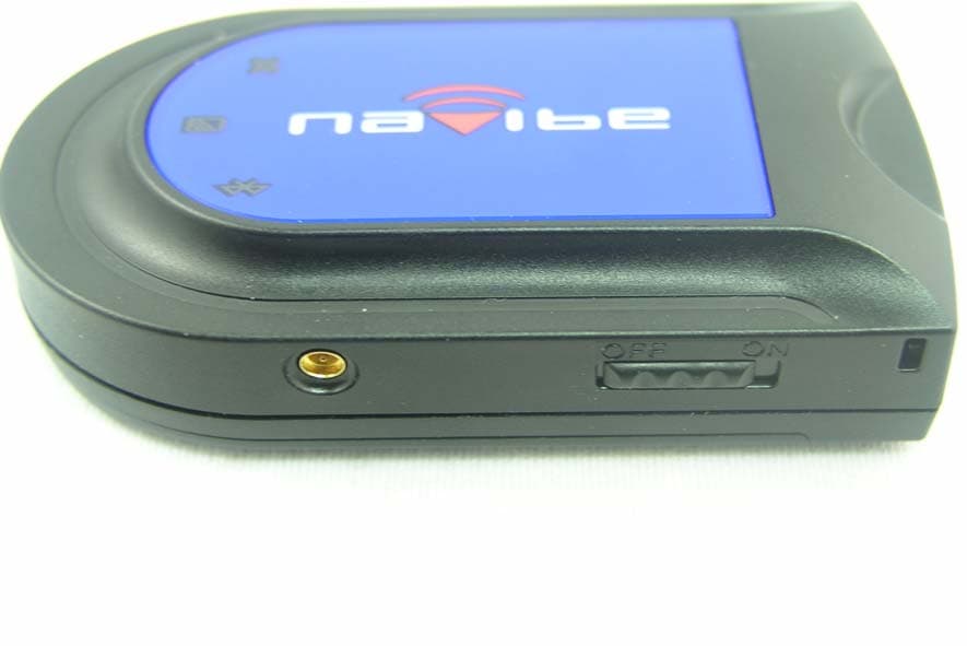
SZF-GB732
Apr 18, 2006Bluetooth GPS Receiver
Equipment Class
DSS - Part 15 Spread Spectrum Transmitter