T9J-RN52Class 2 Bluetooth Module
Microchip Technology Inc.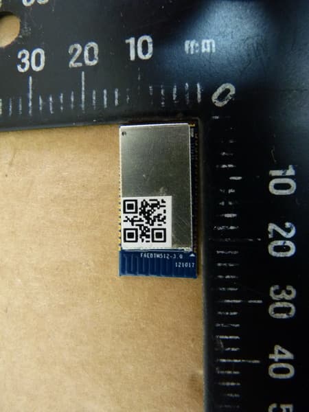
Click to zoom
Application Details
- Equipment Class
- DSS - Part 15 Spread Spectrum Transmitter
- Date of Grant
- Apr 10, 2013
- Application Purpose
- Original Equipment
- Date of Application
- Apr 10, 2013
- Equipment Note
- Class 2 Bluetooth Module
- Frequency Range
- 2402.00000000 - 2480.00000000
- Company
- Microchip Technology Inc.
- Country
- United States
Documents & Files
Document Text
Text extracted from the exhibit documents filed with the FCC. Open a document above to read the original.
Users Manual
www.rovingnetworks.comVersion 1.1 3/19/13page 1 Advanced Information RN52-DS RN52 Bluetooth Audio Module Features: • Fully qualified Bluetooth ® version 3.0 module, fully compatible with Bluetooth version 2.1+EDR, 1.2, and 1.1 • Software configurable through commands over UART console interface • Dedicated GPIO pins enable MCUs to access control and status functions efficiently • Postage-stamp-sized form factor, 13.5 x 26.0 x 2.7 mm • Embedded Bluetooth stack profiles: A2DP, AVRCP, HFP/HSP, and SPP • Dual-channel, differential audio input and output for highest quality audio • Supports iAP profile to discover iOS devices and apps (requires a special firmware build) • Integrated amplifier for driving 16 Ω speakers • UART (SPP) data connection interfaces • External audio CODECs supported via S/PDIF and I 2 S interface • Castellated SMT pads for easy and reliable PCB mounting • Environmentally friendly, RoHS compliant • Certifications: FCC, ICS, CE • Bluetooth SIG certified Applications: • High-quality, 2-channel audio streaming • Wireless stereo headsets • Automotive hands free audio • Wireless audio docking station for smartphones • Wireless speakers • Intercom push-to-talk audio connection • Remote control for media player • Medical devices • Computer accessories RN52 Block Diagram: PCB Antenna Bluetooth 3.0 RF Baseband RN52 UART USB I 2 S S/PDIF 11 GPIO Pins 1 AIO 16-Bit RISC MCU Audio DSP 16-Bit Stereo CODEC 16-MBit Flash 2 LEDs MIC MIC Speaker Speaker www.rovingnetworks.comVersion 1.1 3/19/13page 2 Advanced Information RN52-DS 1.0DEVICE OVERVIEW Roving Network’s RN52 Bluetooth audio module pro- vides a highly integrated solution for delivering high- quality stereo audio in a small form factor. It combines a class 2 Bluetooth radio with an embedded DSP pro- cessor. The module is programmed and controlled with a simple ASCII command language. The RN52 module complies with Bluetooth specifica- tion version 3.0. It integrates RF, a baseband controller, etc., making it a complete Bluetooth subsystem. The RN52 supports a variety of profiles including HSP/HFP, A2DP, AVRCP, SPP, and iAP. It provides a UART inter- face, several user programmable I/O pins, stereo speaker outputs, microphone inputs, and a USB port. Ta b l e 1 -1 provides the general specifications for the module. Ta b l e 1 - 2 and Table 1-3 provide the module’s weight, dimensions, and electrical characteristics. Figure 1-1 shows the module’s dimensions and Figure 1-2 shows recommended landing pattern and layout. TABLE 1-1:GENERAL SPECIFICATIONS SpecificationDescription StandardBluetooth 3.0, class 2 Frequency Band2.4 ~ 2.48 GHz Modulation MethodGFSK, PI/4-DQPSK, 8 DPSK Maximum Data Rate3 Mbps RF Input Impedance50 ohms InterfaceUART, GPIO, AIO, USB, SPI, speaker, microphone Operation Range10 meters (33 feet) Sensitivity-85 dBm at 0.1 % BER RF TX Power4 dBm TABLE 1-2:WEIGHT & DIMENSIONS SpecificationDescription Dimensions26.0 mm x 13.5 mm x 2.7 mm Weight1.2 g TABLE 1-3:ELECTRICAL CHARACTERISTICS SpecificationDescription Supply Voltage3.0 ~ 3.6 V DC Working currentDepends on profiles, 30 mA typical Standby current (disconnected)< 0.5 mA Temperature-40ºC to +85ºC ESDJESD22-A224 class 0 product Humidity10% ~ 90% non-condensing www.rovingnetworks.comVersion 1.1 3/19/13page 3 Advanced Information RN52-DS FIGURE 1-1:MODULE DIMENSIONS FIGURE 1-2:RECOMMENDED PCB FOOTPRINT 0.002.550.853.754.956.157.358.559.75 10.9512.6513.50 0.0 26.00 PCB Outline: +/- 0.13 mm PCB Thickness: +/- 0.100 mm Tolerances: (Top View) Dimensions are in millimeters 21.20 21.40 20.00 18.80 17.60 16.40 15.20 14.00 12.80 11.60 10.40 9.20 8.00 6.80 5.60 4.40 3.20 2.00 (Side View) 26.00 21.40 0.70 0.00 0.000.802.70 0.7512.75 0.8mm 1.6mm 0.80mm Dimensions are in millimeters 0.002.550.853.754.956.157.358.559.75 10.9512.6513.50 0.0 26.00 21.20 21.40 20.00 18.80 17.60 16.40 15.20 14.00 12.80 11.60 10.40 9.20 8.00 6.80 5.60 4.40 3.20 2.00 3.254.656.057.458.8510.25 20.70 Ground Pads 0.8 x 1.0 mm Host Ground Plane Edge (See Mounting Details) (Top View) www.rovingnetworks.comVersion 1.1 3/19/13page 4 Advanced Information RN52-DS Figure 1-3 shows the pinout and Ta b l e 1 - 4 describes the module’s pins. FIGURE 1-3:PIN DIAGRAM RN52 Top View GNDGPIO7GPIO6PWRENVDDPCM_INPCM_OUTPCM_SYNCPCM_CLKGND GND GPIO3 GPIO2 AICO0 GPIO4 GPIO5 GPIO12 GPIO13 GPIO11 GPIO10 GPIO9 USBD- USBD+ UART_RTS UART_CTS UART_TX UART_RX GND SPKR_L+ SPKR_R+ SPKR_L- SPKR_R- AGND MIC_R- MIC_L- MIC_R+ MIC_L+ MIC_BIAS LED0 LED1 SPI_MOSI SPI_SCK SPI_MISO SPI_SS GNDGNDGNDGNDGNDGND 1 2 3 4 5 6 7 8 9 10 11 12 13 14 15 16 17 44 43 42 41 40 39 38 37 36 35 34 33 32 31 30 29 28 18192021222324252627 504948474645 TABLE 1-4:PIN DESCRIPTION (PART 1 OF 3) Note 1 PinSymbolI/O TypeDescriptionDirectionDefault 1GNDGround.Ground. 2GPIO3Bidirectional with program- mable strength internal pull-up/down. This pin enters device firmware update (DFU) mode at bootup if a USB device powers VBUS. GPIO3 requires 47 kΩ to ground and 22 kΩ to the USB VBUS signal if the USB VBUS is supply- ing power to the main board. InputLow 3GPIO2Bidirectional with program- mable strength internal pull-up/down. Reserved, event register. Toggles from high to low for 100 ms to indicate that the module’s state has changed. A microcontroller can enter com- mand mode and poll the state register using the Q action command. OutputHigh 4AIO0Bidirectional.Analog programmable input/output line.I/O 5GPIO4Bidirectional with program- mable strength internal pull-up/down. Factory reset mode. To reset the module to the factory defaults, GPIO4 should be high on power-up and then toggle low, high, low, high with a 1 second wait between the transitions. InputLow www.rovingnetworks.comVersion 1.1 3/19/13page 5 Advanced Information RN52-DS 6GPIO5Bidirectional with program- mable strength internal pull-up/down. Programmable I/O.I/OHigh 7GPIO12Bidirectional with program- mable strength internal pull-up/down. Programmable I/O.I/OHigh 8GPIO13Bidirectional with program- mable strength…
Text truncated - open the document above for the full version.
External Photos
Registration number: W6M21301-13004-C-1 FCC ID: T9J-RN52 Worldwide Testing Services(Taiwan) Co., Ltd. Appendix Page 35 of 38 EUT Photos
Internal Photos
Registration number: W6M21301-13004-C-1 FCC ID: T9J-RN52 Worldwide Testing Services(Taiwan) Co., Ltd. Appendix Page 36 of 38 Registration number: W6M21301-13004-C-1 FCC ID: T9J-RN52 Worldwide Testing Services(Taiwan) Co., Ltd. Appendix Page 37 of 38
RF Exposure Info
MPE Prediction FCC Rule: 15.247(b)(5) Systems operating under the provisions of this section shall be operated in a manner that ensures that the public is not exposed to radio frequency energy levels in excess of the Commission’s guidelines. See §1.1307(b)(1) of this Chapter. LIMITS FOR MAXIMUM PERMISSIBLE EXPOSURE (MPE) Frequency Range (MHz) Electric Field Strength (V/m) Magnetic Field Strength (A/m) Power Density (mW/cm2) Average time (minutes) (A)Limits For Occupational / Control Exposures 30-300 61.4 0.613 1.0 6 300-1500 ... ... F/300 6 1500-100,000 ... ... 5 6 (B)Limits For General Population / Uncontrolled Exposure 30-300 27.5 0.073 0.2 30 300-1500 ... ... F/1500 30 1500-100,000 ... ... 1.0 30 F = Frequency in MHz Prediction of MPE limit at a given distance Equation from page 18 of OET Bulletin 65, Edition 97-01 PG S = -------------- 4πR² where: S = power density P = power input to the antenna G = power gain of the antenna in the direction of interest relative to an isotropic radiator R = distance to the center of radiation of the antenna Maximum peak output power at antenna input terminal: 5.85 (dBm) Maximum peak output power at antenna input terminal: 3.84595 (mW) Antenna gain(maximal): 0 (dBi) Prediction distance: 20 (cm) Prediction frequency: 2402 (MHz) MPE limit for uncontrolled exposure at prediction frequency: 1.0 (mW/cm²) Power density at prediction frequency: 0.000765 (mW/cm²)
Test Report
of Applicant: Microchip Technology Inc. Address: 2355 West Chandler Blvd. Chandler, Arizona, United States 85224-6199 Tested and Prepared by Worldwide Testing Services (Taiwan) Co., Ltd. FCC Registration No.: 930600 Industry Canada filed test laboratory Reg. No. IC 5679A-1 A2LA Accredited No.: 2732.01 Report No.: W6M21301-13004-C-1 6F, NO. 58, LANE 188, RUEY-KUANG RD., NEIHU TAIPEI 114, TAIWAN, R.O.C. TEL: 886-2-66068877 FAX: 886-2-66068879 E-mail: [email protected] FCC PART 15 SUBPART C TEST REPORT for Class 2 Bluetooth Module Model No.: RN52 FCC ID: T9J-RN52 Registration number: W6M21301-13004-C-1 FCC ID: T9J-RN52 Worldwide Testing Services(Taiwan) Co., Ltd. Page 1 of 47 TABLE OF CONTENTS 1 GENERAL INFORMATION .........................................................................................................2 1.1 Notes .....................................................................................................2 1.2 Testing laboratory .....................................................................................................3 1.2.1 Location...........................................................................................................................3 1.2.2 Details of accreditation status.........................................................................................3 1.3 Details of approval holder .....................................................................................................3 1.4 Application details .....................................................................................................4 1.5 General information of Test item............................................................................................4 1.6 Test standards .....................................................................................................5 2 TECHNICAL TEST .......................................................................................................................6 2.1 Summary of test results .....................................................................................................6 2.2 Test environment .....................................................................................................6 2.3 Test Equipment List .....................................................................................................7 2.4 General Test Procedure 11 3 TEST RESULTS (ENCLOSURE) ............................................................................................13 3.1 Peak Output Power (transmitter) 14 3.2 RF Exposure Compliance Requirements 18 3.3 Out of Band Radiated Emissions 18 3.4 Transmitter Radiated Emissions in restricted Bands 19 3.5 Spurious emissions (tx) 20 3.6 Carrier Frequency Separation 23 3.7 Number of Hopping Frequencies 26 3.7.1 Pseudorandom Frequency Hopping Sequence .............................................................28 3.7.2 Coordination of hopping sequences to other transmitters ............................................28 3.7.3 System Receiver Hopping Capability ............................................................................28 3.8 Time of Occupancy (Dwell Time) 29 3.9 20dB Bandwidth 35 3.9.1 System Receiver Input Bandwidth .................................................................................38 3.10 Band-edge Compliance of RF Emissions 39 3.11 Radiated Emissions from Receiver Part 44 3.12 Power Line Conducted Emission 47 Registration number: W6M21301-13004-C-1 FCC ID: T9J-RN52 Worldwide Testing Services(Taiwan) Co., Ltd. Page 2 of 47 1 General Information 1.1 Notes The purpose of conformity testing is to increase the probability of adherence to the essential requirements or conformity specifications, as appropriate. The complexity of the technical specifications, however, means that full and thorough testing is impractical for both technical and economic reasons. Furthermore, there is no guarantee that a test sample which has passed all the relevant tests conforms to a specification. Neither is there any guarantee that such a test sample will interwork with other genuinely open systems. The existence of the tests nevertheless provides the confidence that the test sample possesses the qualities as maintained and that is performance generally conforms to representative cases of communications equipment. The test results of this test report relate exclusively to the item tested as specified in 1.5. The test report may only be reproduced or published in full. Reproduction or publication of extracts from the report requires the prior written approval of the Worldwide Testing Services(Taiwan) Co., Ltd. Tester: February 07, 2013 Leon Chueh Date WTS-Lab. Name Signature Technical responsibility for area of testing: February 07, 2013 Danny Sung Date WTS Name Signature Registration number: W6M21301-13004-C-1 FCC ID: T9J-RN52 Worldwide Testing Services(Taiwan) Co., Ltd. Page 3 of 47 1.2 Testing laboratory 1.2.1 Location OATS No.5-1, Lishui, Shuang Sing Village, Wanli Dist., New Taipei City 207, Taiwan (R.O.C.) 3 meter semi-anechoic chamber No.35, Aly. 21, Ln. 228, Ankang Rd., Neihu Dist., Taipei City 114, Taiwan (R.O.C.) TEL:886-2-6613-0228 FAX:886-2-2791-5046 Company Worldwide Testing Services(Taiwan) Co., Ltd. 6F, NO. 58, LANE 188, RUEY-KUANG RD. NEIHU, TAIPEI 114, TAIWAN R.O.C. Tel : 886-2-66068877 Fax : 886-2-66068879 1.2.2 Details of accreditation status Accredited testing laboratory A2LA accredited number: 2732.01 FCC filed test laboratory Reg. No. 930600 Industry Canada filed test laboratory Reg. No. IC 5679A-1 Test location, where different from Worldwide Testing Services (Taiwan) Co., Ltd. : Name: ./. Accredited number: ./. Street: ./. Town: ./. Country: ./. Telephone: ./. Fax: ./. 1.3 Details of approval holder Name: Microchip Technology Inc. Street: 2355 West Chandler Blvd. Town: Chandler, Arizona, Country: United States 85224-6199 Telephone: (480) 792-7200 Fax: (480) 899-9210 Registration number: W6M21301-13004-C-1 FCC ID…
Text truncated - open the document above for the full version.
Test Setup Photos
Registration number: W6M21301-13004-C-1 FCC ID: T9J-RN52 Worldwide Testing Services(Taiwan) Co., Ltd. Appendix Page 38 of 38 Set Up Photo of Radiated Emission
Contact Information
Applicant
Steve Caldwell
Technical Contact
Worldwide Testing Services (Taiwan) Co., Ltd.Tse-Ming Chang
[email protected]+886-2-6606-8877
6F., No. 58, Lane 188, Ruey Kuand Rd. · Taipei · Taiwan
Test Firm
Worldwide Testing Services (Taiwan) Co., Ltd.Rex Kao
Technical Specifications
| # | Rule Parts | Frequency Range | Power Output |
|---|---|---|---|
| 1 | 15C | 2.40 GHz - 2.48 GHz | 3.85 mW |
Other Applications from Microchip Technology Inc.
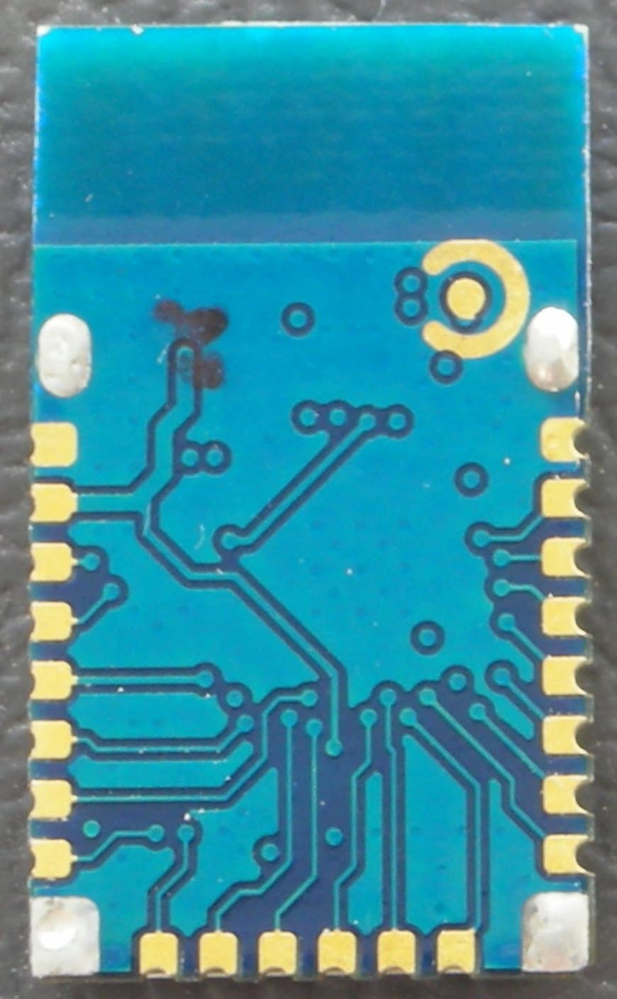
T9JRN4020
May 24, 20142.4GHz BLE MODULE
Equipment Class
DTS - Digital Transmission System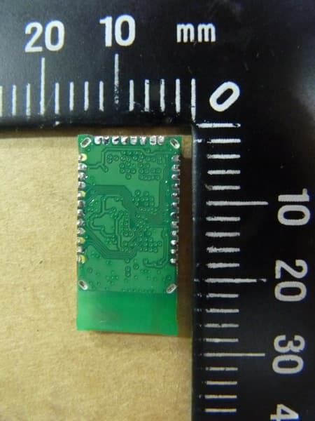
T9JRN41-3
May 28, 2013Class 1 Bluetooth Module
Equipment Class
DSS - Part 15 Spread Spectrum Transmitter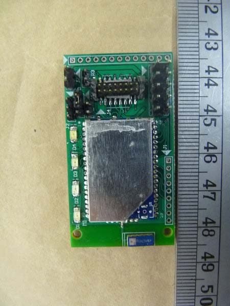
T9J-RN171
Mar 19, 2011WIFLY
Equipment Class
DTS - Digital Transmission System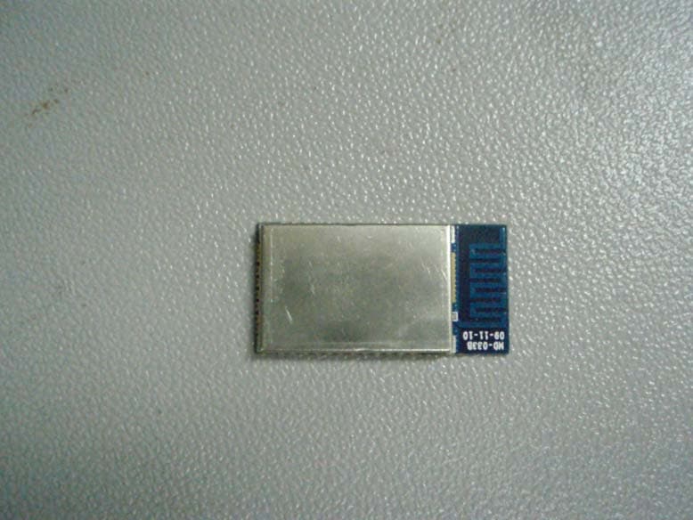
T9J-RN42
Apr 15, 2010RN-42
Equipment Class
DSS - Part 15 Spread Spectrum TransmitterT9J-RN24
Mar 22, 2009Bluetooth Module
Equipment Class
DSS - Part 15 Spread Spectrum Transmitter