TLDSPS-TSFINGERPRINT ACCESS CONTROL READER
Cogent Systems Inc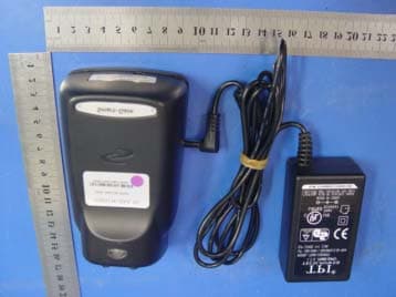
Click to zoom
Application Details
- Equipment Class
- DXX - Part 15 Low Power Communication Device Transmitter
- Date of Grant
- Mar 20, 2006
- Application Purpose
- Original Equipment
- Date of Application
- Mar 20, 2006
- Equipment Note
- FINGERPRINT ACCESS CONTROL READER
- Frequency Range
- 13.56000000 - 13.56000000
- Company
- Cogent Systems Inc
- Country
- United States
Documents & Files
Document Text
Text extracted from the exhibit documents filed with the FCC. Open a document above to read the original.
Users Manual
209 Fair Oaks Avenue South Pasadena, CA 91030 tel: (626) 799-8090 fax: (626) 799-8996 Smart Gate Installation Guide FCC ID : TLDSPS-TS THIS DEVICE COMPLIES WITH PART 15 OF THE FCC RULES. OPERATION IS SUBJECT TO THE FOLLOWING TWO CONDITIONS. (1) THIS DEVICE MAY NOT CAUSE HARMFUL INTERFERENCE AND (2) THIS DEVICE MUST ACCEPT ANY INTERFERENCE RECEIVED , INCLUDING INTERFERENCE THAT MAY CAUSE UNDESIRED OPERATION. 209 Fair Oaks Avenue South Pasadena, CA 91030 tel: (626) 799-8090 fax: (626) 799-8996 FCC Compliance and Advisory Statement This device complies with Part 15 of the FCC rules. Operation is subject to the following two conditions: 1) this device may not cause harmful interference, and 2) this device must accept any interference received, including interference that may cause undesired operation. This equipment has been tested and found to comply with the limits for a Class B digital device, according to Part 15 of the FCC rules. These limits are designed to provide reasonable protection against harmful interference in a residential installation. This equipment generates, uses and can radiate radio frequency energy and if not installed and used in accordance with the instructions, may cause harmful interference to radio communications. However, there is no guarantee that interference will not occur in a particular installation. If this equipment does cause harmful interference to radio or television reception, which can be determined by turning the equipment off and on, the user is encouraged to try correct the interference by one or more of the following measures: 1.Reorient the receiving antenna. 2.Increase the separation between the equipment and receiver. 3.Connect the equipment into and outlet on a circuit different from that to which the receiver is connected. 4.Consult the dealer or an experienced radio/TV technician for help. Any special accessories needed for compliance must be specified in the instruction manual. Warning: A shielded-type power cord is required in order to meet FCC emission limits and also to prevent interference to the nearby radio and television reception. It is essential that only the supplied power cord be used. Use only shielded cables to connect I/O devices to this equipment. CAUSION: Any changes or modifications not expressly approved by the party responsible for compliance could void your authority to operate the equipment. 209 Fair Oaks Avenue South Pasadena, CA 91030 tel: (626) 799-8090 fax: (626) 799-8996 Table of Content 1. Products Description3 2. Accessories4 3. Installation5 4. User Instruction8 5. Specification14 209 Fair Oaks Avenue South Pasadena, CA 91030 tel: (626) 799-8090 fax: (626) 799-8996 1, Product Description Plastic Housing Standard Features Standard features of Smart Gate are: 500 DPI silicon fingerprint sensor Magnetic stripe card reader Standalone or networked operation Configurable security levels Remote configuration through network connection or local configuration through RS232 10/100 Base-T Ethernet connections for communication with a central database and/or administrative software 1:1 authentication or 1:N identification Wiegand output Relay drive output 209 Fair Oaks Avenue South Pasadena, CA 91030 tel: (626) 799-8090 fax: (626) 799-8996 Optional Features The following configurations and optional features are available from the Smart Gate range of terminals: Central administration and database software Contact (ISO 7816) Contact less (MiFare™ 14443A) smart card Match-On-Card Memory upgrade for storage of up to 6,000+ fingerprints Server matching using Ethernet connection 2, Accessories: 1. DB15 Cable 1Ea 2. USB Cable 1Ea 3. Screws, Security 4Ea For Plastic Housing FM3X12 For Aluminum Housing FM4X14 4. Screw Driver 1Ea For Plastic Housing T10 5. Installation Guide 1Ea 6. Warranty Card 1Ea 209 Fair Oaks Avenue South Pasadena, CA 91030 tel: (626) 799-8090 fax: (626) 799-8996 3, Installation 209 Fair Oaks Avenue South Pasadena, CA 91030 tel: (626) 799-8090 fax: (626) 799-8996 Tips for Plastic Housing: 1. Plug the main device all the way in from above the back panel 5 cm height, then push down make sure well contact with back panel and lock. 2. Lock the Device by using the security screws provided from factory. 3. Assembly covered plate. 209 Fair Oaks Avenue South Pasadena, CA 91030 tel: (626) 799-8090 fax: (626) 799-8996 4. Smart-Gate User Manual 1 Preparation: 1.1 Make sure the S2 switch is on “Card Management Mode” (Default setting). 1. 2 Connect the Smart Gate with Category 5 network cable to network switch. Please use POE switch if try to use POE features. 1. 3 Connect the Smart Gate with the COM1 of PC by using special serial cable (come with Smart Gate) 1.4 Connect the power (12V DC power supply to pin 13, 11 of DB15 socket if not using POE). 2 How to use: 2.1 Network Setting: 2.1.1 Follow the instruction of Appendix A to complete the setting of Hyper Terminal first, then open Hyper Terminal, choose function 2 ”Configure Network”, default network setting as Picture 1 (Server IP is the PC is using for communicating). Picture 1 2.2 Enroll / Matching: 2.2.1Create Admin Card: The first contactless card had been read will be the Admin card if there were no templates stored in the Smart Gate. There are three working mode 1. Enroll Mode, 2. Delete Mode, 3. Verify Mode and can be changed by presenting the Admin Card. a. The Yellow LED will start to be flashing after power on 15 seconds later, and at this moment the Smart Gate is waiting for setting Admin card. b. Choose a smart contactless card and present it to the front of the Smart Gate, then remove it away, the Smart Gate will beep and enter enroll work mode, please mark the card as Admin card. 2.2.2Enroll Fingerprint / Enroll Mode: the LED indication is Green LED on, Yellow LED flashing. a. present a smart contactless card near to the front of the Smart Gate, the Green LED will flash once then goes off and leave the yellow LED flashing if the Smart Gate read the card succes…
Text truncated - open the document above for the full version.
Block Diagram
() COGENT SYSTEMS (SHENZHEN)INC. Smart-Gate 2.5VDC LDO 3.3VDC 5VDC DC/DC Power Input 12VDC POE Circuit Watchdog, Beeper, Door Control Network Controlle r Flash Card Reade r FingerPrint Sensor RS485,RS232, Wie gand in/out LCD Display Ke y Board SDRAM RJ45 SecurARM Logical Control CPLD :Cogent Systems Inc 209 Fair Oaks Avenue,South Pasadena,CA91030,U.S.A [email protected] : www.cogentsystems.com 086-0755-86013579 086-0755-86013553 [email protected]
External Photos
Spectrum Research & Testing Lab., Inc. No. 101-10, Ling 8, Shan-Tong Li, Chung-Li City, Taoyuan, Taiwan Tel: 886-3-4987684 Fax: 886-3-4986528 Photo Page: 1 of 1 PHOTOS OF EUT
ID Label/Location Info
Sample of FCC ID Label The device is so small that the 2 parts warning statement does not have to go on the device. It will be really hard to read. We remove the 2 parts statement from the device since we already have it in the manual. FCC ID:TLDSPS-TS
Internal Photos
Spectrum Research & Testing Lab., Inc. No. 101-10, Ling 8, Shan-Tong Li, Chung-Li City, Taoyuan, Taiwan Tel: 886-3-4987684 Fax: 886-3-4986528 Photo Page: 1 of 3 PHOTOS OF EUT Spectrum Research & Testing Lab., Inc. No. 101-10, Ling 8, Shan-Tong Li, Chung-Li City, Taoyuan, Taiwan Tel: 886-3-4987684 Fax: 886-3-4986528 Photo Page: 2 of 3 PHOTOS OF EUT Spectrum Research & Testing Lab., Inc. No. 101-10, Ling 8, Shan-Tong Li, Chung-Li City, Taoyuan, Taiwan Tel: 886-3-4987684 Fax: 886-3-4986528 Photo Page: 3 of 3 PHOTOS OF EUT
Operational Description
Spectrum Research & Testing Lab., Inc. No. 101-10, Ling 8, Shan-Tong Li, Chung-Li City, Taoyuan, Taiwan Tel: 886-3-4987684 Fax: 886-3-4986528 FCC ID: TLDSPS-TS Operational Description of equipment The EUT is a card reading system. The EUT adds DC 12V, and it is going to stand-by mode. When a RFID card approach the EUT, the EUT right now detect, meantime, the LED will be flashing. EUT starts immediately to send data to the PC or controlling system. PRODUCT FINGERPRINT ACCESS CONTROL READER MODEL NO. Smart Gate POWER SUPPLY 12V FREQUENCY BAND 13.56MHz NUMBER OF CHANNEL 1 MODULATION TYPE ASK BIT RATE OF TRANSMISSION 105.9kbps ANTENNA TYPE Directly Matched Antenna DUTY CYCLE 100%
Schematics
123456 A B C D 654321 D C B A Title NumberRevisionSize C Date:24-Aug-2005Sheet of File:\\file-server\incoming\4 finger scanner\SA3_40(AB)20041111.DDB.DDBDrawn By: IMG_D1 IMG_D0 IMG_D2 IMG_D3 IMG_D4 IMG_D5 IMG_D6 IMG_D7 DQM0 DQM1 DQM2 DQM3 DQM0 DQM1 DQM2 DQM3 nSDRAS nSDCAS nSDCS0 SDCKE nSDWE nSDRAS nSDCAS nSDCS0 SDCKE nSDWE SDCLK DQM0 IM_S[2] P17 D[8] E4 IM_S[3] N16 D[9] F4 PXTAL A7 PEXTAL D6 SDCLK M16 TXTAL B7 IM_D[0] R12 IM_D[1] P13 IM_D[2] U12 IM_D[3] T13 IM_D[4] R13 IM_S[0] P15 D[18] G3 D[19] H3 IM_D[5] U13 IM_D[6] U14 D[0] D3 D[1] E3 D[2] F1 D[3] G1 IM_D[7] T14 D[4] J1 D[5] K1 D[20] K3 D[21] L3 D[22] M1 nCS[0] G14 D[23] P1 D[24] E2 D[6] M3 D[25] F2 D[26] H4 D[27] J4 D[28] L4 D[29] M4 D[30] N2 D[7] N3 nCS[1] H15 nCS[2] H16 nCS[3] J17 nOE H17 IM_C[1] T16 IM_C[0] R15 IM_C[2] U17 IM_C[3] R16 IO[9]/PSEL[2] T7 A[19] F17 D[31] P2 A[0] B12 A[1] A13 A[2] D12 A[3] C13 A[4] B13 A[20] E14 A[21] F15 A[22] F14 A[23] G15 A[24] G16 IO[24]/nWE[0] A12 IO[25]/nWE[1] B11 IO[26]/nWE[2] C11 IO[27]/nWE[3] D10 IO[7]/PSEL[0] T6 IO[8]/PSEL[1] U6 IO[10]/PAddr[0] R7 IO[11]/PAddr[1] P8 IO[12]/PAddr[2] U7 IO[13]/PWrite T8 IO[14]/PEnable R8 IO[15]/PCLK P9 IO[16]/PData[0] U9 IO[17]/PData[1] T10 IO[18]/PData[2] R10 IO[19]/PData[3] P11 A[5] A14 IO[20]/PData[4] U10 IO[21]/PData[5] T11 A[6] D13 A[7] C14 A[8] A16 A[9] D14 IO[23]/PData[7] P12 A[10] B15 A[11] A17 A[12] B16 A[13] C15 A[14] D16 A[15] D17 A[16] E17 SDCLKo M17 A[17] E15 SDCKE L16 A[18] E16 IO[0] R4 nSDWE N17 nSDCS[0] N15 nSDCS[1] M14 nSDCAS L15 nSDRAS K14 DQM[0] J14 DQM[1] K15 IO[1] P5 IO[2] U4 IO[3] T5 IO[4] R5 IO[5] P6 IO[6] U5 IO[28] A11 DQM[2] K16 IO[29] B10 IO[30] B8 IO[31] C8 DQM[3] L17 D[10] G2 D[11] H2 D[12] K2 D[13] L2 D[14] N4 D[15] N1 D[16] D1 D[17] E1 IM_S[1] N14 IO[22]/PData[6] R11 SecuARM U1ASecurARM-BGA208 SDCLK A0 A1 A2 A3 A4 A5 A6 A7 A8 A9 A10 A11 A12 A13 A14 A15 A16 A17 A18 A19 A20 A21 A22 A23 A24 A11 A12 A13 A14 A15 A16 A17 A18 A19 A20 A21 A23 A24 D0 D1 D2 D3 D4 D5 D6 D7 D8 D9 D10 D11 D12 D13 D14 D15 D16 D17 D18 D19 D20 D21 D22 D23 D24 D25 D26 D27 D28 D29 D30 D31 D0 D1 D2 D3 D4 D5 D6 D7 D8 D9 D10 D11 D12 D13 D14 D15 D16 D17 D18 D19 D20 D21 D22 D23 D24 D25 D26 D27 D28 D29 D30 D31 nCS0 nCS0 nOE nOE SDRAM FLASH R2 33 IO7 IO8 IO10 IO13 IO14 IO15 IO16 IO17 IO18 IO19 IO20 IO21 IO22 IO23 IMG_S0 IMG_S1 IMG_S2 IMG_S3 R4 330 LED_R R5 330 LED_G LED_R LED_G LED_Y SW0 SW1 SW2 R17 330 LED_Y SW3 R1 33 25MCLK IO11 ENEEP 6 EEDO 7 EEDI 8 EECS 10 EESK 9 IRQ0 29 /SRDY 43 ARDY 38 LCLK 42 W/R 36 /CYCLE 35 /LDEV 45 A1 78 A2 79 A3 80 A4 81 A5 82 A6 83 A7 84 A8 85 A9 86 A10 87 A11 88 A12 89 A13 90 A14 91 A15 92 /RD 31 /WR 32 /DATACS 34 /AEN 41 /RDYRTN 46 RESET 30 XTAL1 127 XTAL2 128 IOS0 3 IOS1 4 IOS2 5 D8 76 D9 75 D10 74 D11 73 D12 71 D13 70 D14 69 D0 107 D1 106 D2 105 D3 104 D4 102 D5 101 D6 100 D7 99 /ADS 37 D15 68 D16 66 D17 65 D18 64 D19 63 D20 61 D21 60 D22 59 D23 58 D24 56 D25 55 D26 54 D27 53 D28 51 D29 50 D30 49 D31 48 /BE3 97 /BE2 96 /BE1 95 /BE0 94 X25OUT 47 /CSOUT 2 /VLBUS 40 U15ALAN91C111-TQFP A2 A3 NT_nRD NT_nWR NT_IRQ NT_AEN IO8 IO10 IO11 EN485T IO13 IO14 IO15 IO16 IO17 IO18 IO19 IO20 IO21 IO22 25MCLK nCS1 CS 1 SK 2 DI 3 DO 4 VCC 8 NC 7 NC 6 GND 5 U11 FM93C46LM8 3V3 nRESA nRES nSRST NT_RES TDO_CPLD nCS1 DQM0 IO7 IO23 1 2 3 4 5 6 7 8 9 10 11 12 13 14 15 16 J8 FH10A-16S-1SH(1.0) IMG_S1 SCL IM1_C1 5V D0 D1 D2 D3 D4 D5 D6 D7 D8 D9 D10 D11 D12 D13 D14 D15 3V3 A12 4 A13 3 A14 2 A15 1 /CE 26 A20 10 A19 15 A18 16 A17 17 A16 48 Vcc 37 GND 27 DQ6 42 DQ14 43 DQ7 44 DQ15 45 /OE 28 /WE 11 /WP 14 DQ13 41 DQ5 40 DQ12 39 DQ4 38 A21 9 VccQ 47 DQ11 36 DQ3 35 DQ10 34 DQ2 33 A0 25 DQ0 29 DQ8 30 DQ1 31 DQ9 32 A8 8 GND 46 A7 18 A6 19 A5 20 A4 21 A3 22 A2 23 A1 24 A9 7 A10 6 A11 5 R/nP 12 Vpp 13 U4 TE28F160C3BC90 A1 A2 A3 A4 A5 A6 A7 A8 A9 A10 A11 A12 A13 A14 A15 A16 A17 A18 A19 A20 A21 A22 D0 D1 D2 D3 D4 D5 D6 D7 D8 D9 D10 D11 D12 D13 D14 D15 3V3 nOE NT_nRD NT_nWR NT_IRQ NT_AEN NT_RES IMG_D0 IMG_D1 IMG_D2 IMG_D3 IMG_D4 IMG_D5 IMG_D6 IMG_D7 IMG_S0 IMG_S2 IMG_S3 3V3 TDO_ARM TCK TMS R31 25 R32 25 R33 25 R34 25 R35 50 R36 330 R37 330 1 2 D8 1 1 2 2 D9 3V3 R30 11k(1%) 10/100M Vss 24 Vss 57 Vdd 1 Vss 72 Vdd 33 Vdd 44 Vss 52 Vss 39 MCLK 27 /CNTL 28 /LNK 20 LBK 21 TX25 109 AVdd 16 /LEDA 22 /LEDB 23 TPO- 15 TPO+ 14 MDI 25 RXER 126 AVss 13 AVdd 11 RXDV 125 COL100 112 CRS100 119 TXEN100 111 TPI- 18 TPI+ 17 AVss 19 Vss 117 Vdd 120 Vdd 110 MDO 26 Vss 93 RX25 118 Vdd 62 Vss 103 Vdd 98 Vss 108 Vdd 77 RXD0 124 RXD1 123 RXD2 122 RXD3 121 TXD0 116 TXD1 115 TXD2 114 TXD3 113 RBIAS 12 Vss 67 U15BLAN91C111-NE3V3 R38 50 C77 0.01u 3V3 LCD_D0 LCD_D1 LCD_D2 LCD_D3 LCD_D4 LCD_D5 LCD_D6 LCD_D7 LCD_RS3 LCD_RW3 LCD_E3 EN_RELAY WIEGAND1 RX485 RXTTL RX232 RXD0 WIEGAND0 3V3 /EN_5V 3V3 R52 10k 5V R55 47k IM1_C1 A1 IO9 IO12 IO9 IO12PINT PINT R57 330 IM1_DIM1_C1 R3 33 X1 1 X2 2 VBAT 3 GND 4 SDA 5 SCL 6 SQW/OUT 7 VCC 8 U6DS1307 Y1 32.768KHZ 5V C45 12.5pF C44 12.5pF BATT1 CR927 3V 5V R47 4.7k R46 4.7k SDA SCL 1 2 3 4 J12 J_ExtLED(J1.25mm) EXT_R EXT_G 3V3 EXT_Y EXT_R EXT_G EXT_Y OE 1 GND 2 Out 3 Vcc 4 U12 CB3LV-3C-25 3V33V3 25MCLK Beep SDA SCL BA1 23 A0 25 A1 26 A2 27 A3 60 A4 61 A5 62 A6 63 A7 64 A8 65 A9 66 A10 24 BA0 22 DQM0 16 DQM1 71 DQM2 28 DQM3 59 nCS 20 nWE 17 nCAS 18 nRAS 19 CKE 67 CLK 68 DQ31 56 DQ0 2 DQ1 4 DQ2 5 DQ3 7 DQ4 8 DQ5 10 DQ6 11 DQ7 13 DQ8 74 DQ9 76 DQ10 77 DQ11 79 DQ12 80 DQ13 82 DQ14 83 DQ15 85 DQ16 31 DQ17 33 DQ18 34 DQ19 36 DQ20 37 DQ21 39 DQ22 40 DQ23 42 DQ24 45 DQ25 47 DQ26 48 DQ27 50 DQ28 51 DQ29 53 DQ30 54 A11 21 U3AMT48LC4M32B2TG-10 SDRAM A22 IN0/CLK0 90 TCK/IO/MC3-2 62 TDI/IO/MC6-2 4 IN2/CLK2 88 IN3/CLK3 87 IO/MC5-1 2 IO/MC5-2 1 IO/MC5-3 100 IO/MC5-4 99 IO/MC1-3 72 IO/MC5-5 98 IO/MC5-6 97 IO/MC1-4 71 IO/MC5-7 96 IO/MC5-13 94 IO/MC5-14 93 IO/MC1-5 70 IO/MC5-15 92 IO/MC6-3 5 IO/MC1-6 69 IN1/CLK1 89 IO/MC1-11 67 IO/MC1-7 68 IO/MC1-13 65 IO/MC1-14 64 IO/MC1-15 63 IO/MC2-7 81 IO/MC2-1 75 IO/MC2-2 76 IO/MC2-3 77 IO/MC2-4 78 IO/MC2-5 79 IO/MC2-6 80 IO/MC2-11 83 IO/MC2-12 84 IO/MC2-13 85 IO/MC3-3 61 IO/MC3-4 60 IO/MC3-6 58 IO/MC3-7 57 IO/MC3-11 56 IO/MC3-12 55 IO/MC3-13 54 IO/MC3-14 53 I…
Text truncated - open the document above for the full version.
Schematics
123456 A B C D 654321 D C B A Title NumberRevisionSize C Date:24-Aug-2005Sheet of File:\\file-server\incoming\4 finger scanner\SA3_40(AB)20041111.DDB.DDBDrawn By: Input 1 DELAY 2 PWM 3 GND 4 VS 5 Out 6 Flag 7 U2 DRV102 C13 1nF C12 0.1uF D8 MBRS360TR D9 MBRS360TR D6 RED V_BAT V_BAT R12 10K R11 330 V_BAT 1 2 J2 CON2(1.25) Det_Open EN_RELAY_E 1 2 3 4 J11 MINIUSB/F 232TX1 232RX1 RESET1 SA3_EXTENSION SCH 5V nRES_H R13 1k R16 20k + C2 10u/20V C3 0.1uF DRVOUT R1 10k 3V3C15 0.1uF C14 0.1uF C11 0.1uF K4_5 K5_5 K6_5 K7_5 K3_5 K2_5 K1_5 K0_5 GND 5V 1 2 3 4 5 J15 J-ExtMAG(2.54) K5 K6 K7 CLS RCL RDT TXD0GND 5V 1 2 3 4 5 J14 J_ExtIC(2.54) ICRST_5 1 2 3 Q11 2SD602-(TX) R21 10 R8 330 EN_RELAY_E RELAY- R26 1201 2 JP3 485_Jumper WIEGAND1WIEGAND0 1 2 3 Q3 2SD602-(TX) R41 100 R15 330 WIEG0 1 2 3 Q4 2SD602-(TX) R42 100 R27 330 WIEG1 VCCA 1 A1 3 A2 4 A3 5 A4 6 A5 7 A6 8 A7 9 A8 10 DIR 2 /CS 22 VCCB 24 B1 21 B2 20 B3 19 B4 18 B5 17 B6 16 B7 15 B8 14 GND 11 GND 12 GND 13 U7 74LVX3245 3V3 CLS RCL RDTRDT3 RCL3 CLS3 5or3.3V 16 12 13 9 15 10 17 8 C1+ 2 C2+ 5 GND 18 C1- 4 VCC 19 C2- 6 V- 7 EN 1 FORCEOFF 20 FORCEON 14 V+ 3 INVALID 11 U5MAX3223ECAP3V3 12 C490.1u 12 C520.1u 12 C48 0.1u 12 C500.1u 12 C510.1u 3V3 RX232 TXD0 TXD1 1 2 C54 22p 1 2 C53 22p 1 2 C56 22p 1 2 C55 22p 232TX0 232RX0 232TX1 232RX1 Rx 1 /RE 2 DE 3 Tx 4 Vcc 8 B 7 A 6 Gnd 5 U10 LTC1480CS8 3V3 485- 485+TX485 EN485T RX485 3V3 3V3 K4 K5 K6 K7 K4_5 K5_5 K6_5 K7_5 VCCA 1 A1 3 A2 4 A3 5 A4 6 A5 7 A6 8 A7 9 A8 10 DIR 2 /CS 22 VCCB 24 B1 21 B2 20 B3 19 B4 18 B5 17 B6 16 B7 15 B8 14 GND 11 GND 12 GND 13 U6 74LVX3245 3V3 K0_5 K1_5 K2_5 K3_5K3 K2 K1 K0 5or3.3V TXD0_IC ICRST_E TXD0_IC_5 ICRST_5 WiegRX0 WiegRX1 1 2 C57 22p 1 2 C58 22p 1 2 C59 22p 1 2 C60 22p 485+485-WIEG0WIEG1 1 2 3 4 5 6 7 8 J3 KEYPAD R49 20 R48 1K BEEP_E B1 BUZZER/12V V_BAT RXTTL_5RXTTL This Reset will do power cycling Open Box Detection + C19 47u/6.3V 1 2 3 4 BR1 DF01SA 1 2 3 4 BR2 DF01SA NC 1 RClass 2 NC 3 Vin 4 Vout 5 PWRGD 6 SIGDIS 7 GND 8 U1 LTC4257-1 C8 0.1u/100V D3 SMAJ58A TVS D5 S1B D1 S1B Vin 1 FeedBack 4 Output 2 GND 3 On/Off 5 IC1LM2576HVT-12 + C4 47u/100V L1 220u/PE-52626 V_BAT R7 1k 1 1 2 2 D7 RED FUSE1 miniSMD070 C7 0.1uF +12V POE1+ POE1- POE0+ POE0- V_BAT_IN+ +C6 330u/25V R3 100k R4 10k C16 0.1u/100V 123 JP6 CON3 123 JP5 CON3 Vin Vin 12 C17 1000P 12 C18 1000P 12 C21 1000P 12 C22 1000P R51 10K R50 10K R2 10K 3V3 CLS RCL RDT DET_OPEN CLS RCL RDT R9 1%45.3 1 2 3 Q8 2SD602-(TX) 1 2 3 Q2 2SD602-(TX) A/B 1 1A 2 1B 3 1Y 4 2A 5 2B 6 2Y 7 GND 8 3Y 9 3B 10 3A 11 4Y 12 4B 13 4A 14 OE 15 VCC 16 U3SN74LVC157APW RXD0_IC TXD0 RXD0_A RXTTL_5 TXD0_IC_1 TXD0_A RS_SEL 3V3 TXD0_A_5 GND 3V3 5V RXD0_A TXD0_IC_5 RXD0_IC 3V3 RX232_1 LessNormal POE- LessPOE+ Normal K0 K1 K2 K3 K4 K5 K6 K7 RX485 EN485T WIEGAND1WIEGAND0 CLS3 RCL3 RDT3 nRES_H Beep EN_RELAY TXD0 RXTTL ICRST TXD1 RX232_1 RX232 WDG_TRG POE0-POE0+ POE1-POE1+ V_BAT 5V 5or3.3V 12 34 56 78 910 1112 1314 1516 1718 1920 JP2 HEADER 10X2 5V12 34 56 78 910 1112 1314 1516 1718 1920 2122 2324 JP1 HEADER 12X2 RS_SEL 3V3 R19 100 K7 Drv102 1 2 3 4 5 6 J1 J_Sensor(1.27) NTGND + C1 22u/10V C24 0.1uF +C23 330u/25V D2 MBRS360TR BATT1 CR927 3V BATT1 BATT1 + C20 47u/100V A 2 B 3 E 1 Y0 4 Y1 5 Y2 6 Y3 7 VCC 16 GND 8 U8A74HC139 3V3 3V3 Beep ICRST4 5 6 U4B SO-14 8 9 10 U4C 74HC08 EN_RELAY EN_RELAY_S BEEP_S LED_Bar_S EN_RELAY_S EN_RELAY_E BEEP_S BEEP_E LED_Bar_S LED_Bar_E11 12 13 U4D 74HC08 ICRST_S ICRST_E ICRST_S GND LED_Bar_E TXD0_ATXD0_A_5 1 2 3 4 J4 3V3 WDG_TRG 1 2 3 7 7 14 14 U4A 74LS08 TX485 TXD1 R6 0 R10 0 R5 0 Beep ICRST EN_RELAY BEEP_E ICRST_E EN_RELAY_E R14 10k TXD0 L2 BLM21AG102SN1 123 JP4 CON3 Less12VV_BATH12V Less12V VinLess12V 1 2 3 4 5 6 7 8 9 10 11 12 13 14 15 J5 CON15 Wieg_Out_D0 Wieg_In_D0 Wieg_Out_D1 Wieg_In_D1 DRV_Out Wieg GND RS-485(-) RS-485(+) RS-232 TX RS-232 RX Power GND RELAY_2 Power Input RELAY_1 Safety GND WIEG0 CLS WIEG1 RCL NTGND GND DRVOUT 485- 485+ 232TX1 232RX1 GND V_BAT_IN+ V_BAT RELAY- D4BAS16 C9 0.1uF A/B 1 1A 2 1B 3 1Y 4 2A 5 2B 6 2Y 7 GND 8 3Y 9 3B 10 3A 11 4Y 12 4B 13 4A 14 OE 15 VCC 16 U9SN74LVC157APW TXD0_IC_1TXD0_IC EN485T 3V3 3V3 3V3 TXD1TXD1_1 R17 0 R18 0 TXD1_1 TXD1 SA3_40B
Test Report
Spectrum Research & Testing Lab., Inc. No. 101-10, Ling 8, Shan-Tong Li, Chung-Li City, Taoyuan, Taiwan, R.O.C. TEST REPORT Reference No.: A05071507 Report No.: FCCA05071507 FCC ID: TLDSPS-TS Page: 2 of 25 Date: Mar. 06, 2006 Table of Contents 1. DOCUMENT POLICY AND TEST STATEMENT ............................................... 4 1.1 DOCUMENT POLICY ........................................................................................ 4 1.2 TEST STATEMENT............................................................................................ 4 1.3 EUT MODIFICATION ......................................................................................... 4 2. DESCRIPTION OF EUT AND TEST MODE ...................................................... 5 2.1 GENERAL DESCRIPTION OF EUT .................................................................. 5 2.2 DESCRIPTION OF EUT INTERNAL DEVICE ................................................... 5 2.3 DESCRIPTION OF TEST MODE.................................................................... 5 2.4 DESCRIPTION OF SUPPORT UNIT ................................................................. 6 3. DESCRIPTION OF APPLIED STANDARDS ..................................................... 6 4 OCCUPIED BANDWIDTH................................................................................. 7 4.1 TEST EQUIPMENT............................................................................................ 7 4.2 TEST SET-UP .................................................................................................... 7 4.3 TEST PROCEDURE .......................................................................................... 7 4.4 EUT OPERATING CONDITION ......................................................................... 7 4.5 TEST RESULT ................................................................................................... 8 5. CONDUCTED EMISSION TEST ........................................................................ 9 5.1 CONDUCTED EMISSION LIMIT ....................................................................... 9 5.2 TEST EQUIPMENT............................................................................................ 9 5.3 TEST SETUP....................................................................................................10 5.4 TEST PROCEDURE .........................................................................................10 5.5 EUT OPERATING CONDITION ........................................................................10 5.6 TEST RESULT ..................................................................................................11 6. RADIATED EMISSION TEST .......................................................................... 12 6.1 RADIATED EMISSION LIMIT ...........................................................................12 6.2 TEST EQUIPMENT...........................................................................................13 6.3 TEST SETUP....................................................................................................14 6.4 TEST PROCEDURE .........................................................................................16 6.5 EUT OPERATING CONDITION ........................................................................16 6.6 RADIATED EMISSION TEST RESULT ............................................................17 7 FREQUENCY TOLERANCE..............................................................................19 7.1 FREQUENCY TOLERANCE LIMIT ..................................................................19 7.2 TEST EQUIPMENT...........................................................................................19 7.3 TEST PROCEDURES.......................................................................................20 7.4 TEST SETUP....................................................................................................20 Spectrum Research & Testing Lab., Inc. No. 101-10, Ling 8, Shan-Tong Li, Chung-Li City, Taoyuan, Taiwan, R.O.C. TEST REPORT Reference No.: A05071507 Report No.: FCCA05071507 FCC ID: TLDSPS-TS Page: 3 of 25 Date: Mar. 06, 2006 7.5 TEST RESULT ..................................................................................................21 8 PHOTOS OF TESTING......................................................................................22 9. TERMS OF ABRIVATION .................................................................................. 25 Spectrum Research & Testing Lab., Inc. No. 101-10, Ling 8, Shan-Tong Li, Chung-Li City, Taoyuan, Taiwan, R.O.C. TEST REPORT Reference No.: A05071507 Report No.: FCCA05071507 FCC ID: TLDSPS-TS Page: 4 of 25 Date: Mar. 06, 2006 1. DOCUMENT POLICY AND TEST STATEMENT 1.1 DOCUMENT POLICY - The report shall not be reproduced except in full, without the written approval of SRT Lab, Inc. - The report must not be used by the applicant to claim that the product is endorsed by NVLAP, TÜV, NEMKO and SRT. - The NVLAP logo applies only to the applicable standards specified in this report. 1.2 TEST STATEMENT - The test results in the report apply only to the unit tested by SRT Lab. - There was no deviation from the requirements of test standards during the test. - AC( 100-240 Vac50/60 Hz )To DC 12V Adapter, was used during the test. 1.3 EUT MODIFICATION - No modification in SRT Lab. Spectrum Research & Testing Lab., Inc. No. 101-10, Ling 8, Shan-Tong Li, Chung-Li City, Taoyuan, Taiwan, R.O.C. TEST REPORT Reference No.: A05071507 Report No.: FCCA05071507 FCC ID: TLDSPS-TS Page: 5 of 25 Date: Mar. 06, 2006 2. DESCRIPTION OF EUT AND TEST MODE 2.1 GENERAL DESCRIPTION OF EUT PRODUCT Fingerprint Access Control Reader MODEL NO. Smart Gate POWER SUPPLY 12V FREQUENCY BAND 15.63MHz NUMBER OF CHANNEL 1 MODULATION TYPE ASK BIT RATE OF TRANSMISSION105.9kbps ANTENNA TYPE Directly Matched Antenna DUTY CYCLE 100% NOTE : For more detailed information, please refer to the EUT’s…
Text truncated - open the document above for the full version.
Test Setup Photos
Spectrum Research & Testing Lab., Inc. No. 101-10, Ling 8, Shan-Tong Li, Chung-Li City, Taoyuan, Taiwan, R.O.C. TEST REPORT Reference No.:A05071507 Report No.:FCCA05071507 Page: 19 of 22 Date:Oct. 11, 2005 7 PHOTOS OF TESTING - Conducted test : Spectrum Research & Testing Lab., Inc. No. 101-10, Ling 8, Shan-Tong Li, Chung-Li City, Taoyuan, Taiwan, R.O.C. TEST REPORT Reference No.:A05071507 Report No.:FCCA05071507 Page: 20 of 22 Date:Oct. 11, 2005 - Radiated test : 9kHz – 30MHz Spectrum Research & Testing Lab., Inc. No. 101-10, Ling 8, Shan-Tong Li, Chung-Li City, Taoyuan, Taiwan, R.O.C. TEST REPORT Reference No.:A05071507 Report No.:FCCA05071507 Page: 21 of 22 Date:Oct. 11, 2005 - Radiated test : 30MHz – 1000MHz
Contact Information
Applicant
Ankuo Wang(Asia General Manager)
Test Firm
Spectrum Research & Testing Laboratory, Inc.Cheng Ho
Technical Specifications
| # | Rule Parts | Frequency Range | Power Output |
|---|---|---|---|
| 1 | 15C | 13.56 MHz - 13.56 MHz | - |
Other Applications from Cogent Systems Inc
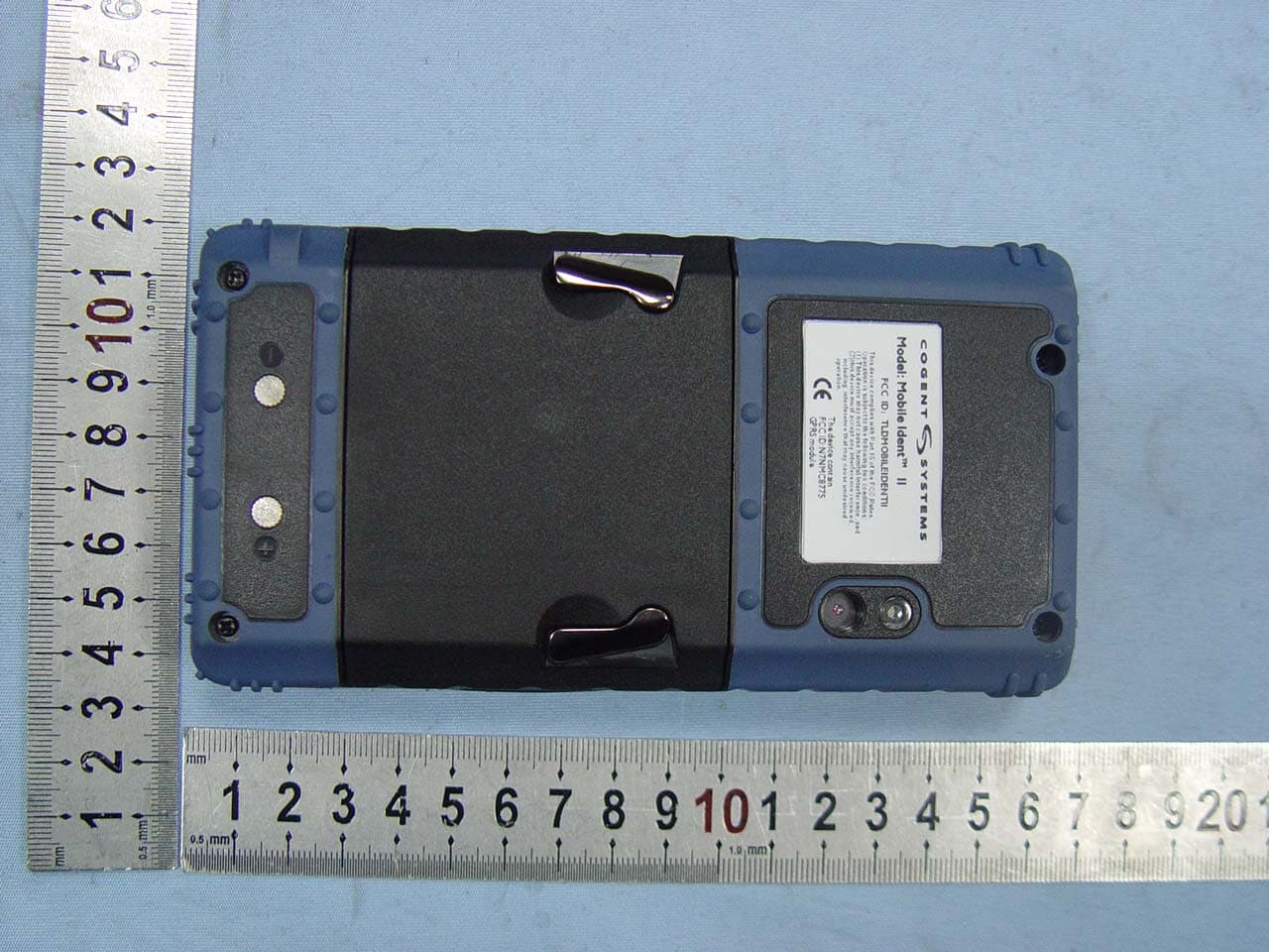
TLDMOBILEIDENTII
Dec 08, 2008Cogent Multifunction Fingerprint Scanner
Equipment Class
DTS - Digital Transmission System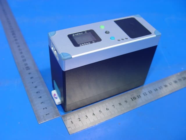
TLDSARII
Nov 18, 2007STAND ALONE READER II
Equipment Class
DSS - Part 15 Spread Spectrum Transmitter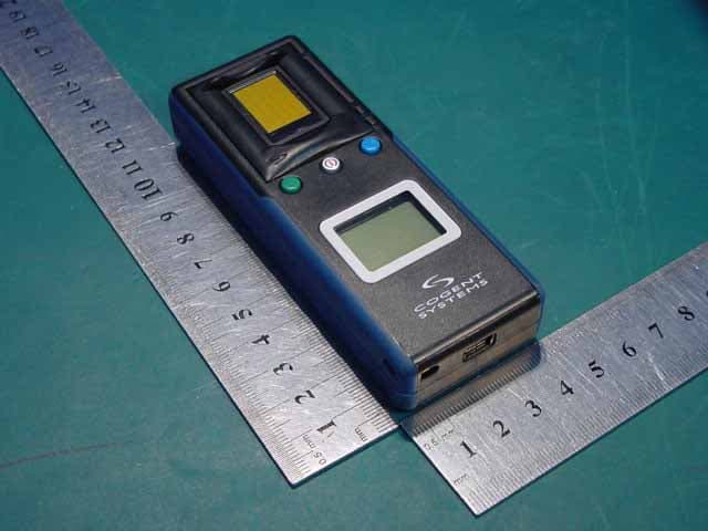
TLDBLUECHECK
Oct 16, 2006Fingerprint capture/identification device w/BT
Equipment Class
DSS - Part 15 Spread Spectrum Transmitter