TRIMD-012.4G module
Meijiaxin Toys Co., Ltd.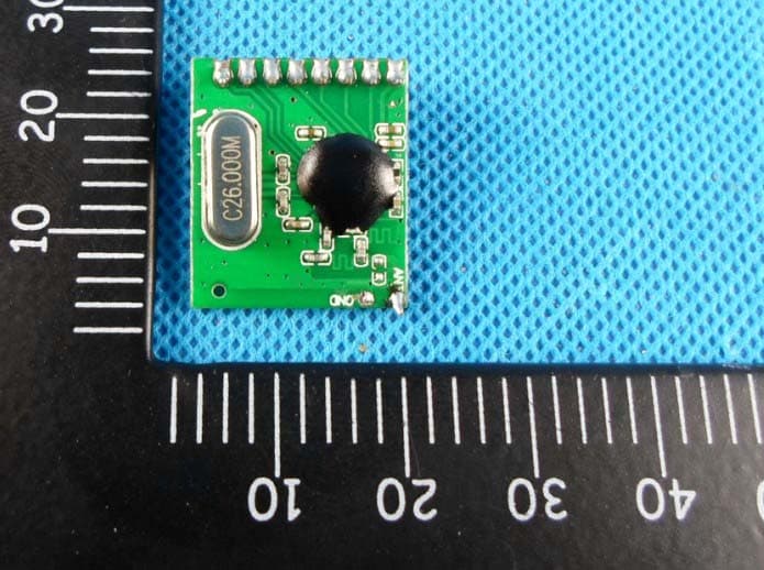
Click to zoom
Application Details
- Equipment Class
- DXX - Part 15 Low Power Communication Device Transmitter
- Date of Grant
- Jul 11, 2012
- Application Purpose
- Original Equipment
- Date of Application
- Jul 11, 2012
- Equipment Note
- 2.4G module
- Frequency Range
- 2413.00000000 - 2472.00000000
- Company
- Meijiaxin Toys Co., Ltd.
- Country
- Hong Kong
Documents & Files
Document Text
Text extracted from the exhibit documents filed with the FCC. Open a document above to read the original.
Users Manual
1、 Overview MD-01 is a low-cost,low-power single-chip RF transceiver module operatingin the 2.4GHz ISM band. MD-01 is designed for a small amount of data designed wireless controller. 2、Features Frequency between the 2400MHz ~ 2483.5MHz; Rate up to 250kbps, and high datathroughput; Has high sensitivity (the rate at 10Kbps under-98dbm, 1% packet error rate) Current consumption is very small, in the receive mode current is15.6mA; Design of the output power up to +1 dbm; Built-in CRC error detection hardware circuits and protocols Support for asynchronous transparent receive and transmit mode,and is compatible with existing wireless communication protocol 3、Principles and external chip module block diagram 4、Description 1)RF receive mode MD-01(MC-01) at VDD = 3.0V, Tc = 25 ° condition, the receiversensitivity is -88dBm at the rate of 250Kbps , 10kbps rate when-98dBm, the digital channel filter bandwidth between the 58~650KHz bandwidth limit should be crystal proportional to the frequency. 2)RF transmit mode MD-01's output power between-30dBm ~ +1 dBm, and spuriousradiation in the frequency of 25MHz ~ 1GHz ,is -36dBm, at 47 ~ 74,87.5 ~ 118,174 ~ 230,470 ~ 862MHz is -54dBm, the 1800MHz ~ 1900MHz (restricted band in Europe) is as-47dBm, and in 2 * RF 3 * RF (U.S. restrictions on the band) when -41dBm, the other is -30dBm when the frequencies above 1GHz. 3)4-wire configuration interface When the MD-01 in a subordinate position, it's SI, SO, SCLK,CSn four port is configured as a simple 4-wire synchronous parallel ports, which are also used as a buffer to read and writedata. All the parallel port data transfer begins with the first byte, includinga read/write signal, the pulse signal and a 6-byte address. During the address and data transmission, CSn pin (chip select,active low) must be kept low. If the transfer to take to CSn high, the transmission will be terminated. When CSn is set low, the microcontroller must wait for theMD-01's low SO pin is set to begin after the first byte transfer, indicating that the voltage regulator has stabilized, crystal work,unless the transfer is completed or the chip in sleep state, CSn pin is set low after the SO pin will be set low. 4)Modulation MD-01 supports amplitude modulation, frequency shift keying and phase shift keying mode a) Amplitude modulation MD-01 supports two different forms of amplitude modulationmode: off keying and amplitude shift keying. Off keyingmodulation, respectively, through simply set to "1" or "0" to turn onor turn off power make a big function, and amplitude shift keyingcan be programmed to adjust to a more sophisticated range ofsizes. b) Frequency Shift Keying FSK symbol coding as follows: c) Phase shift keying Phase shift keying is in transit to maintain a certain Period to transmit data. 5)Wireless Control a) Running order When the power is turned on, the system mustbe reset. In one of two ways must be executed: automatic restart or manual restart From time to time re-configuration is as follows: SCLK set to "1" while SI is set to "0" to avoid pin control modemay arise. Strobe CSn set high At least 40us CSn is high CSn low and wait for SO to be set low, then there is data to send or receive The synchronous reset signal gating When the SO once again set low, the reset is complete and thechip is idle b) Mode MD-01 has two operating modes: receive and send. These patterns through the micro-controller SRX or STX strobecommands to directly activate, or wake up automatically by thewireless. c) Wireless wake-up (WOR) functionality This optional wireless wake-up function can make the MD-01periodically wake up from a deep sleep. This function WOR has twocontrol modes choose to rely on PKTCTRL1.AUTOSYNCbits. When this bit is set to "0", the module will be wireless wake up in the Event0 point in time, and enters the RX State Event1point, which will ensure access to RX state at the exact time. 5、Limit rating Parameter Min Max UnitRemarks Input voltage 1.8 3.6 V All power supply pin have the same voltage input Max output power 1 dbm Max data transfer rate 250 Kbps Operating Temperature -40 85 °C Storage Temperature -50 150 °C 6、Module size and pin description Module size FCC Caution: Any changes or modifications not expressly approved by the party responsible for compliance could void the user's authority to operate this equipment. This device complies with Part 15 of the FCC Rules. Operation is subject to the following two conditions: (1) This device may not cause harmful interference, and (2) this device must accept any interference received, including interference that may cause undesired operation. This device and its antenna(s) must not be co-located or operating in conjunction with any other antenna or transmitter. 15.105 Information to the user. (b) For a Class B digital device or peripheral, the instructions furnished the user shall include the following or similar statement, placed in a prominent location in the text of the manual: Note: This equipment has been tested and found to comply with the limits for a Class B digital device, pursuant to part 15 of the FCC Rules. These limits are designed to provide reasonable protection against harmful interference in a residential installation. This equipment generates, uses and can radiate radio frequency energy and, if not installed and used in accordance with the instructions, may cause harmful interference to radio communications. However, there is no guarantee that interference will not occur in a particular installation. If this equipment does cause harmful interference to radio or television reception, which can be determined by turning the equipment off and on, the user is encouraged to try to correct the interference by one or more of the following measures: —Reorient or relocate the receiving antenna. —Increase the separation between the equipment and receiver. —Connect the equipment into an outlet on a circuit different from that to which the receiver is c…
Text truncated - open the document above for the full version.
Cover Letter(s)
MEIJIAXIN Toys Co., Ltd. RE: PART 15 UNLICENSED MODULAR TRANSMITTER APPROVAL To Whom It May Concern: We, ( MEIJIAXIN Toys Co., Ltd.), hereby requests for part 15 unlicensed modulartransmitter approval of our device, described as follows: Model name: 2.4G module Type number: MD-01 FCC ID: TRIMD-01 In FCC Public Notice DA 00-1407 released June 26,2000 there are eight numbered requirements that our device complies with: 1. The modular transmitter must have its own shielding. Not complied, but subject to limited modular approval. The Grantee can demonstrate that it will retain control over the final installation of the device, such that compliance of the end product is assured. In such a case, an operating condition on the grant of equip-ment authorization for the module would state that the module is only approved for ues when installed in devices produced by a specific manufacturer, typically the Grantee. Integration of this radio module into final host devices will only be performed by the Grantee Himself or dedicated OEM integrators to assure always compliance of the final end-product with the FCC regulations. 2. The modular transmitter must have buffered modulation/data inputs The modular have buffered modulation/data inputs. 3. The modular transmitter must have its own power supply regulation The modular transmitter have its own power supply regulation. 4. The modular transmitter must comply with the antenna requirements of Section 15.203 and 15.204c The modular is comply with the antenna requirements of section 15.203 and 15.204c. 5. The modular transmitter must be tested in a stand-alone configuration The modular was tested in a stand-alone configuration. 6. The modular transmitter must be labelled with its own FCC ID number The modular was labelled with its own FCC ID. 7. The modular transmitter must comply with any specific rule or operating requirements applicable to the transmitter and the manufacturer must provide adequate instructions along with the module to explain any such requirements. The modular is comply with any specific or operating requirements applicable to the transmitter. 8. The modular transmitter must comply with any applicable RF exposure requirements. The modular is comply with any applicable RF exposure requirements. Yours sincerely, Signatory Name: Zhaohan Cai Position: Manager Company name: MEIJIAXIN Toys Co., Ltd. Addresss: Rm. 1021, 10/F., Beverley Commercial Centre 87-105, Chatham Road, Tsim Sha Tsui,Kowloon,Hong Kong
Cover Letter(s)
Authorization Letter We, (the approval holder) Company name MEIJIAXIN Toys Co., Ltd. Addresss Rm. 1021, 10/F., Beverley Commercial Centre 87-105, Chatham Road, Tsim Sha Tsui, City Kowloon, Country Hong Kong declare that the following representative (agent): Name (person) Bovey.yang Company name NTEK Testing Technology Co., Ltd. Addresss 1/F, Building E, Fenda Science Park Sanwei Community, Xixiang Street, Baoan District City Shenzhen Country China to act on our behalf on all matters concerning the application and documents submitted to BABT TEST-LAB for product certification below Product Description 2.4G module Type or Model(s) MD-01 Tradename or Brand(s) MJX R/C Attestation: City and Country: Date: Name: (this must be a person) Function:Signature: (or official company stamp) China 2012-6-30 Zhaohan Cai Manager
Cover Letter(s)
FCC Confidentiality Request To the FCC and FCC TCB handling this application for certification Pursuant to 47 CFR Section 0.459(a) & (b), we, (the applicant / grantee) Company name MEIJIAXIN Toys Co., Ltd. Addresss Rm. 1021, 10/F., Beverley Commercial Centre 87-105, Chatham Road, Tsim Sha Tsui, City Kowloon, Country Hong Kong request non-disclosure and confidential treatment for our certification under: Grantee Code Product Number FCC ID: TRI MD-01 of the following materials submitted within this certification application: (please cross what is applicable, or add other documents) Operational Description Block Diagrams Schematics Diagrams Above materials contain secrets, proprietary and technical information, which would customarily be guarded from competitors under 47 CFR, section 0.457(d)(2). Disclosure or publication or any portion of this company confidential material to other parties could cause substantial competitive harm and provide unjustified benefits for competitors. We understand that pursuant to 47 CFR section 0.457(d)(1)(ii) disclosure of the applicant and all accompanying documentation will not be made before the date of the grant. Attestation: City and Country: Date: Name: (this must be a person) Function:Signature: (or official company stamp) China 2012-6-30 Zhaohan Cai Manager
External Photos
APPENDIX-PHOTOGRAPHS OF EUT CONSTRUCTIONAL DETAILS Photo 1 Photo 2 Photo 3 Photo 4 Antenna ll
ID Label/Location Info
0.14*0.93cm
Internal Photos
APPENDIX-PHOTOGRAPHS OF EUT CONSTRUCTIONAL DETAILS Photo 1 Photo 2 Photo 3 Antenna
Test Report
FCC RADIO TEST REPORT FCC ID: TRIMD-01 Product: 2.4G module Trade Name: MJX R/C Model Name: MD-01 Serial Model: N/A Report No.: NTEK-2012NT0614186F Prepared for MEIJIAXIN Toys Co., Ltd. Rm. 1021, 10/F., Beverley Commercial Centre 87-105, Chatham Road, Tsim Sha Tsui,Kowloon,Hong Kong Prepared by NTEK Testing Technology Co., Ltd. 1/F, Building E, Fenda Science Park, Sanwei Community,Xixiang Street Bao’an District, Shenzhen P.R. China Tel.: +86-0755-61156588 Fax.: +86-0755-61156599 Website:www.ntek.org.cn Page 2 of 40 Report No.: NTEK-2012NT0614186F ` TEST RESULT CERTIFICATION Applicant’s name ................. : MEIJIAXIN Toys Co., Ltd. Address ................................. : Rm. 1021, 10/F., Beverley Commercial Centre 87-105, Chatham Road, Tsim Sha Tsui,Kowloon,Hong Kong Manufacture's Name ............ : MEIJIAXIN Toys Co., Ltd. Address ................................. : Rm. 1021, 10/F., Beverley Commercial Centre 87-105, Chatham Road, Tsim Sha Tsui,Kowloon,Hong Kong Product description Product name ........................... : 2.4G module Model and/or type reference : MD-01 Serial Model: N/A Rating(s) ................................ : DC 3.0V Standards ............................. : FCC Part15.249 Test procedure ..............................ANSI C63.4-2003 This device described above has been tested by NTEK, and the test results show that the equipment under test (EUT) is in compliance with the FCC requirements. And it is applicable only to the tested sample identified in the report. This report shall not be reproduced except in full, without the written approval of NTEK, this document may be altered or revised by NTEK, personal only, and shall be noted in the revision of the document. Date of Test ............................................ : Date (s) of performance of tests ............. : 20 Jun. 2012 ~30 Jun. 2012 Date of Issue ........................................... : 30 Jun. 2012 Test Result ............................................... : Pass Testing Engineer : (Apple Huang) Technical Manager : (Tom Zhang) Authorized Signatory : (Bovey Yang) Page 3 of 40 Report No.: NTEK-2012NT0614186F ` Table of Contents Page 1 . SUMMARY OF TEST RESULTS 4 1.1 TEST FACILITY 5 1.2 MEASUREMENT UNCERTAINTY 5 2 . GENERAL INFORMATION 6 2.1 GENERAL DESCRIPTION OF EUT 6 2.2 DESCRIPTION OF TEST MODES 8 2.3 BLOCK DIGRAM SHOWING THE CONFIGURATION OF SYSTEM TESTED 9 2.4 DESCRIPTION OF SUPPORT UNITS(CONDUCTED MODE) 10 2.5 EQUIPMENTS LIST FOR ALL TEST ITEMS 11 3 . ANTENNA REQUIREMENT 12 3.1 STANDARD REQUIREMENT 12 3.2 EUT ANTENNA 12 3.3 CONDUCTED EMISSION MEASUREMENT 13 3.3.1 POWER LINE CONDUCTED EMISSION LIMITS 13 3.3.2 TEST PROCEDURE 14 3.3.3 DEVIATION FROM TEST STANDARD 14 3.3.4 TEST SETUP 14 3.2.5 TEST RESULT 15 3.4 RADIATED EMISSION MEASUREMENT 17 3.4.1 RADIATED EMISSION LIMITS 17 3.4.2 TEST PROCEDURE 18 3.4.3 DEVIATION FROM TEST STANDARD 18 3.4.4 TEST SETUP 19 3.4.5 TEST RESULTS (BLOW 30MHZ) 21 3.4.6 TEST RESULTS (BETWEEN 30 – 1000 MHZ) 22 3.4.7 TEST RESULTS (ABOVE 1000 MHZ) 24 3.4.8 TEST RESULTS (RESTRICTED BANDS REQUIREMENTS) 30 4 . BANDWIDTH TEST 34 4.1 TEST PROCEDURE 34 4.2 DEVIATION FROM STANDARD 34 4.3 TEST SETUP 34 4.4 TEST RESULTS 35 5 . EUT TEST PHOTO 38 APPENDIX-PHOTOGRAPHS OF EUT CONSTRUCTIONAL DETAILS Page 4 of 40 Report No.: NTEK-2012NT0614186F ` 1. SUMMARY OF TEST RESULTS Test procedures according to the technical standards: FCC Part15, Subpart C (15.249) Standard Section Test Item Judgment Remark 15.207 Conducted Emission Pass 15.203 Antenna Requirement Pass 15.249 Radiated Spurious Emission Pass 15.205 Band Edge Emission PASS 15.249 Occupied Bandwidth Pass Page 5 of 40 Report No.: NTEK-2012NT0614186F ` 1.1 TEST FACILITY NTEK Testing Technology Co., Ltd Add. : 1/F, Building E, Fenda Science Park, Sanwei Community, Xixiang Street, Bao’an District, Shenzhen P.R. China. FCC Registration No.:238937; IC Registration No.:9270A-1 CNAS Registration No.:L5516 1.2 MEASUREMENT UNCERTAINTY The reported uncertainty of measurement y ± U,where expended uncertainty U is based on a standard uncertainty multiplied by a coverage factor of k=2,providing a level of confidence of approximately 95 %。 No. Item Uncertainty 1 Conducted Emission Test ±1.38dB 2 RF power,conducted ±0.16dB 3 Spurious emissions,conducted ±0.21dB 4 All emissions,radiated(<1G) ±4.68dB 5 All emissions,radiated(>1G) ±4.89dB 6 Temperature ±0.5°C 7 Humidity ±2% Page 6 of 40 Report No.: NTEK-2012NT0614186F ` 2. GENERAL INFORMATION 2.1 GENERAL DESCRIPTION OF EUT Equipment 2.4G module Trade Name MJX R/C Model Name MD-01 Serial Model N/A Model Difference N/A Product Description The EUT is a 2.4G module Operation Frequency: 2413MHZ---2472MHZ Modulation Type: FSK Antenna Designation: FPCB Antenna Antenna Gain(Peak) 2.0 dBi EIRP 99.02dbuv/m@3m Based on the application, features, or specification exhibited in User's Manual, the EUT is considered as an ITE/Computing Device. More details of EUT technical specification, please refer to the User's Manual. Channel List Please refer to the Note 2. Power DC 3.0V from PC Battery N/A Note: 1. For a more detailed features description, please refer to the manufacturer’s specifications or the User's Manual. Page 7 of 40 Report No.: NTEK-2012NT0614186F ` 2. Channel Frequency (MHz) 01 2413 02 2414 ...... ...... ...... ...... 30 2442 ...... ...... 59 2471 60 2472 3. Table for Filed Antenna Ant . Brand Model Name Antenna Type Connector Gain (dBi) NOTE 1 N/A N/A FPCB AntennaNA 2.0 Antenna Page 8 of 40 Report No.: NTEK-2012NT0614186F ` 2.2 DESCRIPTION OF TEST MODES To investigate the maximum EMI emission characteristics generates from EUT, the test system was pre-scanning tested base on the consideration of following EUT operation mode or test configuration mode which possible have effect on EMI emission level. Each of these EUT operation mode(s) or test configuration mode(s) mentioned above was evaluated respectively. Pretest Mode Description Mode 1 CH1 Mode 2 CH30 Mode 3 CH60 For Conducted Emission F…
Text truncated - open the document above for the full version.
Test Setup Photos
Page 38 of 39 Report No.: NTEK-2012NT0614186F ` 5. EUT TEST PHOTO Radiated Measurement Photos Page 39 of 39 Report No.: NTEK-2012NT0614186F ` Conducted Measurement Photos
Contact Information
Applicant
Zhaohan Cai(Manager)
Test Firm
NTEK Testing Technology Co., Ltd.Wetow Huang
Technical Specifications
| # | Rule Parts | Frequency Range | Power Output |
|---|---|---|---|
| 1 | 15C | 2.41 GHz - 2.47 GHz | - |
Other Applications from Meijiaxin Toys Co., Ltd.
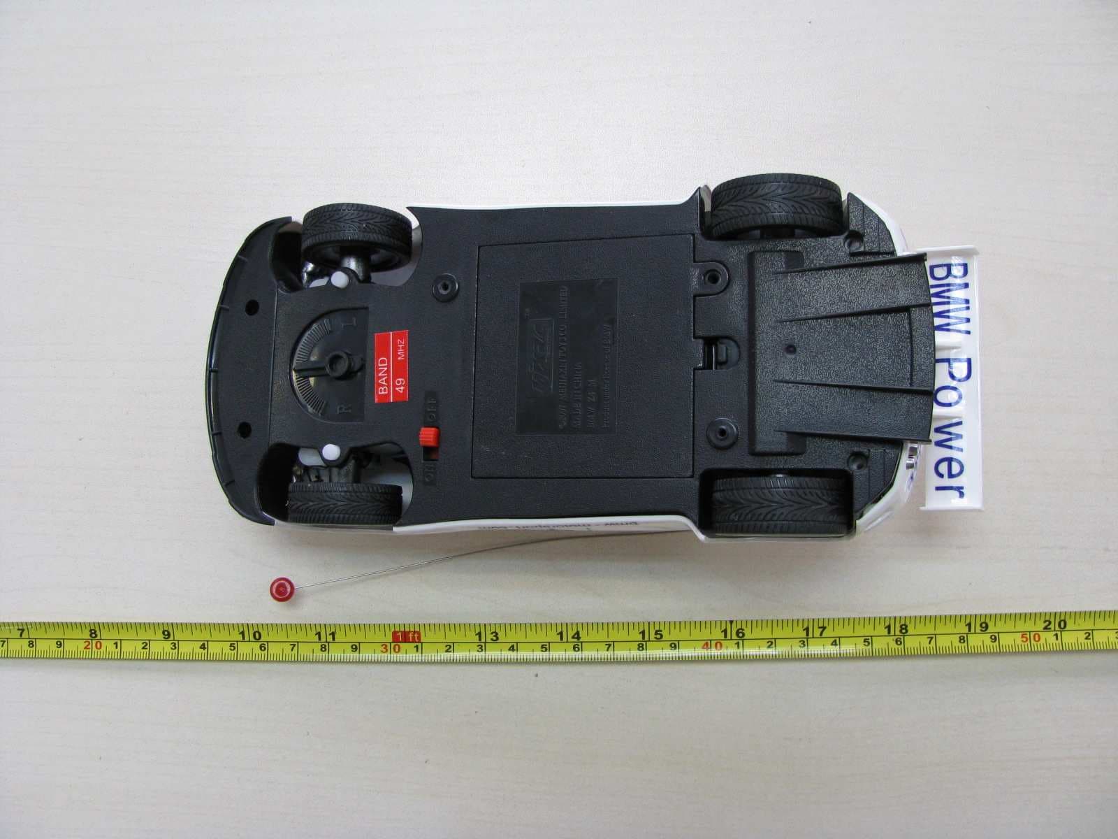
TRI8109R
Feb 04, 2008RC Car
Equipment Class
CRR - Superregenerative Receiver
TRI8109B
Feb 04, 2008RC Car
Equipment Class
DXX - Part 15 Low Power Communication Device Transmitter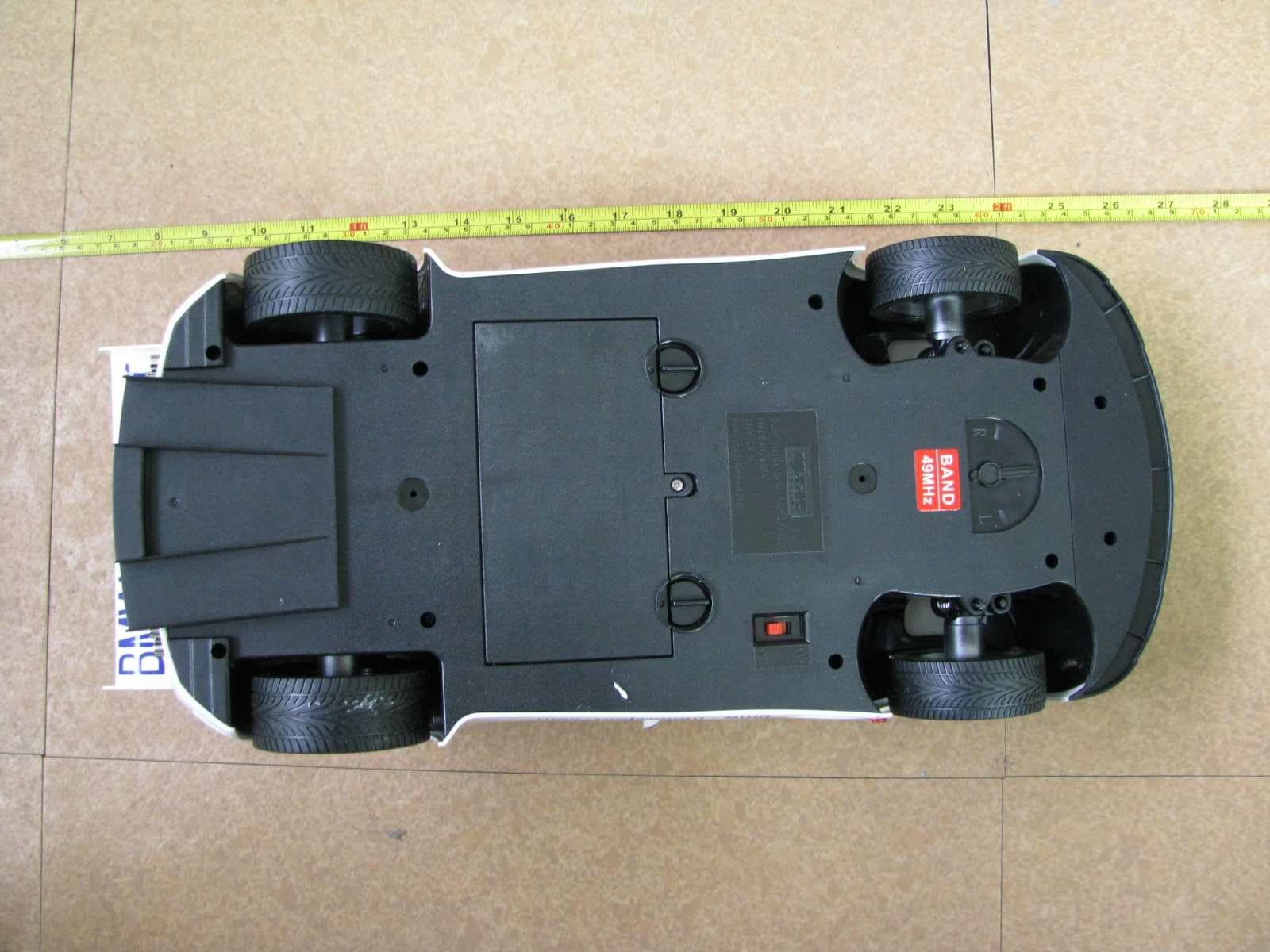
TRI8209R
Feb 04, 2008RC Car Receiver
Equipment Class
CRR - Superregenerative Receiver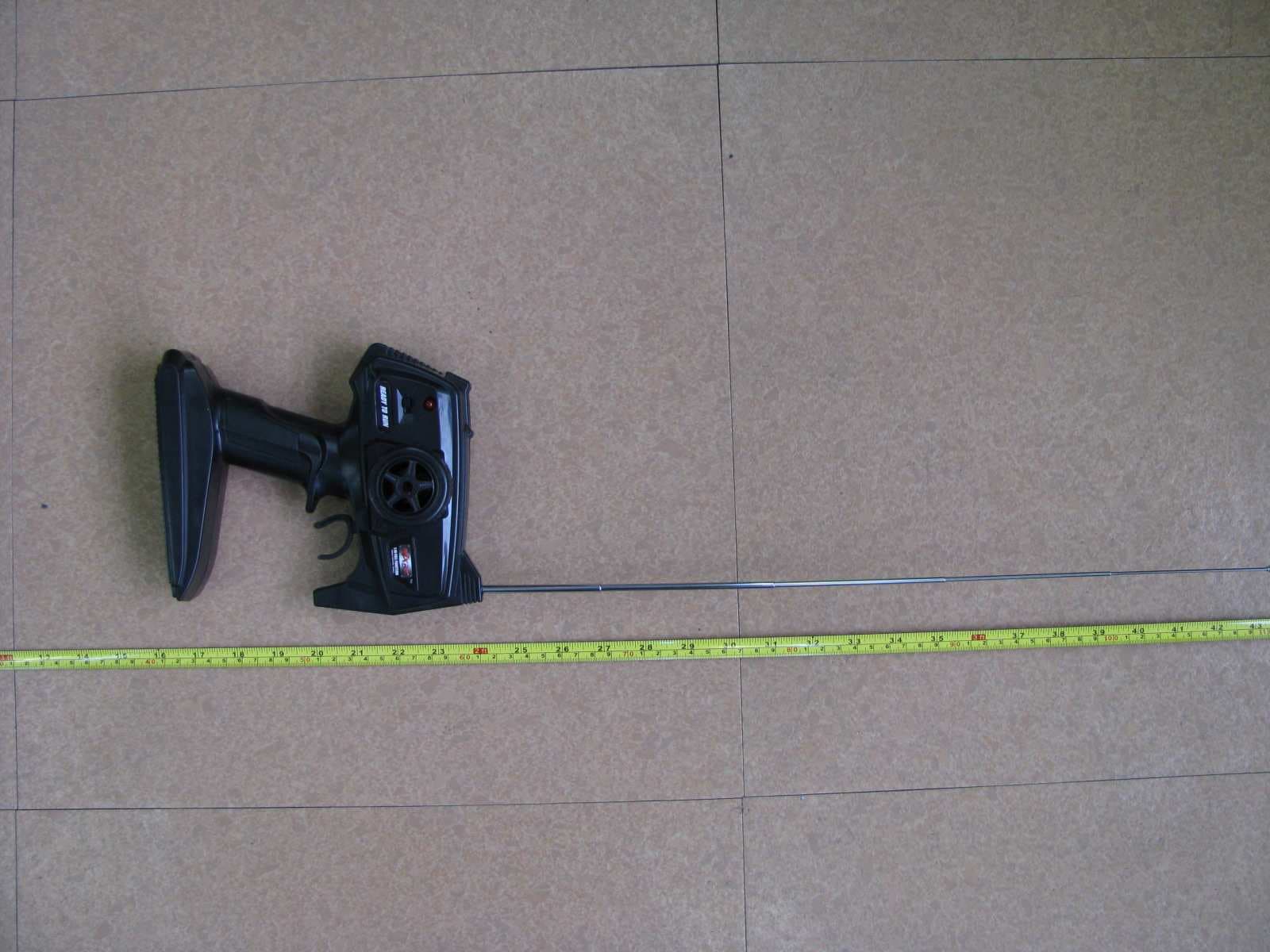
TRI8209A
Jan 31, 2008RC Car
Equipment Class
DXX - Part 15 Low Power Communication Device Transmitter
TRI8109A
Jan 30, 2008RC Car
Equipment Class
DXX - Part 15 Low Power Communication Device Transmitter