U2C-ATB-2015Tap Beacon
Outsite Networks, Inc.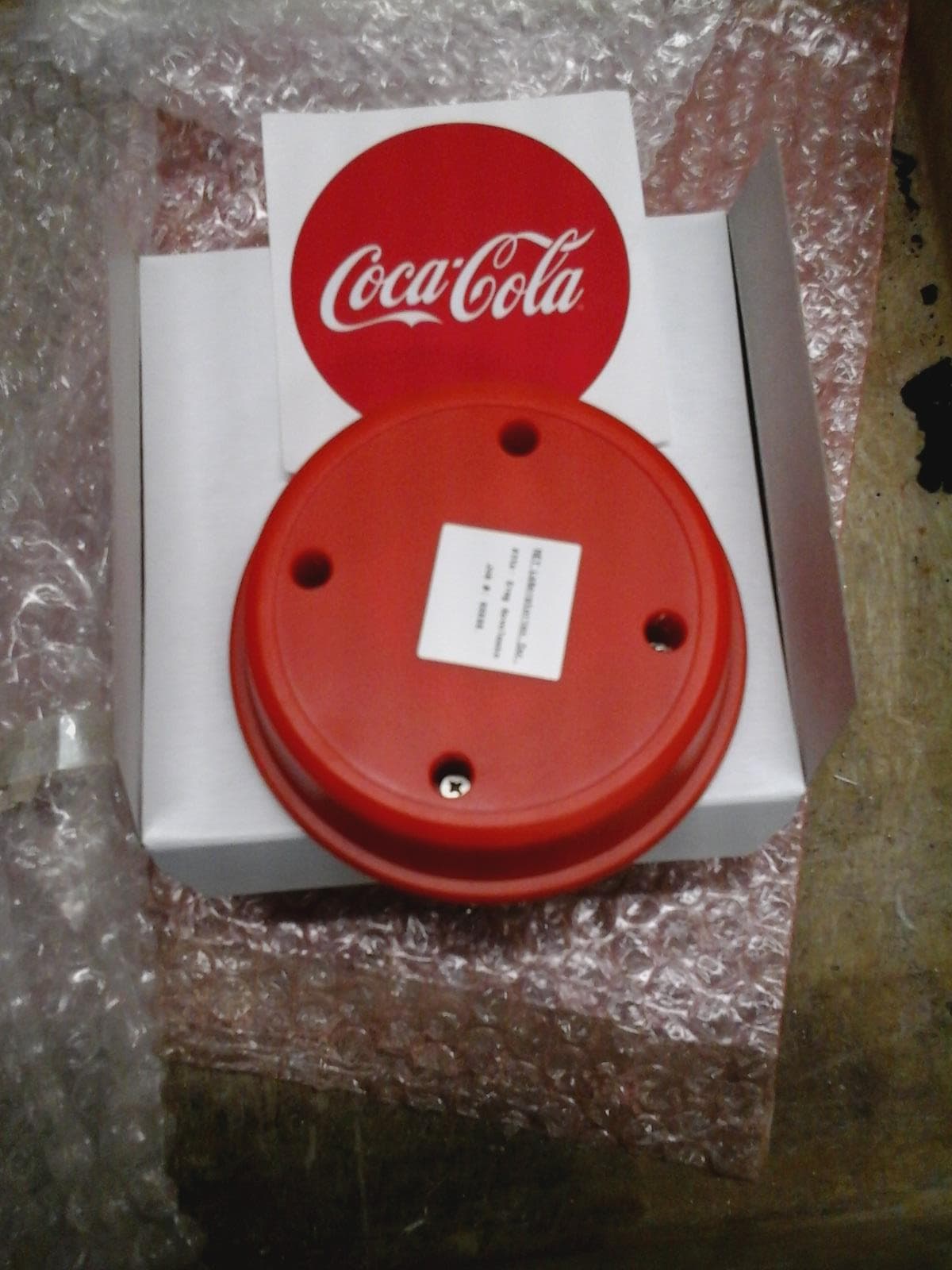
Click to zoom
Application Details
- Equipment Class
- DTS - Digital Transmission System
- Date of Grant
- Nov 10, 2015
- Application Purpose
- Original Equipment
- Date of Application
- Nov 10, 2015
- Equipment Note
- Tap Beacon
- Frequency Range
- 2402.00000000 - 2480.00000000
- Company
- Outsite Networks, Inc.
- Country
- United States
Documents & Files
Document Text
Text extracted from the exhibit documents filed with the FCC. Open a document above to read the original.
Users Manual
Tap-Beacon Quick Install Guide Outsite Network’s Tap-Beacon devices are dual platform beacons that transmit signals to enable mobile communication. Signals are transmitted via Bluetooth LE for Apple smartphones and NFC for Android smartphones. Tap-Beacon protocols follow predetermined specifications from both the Apple and Android operating systems. INSTALLATION & MOUNTING STEP 1 : Verify kit (brown box) has the correct site number and Tap-Beacon count. You will have one (1) Tap-Beacon per fueling station. Each Tap-Beacon will be packed individually in a small white box within the kit box. KEY FEATURES •Weather resistant ABS plastic 2 –part b eacon enclosure •Top and bottom pieces secured with fo ur (4) screws •AA batteries power ed •Preprogrammed •Companion Apps available for iOS and Android KIT CO NTENT •One (1) Tap-Beacon per fueling station •One (1) Tap-Beacon per white packaging box •2 AA B atteries pre -i n stalled •Tap-Beacons labeled by site and fueling station * Custom Stickers for Tap-Beacon provided separately STEP 2 : Check fueling station number and match with the Tap-Be acon sticker located on the top and bottom of th e enclosure. STEP 3: Identify which pump type you have for installation placement. You will install the Tap-Beacon in the location based on the pump type below. See illustrations below. Pump Type #1 Pump Type #2 Pump Type #3 Outsite Networks, Inc. Tap-Beacon Installation Guide 1.0 Note: This equipment has been tested and found to comply with the limits for a Class A digital device, pursuant to part 15 of th e FCC Rules. These limits are designed to provide reasonable protection against harmful interference when the equipment is operated in a commercial environment. This equipment generates, uses, and can radiate radio frequency energy and, if not i nstalled and used in accordance with the instruction manual, may cause harmful interference to radio communications. Operation of this equipment in a residential area is likely to cause harmful interference in which case the user will be required to correct interference at their expense. Modifications not expressly approved by the manufacturer could void the user's authority to operate the equipment under FCC rules. This device is compliant with UL60950/CSA 22.2 No. 60950-1 Second Edition. Listing# E113658. STEP 4 : Clean the surface where the Tap-Beacon will be mounted with rubbing alcohol. Remove protected layer from adhesive on the back of the Tap-Beacon. The pump number is also located on the back to prevent confusion. Ensure the mounting position is correct prior to positioning. Press fi rmly against the surface. The adhesive is 3M™ VHB™ Tape which has a very strong bond. THE TAP-BEACON CANNOT BE REPOSITIONED ONCE INSTALLED CERTIFICATIONS & PRODUCT WARNINGS Outsite Networks, Inc. Tap-Beacon Installation Guide 1.1 REMOVAL A specialized tool is required for Tap-Beacon removal. Removal instructions can be found at: http://multimedia.3m.com/mws/media/66962O/3mtm-vhbtm-tape-disassembly-tech-bulletin.pdf Part # #M 08978 Battery Warning: Only use batteries of correct type. Do not use rechargeable batteries or mix battery types. Do not expose unit to excessive heat or fire. Dispose of spent or damaged batteries according to manufacturer instructions and local laws. Safety Certification: Ou tsite Networks, Inc. 2551 Eltham Ave. Suite N Norfolk, VA 23513 Office 800-371-1118 Installation: Installation of Tap-Beacon device should be in compliance with the UL-87 standard for power operated dispensing devices for petroleum products. FCC United States: This Class B digital apparatus meets all requirements of the Canadian Interference Causing Equipment Regulations. Operation is subject to the following two conditions: (1) this device may not cause harmful interference, and (2) this device must accept any interference received, including interference that may cause undesired operation. Cet appareillage numérique de la classe [B] répond à toutes les exigences de l'interférence canadienne causant des règlements d'équipement. L'opération est sujette aux deux conditions suivantes: (1) ce dispositif peut ne pas causer l'interférence nocive, et (2) ce dispositif doit accepter n'importe quelle interférence reçue, y compris l'interférence qui peut causer l'opération peu désirée Canada IC: 6944A-ATB
Block Diagram
2.2 - NEOVENTUS DES. GRP. 13 All Points Beacon 4 (APB4) CONFIDENTIAL Outsite Networks, Inc 2551 Eltham Avenue, Ste. N Norfolk, VA 23513 Block Diagram https:\\www2.outsitenetworks.com/ 20-10-2015_10:11 NOTES Rev. Date Description Revision History 456321 REV SCALESHEET DWG NO 123654 B AA B C D C D of DRAWN BY SIZE TITLE PREPARED FOR:BY: C Neoventus Design Group, LLC 2350 Commonwealth Dr. Suite E Charlottesville, VA 22901 www.neoventus.com 32MHz XTAL Sheet 2 XTAL Holder CC2541 ANTENNA BLE Initial Release Sheet 2 Sheet 2 HEADER +3.0V-BAT 2015.March.262.0 2x AA Battery DEBUG DEBUG w/ Bypass Mode SWITCHING Sheet 3 Sheet 3 +VDD Depopulated debug LEDs This component may be a contigency or for developement only. 1. The symbol denotes components not (normally) inserted. Copyright (C) 2015 Outsite Networks, Inc. All rights reserved. Confidential and trade secret material of Outsite Networks, Inc. SERIAL HEADER Sheet 2 Sheet 2 DEBUG LED USART0 GPIO I2C I2C TPs Sheet 2 2015.March.272.1 ADC 2.2 GPIO REGULATOR 2015.June.9 Populated 32kHz xtal circuit NFC TAG STICKER OFF BOARD COMPONENTS ON BOARD COMPONENTS 2.4 GHz 115,2 Kbaud
ID Label/Location Info
FCC Label Design: Label location: Model: ATB FCC ID: U2C-ATB-2015 IC: 6944A-ATB Outsite Networks, Inc. 2.0” 1.0” Descr.: Tap Beacon Serial#: Part#: ATB01000 Bottom Top File: Tap Beacon Description and Label Page 2
Operational Description
Tap Beacon Functional Description The Tap Beacon is a non-connectable Bluetooth low energy (BLE) device in broadcasting mode. It transmits information that is stored internally. Because the non-connectable broadcasting does not activate any receiving capabilities, it achieves the lowest possible power consumption by simply waking up, transmit data and going back to sleep. The default wake up cycle is once per second but can be adjusted through special commands. All functionality is provided by the CC2541 single chip processor. The radio uses a chip antenna (2450AT42A100) The device is powered by two AA batteries, resulting in an expected life of over two years. No external connections exist. In addition to the BLE Beacon a passive NFC RFID chip (Mifare Ultralight) is mounted inside the device. There is no connection between RFID and BLE devices. File: Tap Beacon Description and Label Page 1
Parts List/Tune Up Info
Bill-of-Material Outsite Networks Inc. - All Points Beacon 4 (APB4) Assembly: Version: R202 Generated: Ma y 15, 2015 *** This BOM is RoHS compliant *** Items changed from previous revision (R201) *NOTE* Packaging specification fields (e.g. reel, tube, bulk pack ...) have been replaced by '-' in Mfg Part Numbe ITEMQTYRef-DesNEOVENTUS P/NVALUEDESCRIPTIONPACKAGEMANUFACTURER 1MFGR1 PART NUMBERMANUFACTURER 2 MFGR2 PART NUMBER 11R51112‐00021.00KRES, 0402, 1%, 1/16W, 1.00K402PANASONICERJ‐2RKF1001ROHMMCR01‐‐‐F1001 22R2,R101112‐00052.21KRES, 0402, 1%, 1/16W, 2.21K402PANASONICERJ‐2RKF2211ROHMMCR01‐‐‐F2211 31R11112‐006756.2KRES, 0402, 1%, 1/16W, 56.2K402PANASONICERJ‐2RKF5622ROHMMCR01‐‐‐F5622 45R6,R12,R13,R14,R151113‐00010, JUMPERRES, 0402, 5%, 1/16W, JUMPER, 0, THICK FILM402PANASONICERJ‐2GE0R00ROHMMCR01‐‐‐J000 52C1,C22104‐0002220PFCAP, CERAMIC, NPO, 0402, 220pF, 5%, 50V402MURATAGRM1555C1H221JA01TDKC1005C0G1H221J050BA 62C4,C62104‐001115PFCAP, CERAMIC, NPO, 0402, 15pF, 5%, 50V402AVX04025A150JAT‐AMURATAGRM1555C1H150JZ01 76C14,C15,C16,C17,C18,C192134 ‐00110.1UFCAP, CERAMIC, X7R, 0402, 0.1uF, 10%, 16V402MURATAGRM155R71C104KA88TDKC1005X7R1C104K 82C7,C82164‐00081.0UFCAP, CERAMIC, X5R, 0402, 1.0uF, 10%, 16V402TDKC1005X5R1C105KTAIYO YUDENEMK105BJ105KV‐F 92C11,C212167‐000610UFCAP, CERAMIC, X5R, 0603, 10uF, 20%, 6.3V603TAIYO YUDENJMK107BJ106MAAVX06036D106MAT‐A 101FB13101‐00020.25A BEADFERRITE BEAD, 0402, 0.25A, 1000 OHM402MURATABLM15HG102SN1D 111T13420‐00022450BM15A0002 TRANSFORMER, BALUN, 2400‐2500MHz, BAL IN/UNBAL OUT805JOHANSON TECHNOLOGIES2450BM15A0002 121ANT13900‐00012450AT42A100 ANTENNA, 2400 ‐ 2500 Mhz, ‐1 dBi typ. (XZ ‐V) GAIN, 9.5 dB R‐LOSSSMJOHANSON TECHNOLOGIES2450AT42A100 131Y24142‐001232.000MHZXTAL, 32.000 MHZ, 10ppm, 10pF, ‐40 to +85C, 2.0X1.6MM, No Pb2.0x1.6MM EPSONFA‐128 32.0000MF20X‐K 141U14421‐0001CC2541IC, WIRELESS BLUETOOTH LOW ENERGY, 8051 uP, 256kB FLASH, 8kB RAMQFN41 TICC2541F256RHAT 150‐5120‐0003GREENLED, GREEN, SM, 0805805CML7012X5 161Q15410‐0006FDV301NTRANSISTOR, N‐CHAN FET, 25V, 220mASOT‐23 FAIRCHILD SEMICONDUCTOR FDV301N 171Q25411‐0009DMP2100UTRANSISTOR, P‐CHAN FET, 20V, 3.4A, 0.075 RDSSOT‐23 DIODES INCDMP2100U‐7 181J26512‐0004SOCKET, BATT, 2 AA SOCKET, BATTERY HOLDER, 2 AA, IN SERIES, NICKEL, THTHKEYSTONE ELECTRONICS2462 191‐ PCB 2‐Layer, RoHS, Beacon 4 R02 201Y14140‐000632.768KHZXTAL, 32.768KHZ, 20PPM, 12.5pF, ‐40‐85C, 3.2X1.5MM, No Pb3.2x1.5MM NDKNX3215SA‐32.768K‐STD‐MUA‐8 212C9,C102104‐001618PFCAP, CERAMIC, NPO, 0402, 18pF, 5%, 50V402MURATAGRM1555C1H180JZ01AVX04025A180JAT ‐A Note: 1. The following reference designators are NOT INSERTED 1R91112‐000310.0KRES, 0402, 1%, 1/16W, 10.0K402PANASONICERJ‐2RKF1002ROHMMCR01‐‐‐F1002 2R3,R41112‐00052.21KRES, 0402, 1%, 1/16W, 2.21K402PANASONICERJ‐2RKF2211ROHMMCR01‐‐‐F2211 2R7,R81112‐0098174RES, 0402, 1%, 1/16W, 174, THICK FILM402VISHAYCRCW0402174RFKPANASONICERJ‐S02F1740 1R111113‐00010, JUMPERRES, 0402, 5%, 1/16W, JUMPER, 0, THICK FILM402PANASONICERJ‐2GE0R00ROHMMCR01‐‐‐J000 2C3,C52104‐001115PFCAP, CERAMIC, NPO, 0402, 15pF, 5%, 50V402AVX04025A150JAT‐AMURATAGRM1555C1H150JZ01 0‐2104‐001618PFCAP, CERAMIC, NPO, 0402, 18pF, 5%, 50V402MURATAGRM1555C1H180JZ01AVX04025A180JAT‐A 2C12,C132134‐00110.1UFCAP, CERAMIC, X7R, 0402, 0.1uF, 10%, 16V402MURATAGRM155R71C104KA88TDKC1005X7R1C104K 2C22,C232165‐00042.2UFCAP, CERAMIC, X5R, 0402, 2.2uF, 20%, 6.3V402TAIYO YUDENJMK105BJ225MVTDKC1005X5R0J225M050BC 1C202167‐000610UFCAP, CERAMIC, X5R, 0603, 10uF, 20%, 6.3V603TAIYO YUDENJMK107BJ106MAAVX06036D106MAT‐A 1L13153‐00042.2UHINDUCTOR, 2.2uH, 800mA, 25%, SM, 0805, RoHS805MURATALQM21PN2R2NGCD 1U24120‐0032TPS62730IC, SWITCH REG, BUCK, 3MHz, 2.1V, 100mASON6 TITPS62730DRY 0‐4140‐000632.768KHZXTAL, 32.768KHZ, 20PPM, 12.5pF, ‐40‐85C, 3.2X1.5MM, No Pb3.2x1.5MM NDKNX3215SA‐32.768K‐STD‐MUA‐8 1D15103‐0008SMAZ9V1DIODE, ZENER, 9.1V, +/‐5%, 1W, SMASMA MICRO COMMERCIALSMAZ9V1‐TP 2LD1,LD25120‐0003GREENLED, GREEN, SM, 0805805CML7012X5 1J16101‐0032VERT MALE, 5X2 CONN, SM, 5X2, 0.05IN, VERT, MALE, POST HGHT=0.120", FLSH GOLDSMSAMTECFTS‐105‐01‐F‐DV‐P 8MP1,MP2,MP3,MP4,MP5,MP6,MP7,MP89996‐0001SM 1.0MMMOD POINT, SM, 1.0mm (39 mil) SQUARE PADSM 4FID1,FID2,FID3,FID49997‐0001FID 1.05MMFIDUCIAL, SM, 1.05mm PAD, 1.8mm MASKSM 8TP1,TP2,TP3,TP4,TP5,TP6,TP7,TP89998‐0003SM 1.0MMTEST POINT, SM, 1.0mm (39 mil) PADSM 4MT1,MT2,MT3,MT49999‐00213.175MMMOUNT HOLE, NON‐PLATED, 3.175mm (125mil) HOLETH
RF Exposure Info
2.45 GHz AntennaP/N 2450AT42A100 Detail Specification: 01/25/2012 Page 1 of 3 General Specifications Part NumberInput Power Frequency RangeImpedance Peak GainOperating Temp. Average GainReel Quanity Return Loss Terminal Configuration BulkSuffix = S P/N T & RSuffix = E Suffix 100% Tin Suffix = None No. Function 1Feeding Point Mechanical Dimensions2NC Inmm L±± W±± T±± a±± Mounting Considerations Mount these devices with brown mark facing up. Units: mm Units:mm Johanson Technology, Inc. reserves the right to make design changes without notice. All sales are subject to Johanson Technology, Inc. terms and conditions. www.johansontechnology.com 4001 Calle Tecate • Camarillo, CA 93012 • TEL 805.389.1166 FAX 805.389.1821 2012 Johanson Technology, Inc. All Rights Reserved 2450AT42A100 2,000 -40 to +85°C 50 Ω 3 Watts max. 9.5 dB min. -1 dBi typ. (XZ-V) 0 dBi typ. (XZ-V) 2400 - 2500 Mhz Eg. 2450AT42A100(E or S) Eg. 2450AT42A100E Eg. 2450AT42A100S Termination Style Evaluation Board 0.20 *Line width should be designed to provide 50Ω impedance matching characteristics. Final monting on customer's PCB might need a shunt-series-shunt type antenna matching circuit Packaging Style 2450AT42A100-EB1SMA 0.500.30 0.1970.008 1.10 0.20 0.008 0.205.00 "High Frequency Ceramic Solutions" 0.0200.012 0.079 0.043 2.000.008 12 L W a T * 3.9 8.9 1.8 1.0 4.0 1.0 GND GND 50Ω Trace 2.45 GHz AntennaP/N 2450AT42A100 Detail Specification: 01/25/2012 Page 2 of 3 Typical Electrical Characteristics (T=25 o C) Test Board: Vias Return Loss *No Matching Circuit required Storage Conditions Johanson Technology, Inc. reserves the right to make design changes without notice. All sales are subject to Johanson Technology, Inc. terms and conditions. www.johansontechnology.com 4001 Calle Tecate • Camarillo, CA 93012 • TEL 805.389.1166 FAX 805.389.1821 2012 Johanson Technology, Inc. All Rights Reserved "High Frequency Ceramic Solutions" +5 to +35°C, Humidity: 45- 75%RH, 18 mos. Max Antenna* No Ground Ground 18mm 18mm 30mm 9.6mm 50Ω Feed Line ) ) ) ) ) ) ) ) ) 39.6mm 2.45 GHz AntennaP/N 2450AT42A100 Detail Specification: 01/25/2012Page 2 of 3 Typical Radiation Patterns Johanson Technology, Inc. reserves the right to make design changes without notice. All sales are subject to Johanson Technology, Inc. terms and conditions. www.johansontechnology.com 4001 Calle Tecate • Camarillo, CA 93012 • TEL 805.389.1166 FAX 805.389.1821 2012 Johanson Technology, Inc. All Rights Reserved "High Frequency Ceramic Solutions" ) ) ) ) ) ) ) ) ) XY-V/XY-H 180° 270° 0° 90° X Z Y XY-cut scanning direction XY cut @2.45GHz Vertical Horizontal XZ-V/XZ-H YZ-V/YZ-H 180° 270° 0° 90° X Z Y XZ-cut scanning direction 180° 270° 0° 90° X Z Y YZ-cut scanning direction XZ cut @2.45GHz Vertical Horizontal YZ cut @2.45GHz Vertical Horizontal
RF Exposure Info
§ 15.247(i) Maximum Permissible Exposure RF Exposure Requirements: §1.1307(b)(1) and §1.1307(b)(2): Systems operating under the provisions of this section shall be operated in a manner that ensures that the public is not exposed to radio frequency energy levels in excess of the Commission’s guidelines. RF Radiation Exposure Limit: §1.1310: As specified in this section, the Maximum Permissible Exposure (MPE) Limit shall be used to evaluate the environmental impact of human exposure to radiofrequency (RF) radiation as specified in Sec. 1.1307(b), except in the case of portable devices which shall be evaluated according to the provisions of Sec. 2.1093 of this chapter. MPE Limit Calculation: EUT’s operating frequencies @ 2400-2483.5 MHz; highest conducted power = 2.89dBm (peak) therefore, Limit for Uncontrolled exposure: 1 mW/cm 2 or 10 W/m 2 EUT maximum antenna gain = 0 dBi. Equation from page 18 of OET 65, Edition 97-01 S = PG / 4R 2 or R = √PG / 4S where, S = Power Density (1 mW/cm 2 ) P = Power Input to antenna (1.945mW) G = Antenna Gain (1 numeric) S = (1.945*1/ 4*3.14*20 2 ) = 0.0004 mW/cm 2
Schematics
2.2 - NEOVENTUS DES. GRP. 13 All Points Beacon 4 (APB4) CONFIDENTIAL Outsite Networks, Inc 2551 Eltham Avenue, Ste. N Norfolk, VA 23513 Block Diagram https:\\www2.outsitenetworks.com/ 20-10-2015_10:11 NOTES Rev. Date Description Revision History 456321 REV SCALESHEET DWG NO 123654 B AA B C D C D of DRAWN BY SIZE TITLE PREPARED FOR:BY: C Neoventus Design Group, LLC 2350 Commonwealth Dr. Suite E Charlottesville, VA 22901 www.neoventus.com 32MHz XTAL Sheet 2 XTAL Holder CC2541 ANTENNA BLE Initial Release Sheet 2 Sheet 2 HEADER +3.0V-BAT 2015.March.262.0 2x AA Battery DEBUG DEBUG w/ Bypass Mode SWITCHING Sheet 3 Sheet 3 +VDD Depopulated debug LEDs This component may be a contigency or for developement only. 1. The symbol denotes components not (normally) inserted. Copyright (C) 2015 Outsite Networks, Inc. All rights reserved. Confidential and trade secret material of Outsite Networks, Inc. SERIAL HEADER Sheet 2 Sheet 2 DEBUG LED USART0 GPIO I2C I2C TPs Sheet 2 2015.March.272.1 ADC 2.2 GPIO REGULATOR 2015.June.9 Populated 32kHz xtal circuit NFC TAG STICKER OFF BOARD COMPONENTS ON BOARD COMPONENTS 2.4 GHz 115,2 Kbaud 2.2 - NEOVENTUS DES. GRP. 2 3 20-10-2015_10:11 All Points Beacon 4 (APB4) CONFIDENTIAL Bluetooth 4 5 6 3 2 1 REV SCALE SHEET DWG NO 1 2 3 6 5 4 B A A B C D C D of DRAWN BY SIZE TITLE C MP1 SM 1.0MM SM MP2 SM 1.0MM SM +VDD 2.21K 1% 0402 R2 +VDD +VDD-RF X7R 10% 16V 0402 0.1UF C12 X7R 10% 16V 0402 0.1UF C13 R6 5% 0, JUMPER 0402 2450BM15A0002 T1 3 5 1 2 6 4 ANT1 2450AT42A100 SM 1 +VDD-RF FB1 0.25A BEAD 0402 1000 OHM C14 0.1UF 0402 16V 10% X7R C15 0.1UF 0402 16V 10% X7R C16 0.1UF 0402 16V 10% X7R C17 0.1UF 0402 16V 10% X7R 10UF 0603 6.3V 20% X5R C11 220pF 5% 0402 50V NPO C2 0.1UF C18 X7R 10% 16V 0402 +VDD-RF C19 0.1UF 0402 16V 10% X7R C8 1.0UF 0402 16V 10% X5R Y2 32.000MHZ 2.0x1.6MM 4 2 3 1 CASE1 CASE2 R3 2.21K 0402 1% 5% 50V 0402 15PF C3 NPO 1% 0402 2.21K R4 0402 15PF C4 NPO 5% 50V NPO C5 15PF 0402 50V 5% C1 220PF 0402 50V 5% NPO SM SM 1.0MM MP3 SM SM 1.0MM MP4 C6 15PF 0402 50V 5% NPO +VDD-RF X5R 10% 16V 0402 1.0UF C7 R1 56.2K 0402 1% 20mA 62.5mW LD1 GREEN 0805 2.1VF 20mA 62.5mW LD2 GREEN 0805 2.1VF R7 174 0402 1/16W 1% R8 174 0402 1/16W 1% +VDD-EXT-DBG Y1 32.768KHZ 3.2x1.5MM C9 18PF 0402 50V 5% NPO C10 18PF 0402 50V 5% NPO U1 CC2541 QFN41 8 6 41 24 31 22 23 19 18 17 16 15 14 13 12 36 10 35 34 33 32 11 39 9 7 5 38 37 20 27 1 4 2 3 40 28 30 25 26 29 21 AVDD_5 AVDD_4 RF_N RF_P RBIAS AVDD_1 DCOUPL SDA SCL NC4 GND AVDD_2 RESET_N P1[7] P1[6] P1[5] P1[3] P1[1] DVDD_1 P1[0] P2[4]/XOSC32K_Q1 P2[3]/XOSC32K_Q2 P2[2] P2[1] DVDD_2 P2[0] P0[7] P0[6] P0[5] P0[4] P0[3] P0[2] P0[1] P0[0] XOSC_Q2 XOSC_Q1 AVDD_6 AVDD_3 PAD P1[4] P1[2] VERT MALE, 5X2 SM J1 1 3 5 7 9 2 4 8 6 10 +VDD TP1 SM 1.0MM SM TP2 SM 1.0MM SM TP3 SM 1.0MM SM TP4 SM 1.0MM SM TP5 SM 1.0MM SM SM SM 1.0MM MP5 SM SM 1.0MM MP6 SM SM 1.0MM MP7 SM SM 1.0MM MP8 <3-B4> <3-B6> <3-C3> +VDD-RF 0402 0, JUMPER 5% R14 +3.0V-BAT +VDD-RF BLE-DEBUG-DATA BLE-DEBUG-DATA BLE-RF-P BLE-RF-N BLE-SCL BLE-SDA BLE-DEBUG-CLK BLE-DEBUG-CLK BLE-DEBUG-LED BLE-DEBUG-LED BLE-USART0-CTS BLE-USART0-CTS BLE-USART0-RTS BLE-USART0-RTS BLE-USART0-RX BLE-USART0-RX BLE-USART0-TX BLE-USART0-TX BLE-DBG-RST-N BLE-DBG-RST-N MEASURE-BATT BATT-LEVEL SWITCHER-ON SOC Filters and Decoupling BLE Serial Test Points Design Note: Reset min pulse width = 1us i i Stitching Capacitors Do Not Insert i For Contingency Purposes Design Note: BLE Debug Header Design Note: P1_0 & P1_1 have 20mA drive capability LEDs i Remove battery when using Design Note: supply from debugger +3.0V-BAT TH 3.175MM MT1 TH 3.175MM MT2 +3.0V-IN TH 3.175MM MT3 TH 3.175MM MT4 800mW 20V 3.4A SOT-23 DMP2100U Q2 X5R 20% 6.3V 0603 10UF C20 SM FID 1.05MM FID1 SM FID 1.05MM FID2 SM FID 1.05MM FID3 SM FID 1.05MM FID4 X5R 20% 6.3V 0603 10UF C21 1W 9.1V SMA SMAZ9V1 D1 I TH SOCKET, BATT, 2 AA J2 N1 P1 2.2 - NEOVENTUS DES. GRP. 3 3 20-10-2015_10:11 All Points Beacon 4 (APB4) CONFIDENTIAL POWER 4 5 6 3 2 1 REV SCALE SHEET DWG NO 1 2 3 6 5 4 B A A B C D C D of DRAWN BY SIZE TITLE C <2-C5> 1% 1.00K R5 0402 R10 2.21K 0402 1% +3.0V-BAT <2-C5> 5% R12 0, JUMPER 0402 Q1 FDV301N SOT-23 220mA 25V 5% R11 0, JUMPER 0402 SM SM 1.0MM TP7 10.0K 1% R9 0402 <2-C5> L1 2.2UH 0805 800mA +VDD +3.0V-BAT C22 2.2UF 0402 6.3V 20% X5R C23 2.2UF 0402 6.3V 20% X5R U2 TPS62730 SON6 1 6 2 4 3 5 ON/BYP VIN GND SW VOUT STAT SM SM 1.0MM TP6 5% R13 0, JUMPER 0402 0402 0, JUMPER R15 5% TP8 SM 1.0MM SM MEASURE-BATT BATT-LEVEL TPS62730-STAT TPS62730-SW SWITCHER-ON Fiducials Battery Monitor Battery Holder changes from DC/DC to bypass. Mechanical i Design Note: When in DC/DC mode, nominal output voltage is 2.10V 2.20V, the regulator automatically i Design Note: When Batt Voltage drops below Switching Regulator
Test Setup Photos
Photograph 1. Radiated Spurious Emissions, Test Setup (1) Photograph 2. Radiated Spurious Emissions, Test Setup (2)
Contact Information
Applicant
Chuck Mooring(VP of Engineering)
Test Firm
EUROFINS ELECTRICAL AND ELECTRONIC TESTING NA, INCGreg Kovolenko
Technical Specifications
| # | Rule Parts | Frequency Range | Power Output |
|---|---|---|---|
| 1 | 15C | 2.40 GHz - 2.48 GHz | 1.90 mW |
Other Applications from Outsite Networks, Inc.
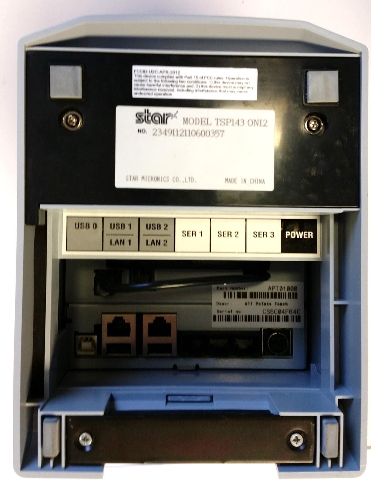
U2C-APT-2014
Jul 30, 2014AllPoints Touch Printer (APT)
Equipment Class
DXX - Part 15 Low Power Communication Device Transmitter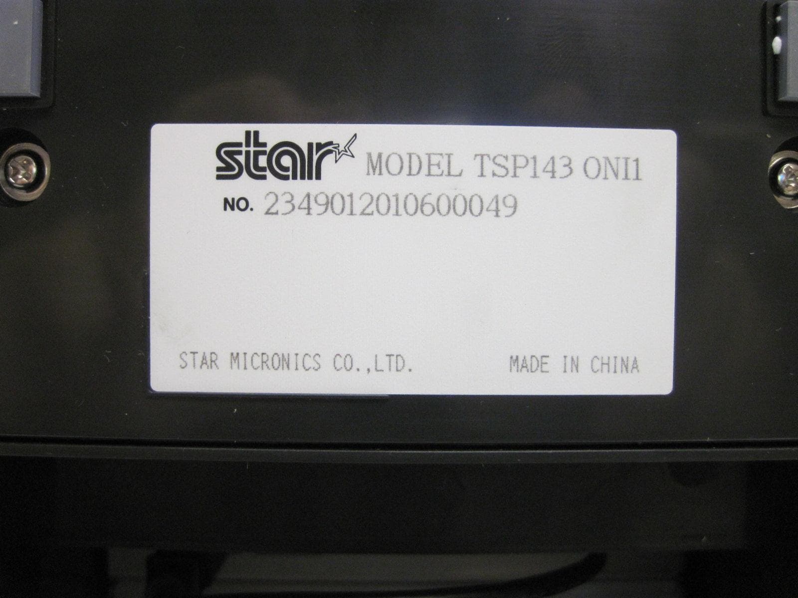
U2C-APX-2012
Dec 10, 2012All Points Printer
Equipment Class
DXX - Part 15 Low Power Communication Device Transmitter
U2C-AIO-2011
Jan 17, 2012All In One Printer
Equipment Class
DXX - Part 15 Low Power Communication Device Transmitter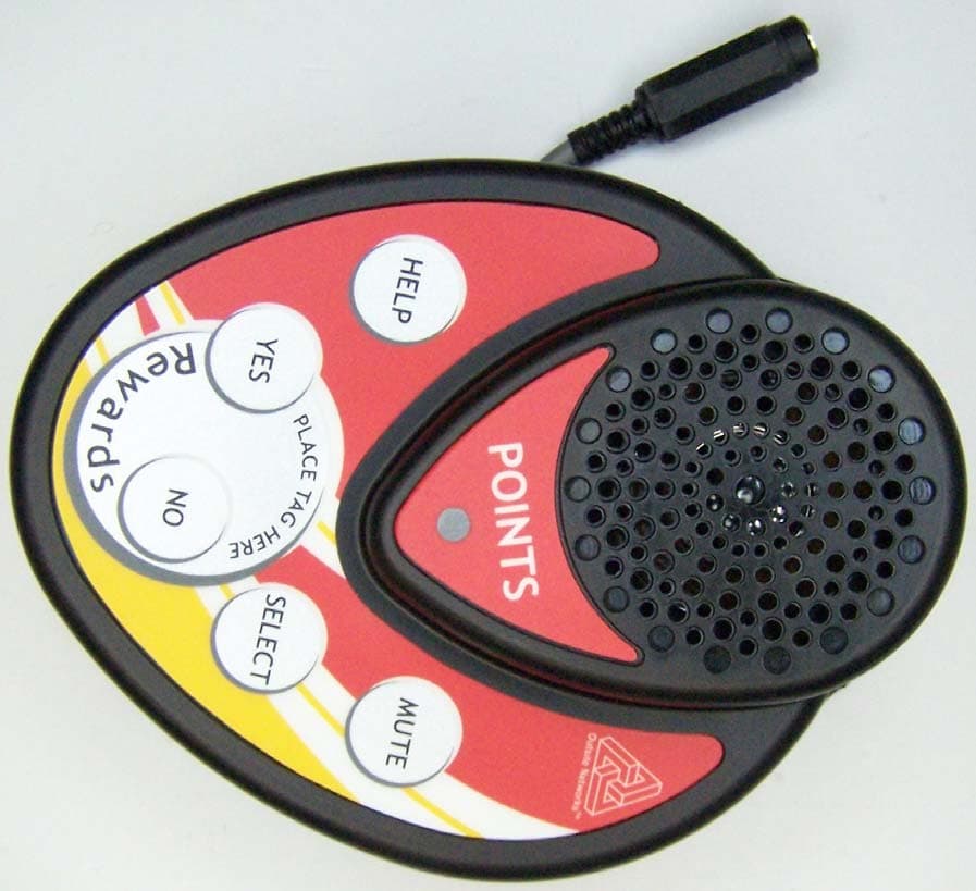
U2C-FMPWR-2-3
Mar 07, 20072.4GHz TOUCHPOINT
Equipment Class
DTS - Digital Transmission System