UDV-0912142009007Quad-band GSM/GPRS module
Shanghai Simcom Ltd.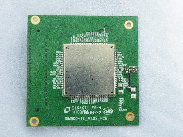
Click to zoom
Application Details
- Equipment Class
- PCB - PCS Licensed Transmitter
- Date of Grant
- Feb 22, 2010
- Application Purpose
- Original Equipment
- Date of Application
- Feb 22, 2010
- Equipment Note
- Quad-band GSM/GPRS module
- Frequency Range
- 1850.20000000 - 1909.80000000
- Company
- Shanghai Simcom Ltd.
- Country
- China
Documents & Files
Document Text
Text extracted from the exhibit documents filed with the FCC. Open a document above to read the original.
Users Manual
SMT Module RF Reference Design Guide AN_ SMT Module RF Reference Design Guide _V1.01 Document Title: SMT Module RF Reference Design Guide Version: 1.01 Date: 2010-1-27 Status: Release Document Control ID: AN_SMT Module RF Reference Design Guide_V1.01 General Notes SIMCOM offers this information as a service to its users, to support application and engineering efforts that use the products designed by SIMCOM. The information provided is based upon requirements specifically provided to SIMCOM by the users. SIMCOM has not undertaken any independent search for additional relevant information, including any information that may be in the user’s possession. Furthermore, system validation of this product designed by SIMCOM within a larger electronic system remains the responsibility of the user or the user’s system integrator. All specifications supplied herein are subject to change . Copyright This document contains proprietary technical information which is the property of SIMCOM Limited., copying of this document and giving it to others and the using or communication of the contents thereof, are forbidden without express authority. Offenders are liable to the payment of damages. All rights reserved in the event of grant of a patent or the registration of a utility model or design. All specification supplied herein are subject to change without notice at any time. Copyright © Shanghai SIMCOM Wireless Solutions Ltd. 2010 SMT Module RF Reference Design Guide SMT Module RF Reference Design Guide 1 SMT Module RF Reference Design Guide 1 Introduction....................................................................................................................................2 2 Circuit design .................................................................................................................................2 2.1 Power supply circuit design ................................................................................................2 2.2 Antenna matching circuit design .........................................................................................3 3 Consideration in components placement........................................................................................4 4 Stacking up of multi-layers PCB....................................................................................................5 Stack-up of two-layers PCB ......................................................................................................5 Stack-up of four-layers PCB .....................................................................................................6 Stack-up of six-layers PCB .......................................................................................................6 Stack-up of eight-layers PCB ....................................................................................................7 5 Impedance control of RF trace .......................................................................................................7 6 Consideration in PCB layout........................................................................................................10 Appendix......................................................................................................................................... 11 Two-layers PCB ...................................................................................................................... 11 Four-layers PCB......................................................................................................................12 Six-layers PCB ........................................................................................................................13 Eight-layers PCB.....................................................................................................................16 Version History Data Version Description of change Author 2010-1-20 01.01 Origin Ye Haibing, Wang Guoqiang SMT Module RF Reference Design Guide SMT Module RF Reference Design Guide 2 1 Introduction This document describes the important points about RF that should be taken into account in client’s application design. As SMT module can be integrated with a wide range of applications, the application notes are described in detail. SMT module is a new and key product which is provided by SIMCom inc. This type module become very popular soon after it is released for its easy integration, good reliability. But bad RF design will lead to serious RF problems. In order to improve the RF performance, this document is formed to give the customer some design guides in RF design of SMT type module integration. Based on such considerations, at the later section, this document will describe some key issues that should be paid more attention to. NOTE: this document can apply for all SMT Modules, for example, SIM300D, SIM340D, SIM300W, SIM340W, SIM500W, SIM540W, SIM700D, SIM900, SIM900A, SIM900D, and so on. SIM900 is selected as a demonstration in the last sections. 2 Circuit design When the customer begins to integrate the SMT type module into their product, the first thing to be considered is the circuit design. In this section, we will focus on the circuit design which is related to the RF performance. This section is divided into two sub-parts, the first is the power supply circuit design; the second is the antenna matching circuit design. 2.1 Power supply circuit design Because the SMT module is a high power consuming communication system, and the maximum working power will up to 2watt in worst case, so, this will form a large voltage drop at the module’s power supply port. To make the SMT module have a stabilized working condition, we recommended a large tantalum capacitor (100uF or more capacity is recommended) shunted to the module’s power supply port. To get better noise decoupling performance, some additional small ceramic capacitors can be added combined with the large capacitor. If the SMT module is power…
Text truncated - open the document above for the full version.
Users Manual
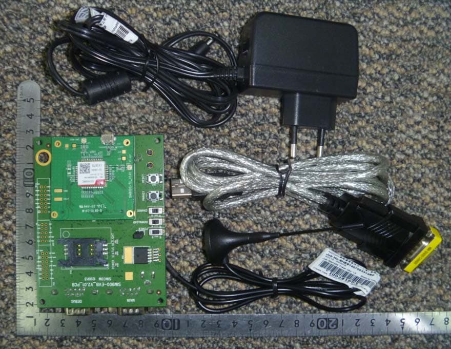
Development Kit Manual SIM900-EVB_UGD_V1.01 SIM900 EVB User Guide SIM900-EVB_UGD_V1.01 2 08.12.2009 Document Title: SIM900 EVB User Guide Ve r s i o n : 1.01 Date: 2009-12-8 Status: Release Document Control ID: SIM900-EVB_UGD_V1.01 General Notes Simcom offers this information as a service to its customers, to support application and engineering efforts that use the products designed by Simcom. The information provided is based upon requirements specifically provided to Simcom by the customers. Simcom has not undertaken any independent search for additional relevant information, including any information that may be in the customer’s possession. Furthermore, system validation of this product designed by Simcom within a larger electronic system remains the responsibility of the customer or the customer’s system integrator. All specifications supplied herein are subject to change. Copyright This document contains proprietary technical information which is the property of SIMCOM Limited., copying of this document and giving it to others and the using or communication of the contents thereof, are forbidden without express authority. Offenders are liable to the payment of damages. All rights reserved in the event of grant of a patent or the registration of a utility model or design. All specification supplied herein are subject to change without notice at any time. Copyright © Shanghai SIMCom Wireless Solutions Ltd. 2009 SIM900 EVB User Guide SIM900-EVB_UGD_V1.01 3 08.12.2009 Contents Contents ............................................................................................................................................3 Version History .................................................................................................................................3 1. SIM900 EVB.................................................................................................................................5 2. EVB accessory ..............................................................................................................................7 3. Accessory Interface .......................................................................................................................8 3.1 Power Interface ...................................................................................................................8 3.2 Audio Interface....................................................................................................................9 3.3 SIM card interface.............................................................................................................10 3.4 Antenna Interface .............................................................................................................. 11 3.5 RS232 Interface.................................................................................................................12 3.6 Operating Status LED .......................................................................................................13 4. Test Interface ...............................................................................................................................14 4.1 J103 ...................................................................................................................................14 4.2 J201 ...................................................................................................................................15 4.3 J104 ...................................................................................................................................16 5. EVB and accessory equipment....................................................................................................18 6. Illustration: ..................................................................................................................................19 6.1 Running:............................................................................................................................19 6.2 Connecting Net and calling ...............................................................................................19 6.3 Downloading .....................................................................................................................19 6.4 Turns off ............................................................................................................................19 Figure Index FIGURE 1: EVB TOP VIEW ................................................................................................................... 5 FIGURE 2: EVB BOTTOM VIEW.......................................................................................................... 6 FIGURE 3: EVB ACCESSORY............................................................................................................... 7 FIGURE 4: POWER INTERFACE .......................................................................................................... 8 FIGURE 5: AUDIO INTERFACE ........................................................................................................... 9 FIGURE 6: SIM CARD INTERFACE ...................................................................................................10 FIGURE 7: ANTENNA INTERFACE ................................................................................................... 11 FIGURE 8: SERIAL PORTS.................................................................................................................. 12 FIGURE 9: STATUSLED ...................................................................................................................... 13 FIGURE 10: TEST INTERFACE OVERVIEW..................................................................................... 14 FIGURE 11: J103 INTERFACE............................................................................................................. 14 FIGURE 12: J201 INTERFACE .......................…
Text truncated - open the document above for the full version.
Block Diagram
Block Diagram
Block Diagram
SIM900 LAYOUT Files including 6layers 1. Layer 1 2. Layer 2 3. Layer 3 4. Layer4 5. Layer 5 6. Layer 6
Cover Letter(s)
Shanghai Simcom Ltd. Shanghai Simcom Ltd. SIM Technology Building, No.633 Jinzhong Road, Changning District , Shanghai, P.R.China(Postalcode 200335) MET Laboratories, Inc. 914 West Patapsco Avenue Baltimore, MD 21230 RE: LETTER OF AGENT AUTHORIZATION To Whom It May Concern: We, the undersigned, hereby authorize (Jack Wu at SGS-CSTC Standards Technical Services (Shanghai) Co., Ltd.) to act on our behalf in all matters relating to application for equipment authorization, including the signing of all documents relating to these matters. We also hereby certify that no party to the application authorized hereunder is subject to the denial of benefits, including FCC benefits, pursuant to Section 5301 of the Anti-Drug Abuse Act of 1988, 21 U.S.C.853(a). This agreement expires one year from the current date. Sincerely, Tel : 021-32523134 By : Yongsheng Li By : at Shanghai Date : 2010.01.20
Cover Letter(s)
1 Shanghai Simcom Ltd. Long Term Confidentiality Request Letter To Whom It May Concern: This letter serves as an official request for confidentiality under sections 0.457 and 0.459 of CFR 47. We have requested that the SIM900_BOM are required to be submitted with this application be permanently withheld from public review. The above documents are company proprietary information that could never get into the possession of your competition). Please contact me if there is any information you may need. Sincerely, Tel : 021-32523134 By : Yongsheng Li By : (Signature) (Printed) Date : 2010.01.20
Cover Letter(s)
Shanghai Simcom Ltd. Licensed Modular Approval Requirements: 1 The final device is designed for mobile or fixed operation (Portable is not permitted – Reference TCB Exclusion List (17 July 2002) II (g)). [Shanghai Simcom Ltd]: The final device is designed for M2M applications. 2 The maximum antenna gain to allow compliance with RF exposure requirements is listed on the Grant of Certification for this device. [Shanghai Simcom Ltd]: 7.3 dBi for the 850 MHz band and 12.7 dBi for the 1900 MHz band. 3 The licensed module must have a FCC ID label on the device itself. That FCC ID label must be visible through a window on the final device or it must be visible when an access panel, door or cover is easily removed. If not, a second label must be placed on the outside of the final device that contains the following text: Contains “FCC ID: XXXXX” [Shanghai Simcom Ltd]:The label include printed FCC ID:UDV-0912142009007 would be placed on the final device. 4 The Grant should include the following words in the device description or grant notes: “modular transmitter” or “transmitter module”. [Shanghai Simcom Ltd]:Transmitter module is OK.
Cover Letter(s)
RT for FCC – 1 st Communication 1. Is the 1 dBi antenna listed in this filing the only antenna that will ever be used with the module? Yes. 2. The dc voltages applied to and dc currents into the several elements of the final radio frequency amplifying device for normal operation over the power ranges has not been provided as required by CFR47 2.1033(c)(8). Please provide these values. 3. It does not appear that a Tune-up procedure has been provided as required by CFR47 2.1033(c)(9). For comment 2 and 3,could you please explain it clearly ? and we can follow your way. 4. The part 22-24 test report lists the 99% bandwidth. However, the specific FCC rule parts ask for the 26 dB bandwidth. The 99% and 26 dB bandwidth are not the same. Please provide the 26 dB bandwidth and update test report. Updated as attached “SHEMO09120140805 22 24 report_v2” 5. The modular approval cover letter requirements are wrong. These requirements are for un-licensed transmitters. The current filings are for licensed bands. There are separate requirements (less stringent) for licensed transmitters. For this issue,could you please inform us whether we need not to fill the modular approval cover letter when we approval this licensed bands? If you require us fill the cover letter,what item need to fill? Because the client filled the cover letter following the rule of project before. 6. Please clarify if the module is only for vehicular use. The module is not for vehicular use. RT for FCC – 2 nd Communication #2 – the dc voltages and currents into and out of the final amplifier stages of the radio. Basically, provide a schematic or block diagram with the voltage levels and currents to and from the amplifiers or write a paragraph or two stating the values. PA USE VBAT as power supply directly #3 – A tune up procedure is a procedure used at the factory to make sure the power levels of the radio are within tolerances. In other words, how does the manufacturer make sure that the power levels are within tolerances? Updated as attached “SIM900_Ture-up procedure.pdf” #5 – Incorrect Modular approval letter was submitted. Updated as attached “Modular Approval Letter” RT for FCC – 3 rd Communication Item #2 in the licensed modular approval requirements is incorrect. The maximum antenna gain to allow compliance with RF exposure requirements are 7.3 dBi for the 850 GSM band and 18.7 dBi in the 1900 PCS bands. Please update the document with these values. The attched is updated RT IC – 1 st Communication 1. Please confirm that the measured Level specified in the receiver spurs tables (IC test report) include cable corrections and antenna correction factors. Updated as attached” SHEMO09120140807 ic_fcc report_v2” 2. The IC label is incorrect. The proper label should state “IC: xxx” and not “IC ID: xxx”. Updated as attached “SIM900 Label” 3. Please correct the Industry Canada package, Appendix B, with the values I have listed on this check sheet. Updated “TCBJ FORM-9 IC 7-17-09 - Industry Canada Package_0203” 4. The 99% bandwidth has been measured incorrectly. The resolution bandwidth should be set to 1% of the span as is possible without being below 1%. Please refer to section 4.6.1 of RSS Gen. Please update test report. Updated as attached” SHEMO09120140807 ic_fcc report_v2” 5. The RF evaluation should be marked for General Public Use. Additionally, the standard used for evaluation is incorrect. Updated “TCBJ FORM-9 IC 7-17-09 - Industry Canada Package_0203” 6. Please confirm that an Electronic serial number is assigned to each unit which uniquely identifies a cellular mobile station to any cellular system. Please refer to section 3.2 of RSS 132. Yes.Each unit have an Electronic serial number. RT IC – 2 nd Communication #4 – The 99 % bandwidth measurement is still incorrect. You have used a span of 1.5 MHz and therefore the RBW should be at least 15 kHz. If 15 kHz is not an option on the spectrum analyzer then the next higher setting should be used. Updated as attached “SHEMO09120140807 ic_fcc report_v3” and IC test report cover sheet_page 3 “TCBJ FORM-9 IC 7-17-09 - Industry Canada Package_0208_page3”
External Photos
SGS-CSTC Standards Technical Services ( (( (Shanghai) )) ) Co., Ltd. APPENDIX 1 PHOTOGRAPHS OF EUT SGS-CSTC Standards Technical Services ( (( (Shanghai) )) ) Co., Ltd. Front View of EUT Back View of EUT
Internal Photos
SGS-CSTC Standards Technical Services( (( (Shanghai) )) ) Co., Ltd. APPENDIX 2 PHOTOGRAPHS OF EUT SGS-CSTC Standards Technical Services( (( (Shanghai) )) ) Co., Ltd. Internal of EUT-1 Internal of EUT-2
Operational Description
General Technical Description Model: SIM900 Date: 2010-01-20 Brand: SIMCOM 1. Scope This document shows and provides the more detail information about the platform we used. The basic description for the Baseband and RF section are also included. SIM900 designed by SIMCOM is a quad band module which support GSM/GPRS. The baseband circuit is based on STE and RF circuit is based on RFMD. It works at quad bands, GSM850, EGSM900, DCS1800, and PCS1900 band. CPU clock is based on 26MHz crystal.The main IC include PNX4851, RF7161 and Combo Flash, etc. 2. Detail Block Diagram Figure 1 Block Diagram of SIM900 Detailed information, please refer to the following. 3. RF We use the PAM RF7161 supports the GSM/GPRS system, which include RF power amplifier and antenna switch for quad-band GSM/GPRS applications. The functional block diagram is as following. Figure 2 This design also has other RF device, such as saw filter and 26M crystal etc. 4. Baseband Baseband architecture comprises mainly 2 chips: Include PNX4851 and Combo Flash. The functional block diagram is as following. Figure 3 The Combo Flash is a Multi Chip Package Memory which combines 64M or 32M bit Nor Flash Memory and 32M or 16M bit pSRAM.
RF Exposure Info
Report No.: SHEMO09120140803 Issue Date: 01-22, 2010 Page 1 of 14 This document is issued by the Company subject to its General Conditions of Service printed overleaf, available on request or accessible at http://www.sgs.com/terms_and _conditions.htm. and, for electronic format documents to Terms and Conditions for Electronic Documents at www.sgs.com/terms e-document.htm. Attention is drawn to the limitation of liability, indemnification and jurisdiction issues defined therein. Any holder of this document is advised that information contained heron reflects the company’s findings at the time of its intervention only and within the limits of Client’s instructions, if any. The Company’s sole responsibility is to its Client and this document does not exonerate parties to a transaction from exercising all their rights and obligation under the transaction documents. This document cannot be reproduced except in full, without prior written approval of the Company.Any unauthorised alteration, forgery or falsification of the content or appearance of this document is unlawful and offenders may be prosecuted to the fullest extent of the law. Unless otherwise stated the results shown in this test report refer only to the sample(s) tested and such sample(s) are retained for 30 days only SHGSM SGS-CSTC Standards Technical Services(Shanghai) Co, Ltd.. 3 rd Building, No. 889, Yishan Road, Shanghai, China 200233 t (86 -21) 61402666*2736 f (86 -21) 54500149 ww.cn.sgs.com Testing Center-GSM Laboratory 中国•上海•徐汇区宜山路889号3号楼 邮编: 200233 t (86 -21) 61402666*2736 f (86 -21) 54500149 e [email protected] Member of the SGS Group (Société Générale de Surveillance) Attention: To check the authenticity of testing / inspection report & certificate, pls. contact tel: (86 - 755)83071443 email:[email protected] MPE Evaluation Report Applicant Name: Shanghai Simcom Ltd. Applicant Address: SIM Technology Building, No. 633 Jinzhong Road, Changning District, Shanghai, P.R.China(Postalcode 200335) The following samples were submitted and identified on behalf of the client as: Sample Description GSM/GPRS Module SGS Ref SHEMO09120140803 Model Number SIM900 FCC ID UDV-0912142009007 Final Hardware Version Tested V2.03 Final Software Version Tested SIM900 R11.0 Date Initial Sample Received 01-06,2010 Testing Start Date 01-07,2010 Testing End Date 01-07,2010 According to: FCC Rules 47 CFR §2.1091 FCC OET Bulletin 65 supplement C Comments/ Conclusion: The configuration tested complied to the certification requirements specified in this report. Signed for on behalf of SGS Project Manager Technical Manager Report No.: SHEMO09120140803 Issue Date: 01-22, 2010 Page 2 of 14 SHGSM SGS-CSTC Standards Technical Services(Shanghai) Co, Ltd.. 3 rd Building, No. 889, Yishan Road, Shanghai, China 200233 t (86 -21) 61402666*2736 f (86 -21) 54500149 ww.cn.sgs.com Testing Center-GSM Laboratory 中国•上海•徐汇区宜山路889号3号楼 邮编: 200233 t (86 -21) 61402666*2736 f (86 -21) 54500149 e [email protected] Member of the SGS Group (Société Générale de Surveillance) Table of Contents Change History..............................................................................................................................3 1. Report Overview....................................................................................................................4 2. Test Lab Declaration or Comments......................................................................................4 3. Applicant Declaration or Comments....................................................................................4 4. Measurement Uncertainty.....................................................................................................4 5. Testing Environment.............................................................................................................4 6. Primary Test Laboratory.......................................................................................................4 7. Details of Applicant...............................................................................................................5 8. Details of Manufacturer.........................................................................................................5 9. Other testing Locations........................................................................................................5 10. Referenced Documents.........................................................................................................5 11. Primary Laboratory Accreditation Details...........................................................................7 12. SGS Shanghai Wireless Telecommunications lab, Personnel..........................................7 13. Test Equipment Information.................................................................................................8 14. Detailed Results.....................................................................................................................8 14.1 Summary of Results....................................................................................................8 14.2 Measurement of RF conducted Power.......................................................................9 14.3 MPE Evaluation............................................................................................................9 14.4 Measurement Uncertainty.........................................................................................10 15. Identification of Samples....................................................................................................10 16. Photographs of EUT............................................................................................................11 END OF REPORT.........................................................................................................................14 Report No.: SHEMO09120140803 Issue Date: 01-22, 2010 Page 3 of 14 SHGSM SGS-CSTC Standards Technical Services(Shang…
Text truncated - open the document above for the full version.
Schematics
V1.01 RF SIM900 No A B C D 6 5 4 3 2 1 D C B A SHEET of <DATE HERE> <NAME HERE> <NAME HERE> 6 5 4 3 2 1 PROJECT DRAWN BY TITLE SIZE A3 CHECKED BY VER SIM Technology No TX_ENABLE GPCTRL2 GPCTRL1 GPCTRL0 TX MODULE MODE RF7161/RF7163 CTRL PIN REAL VALUE SHEET 0 0 0 0 0 1 0 0 0 0 1 0 0 0 1 1 0 0 0 1 1 0 1 0 1 0 1 1 LOW PWR MODE(STANDBY) RX1 RX2 RX3 RX4 GSM850/900 TX MODE 1800/PCS TX MODE RX DC Block GSM850/900 DAC %2 AFC DCXO SYNTHESIZER VCO+FREQUENCY DET DSP INTERFACE DIGITAL FILTER LOW-IF 0/90 LNA LNA LNA PGA PGA ADC ADC Q I A7 XTAL_26M_2 A6 XTAL_26M_1 F1 RFEG_P G1 RFEG_N D1 RFD_P E1 RFD_N B1 RFP_P C1 RFP_N M16 PA_RAMP A2 RFOL A1 RFOH J15 FE_CTRL0 J16 FE_CTRL1 K15 FE_CTRL2 L15 FE_CTRL3 U101-C PNX4902 L117 6.2nH L120 24nH 1 INPUT 3 OUTPUT1 4 OUTPUT2 2 GND1 5 GND2 U104 SAFEA942MFL0F00 C124 1pF C125 1pF 1 INPUT 3 OUTPUT1 4 OUTPUT2 2 GND1 5 GND2 U105 SAFEA1G96FA0F00 U107 26 MHz C130 1.2pF C131 1.2pF C128 1.2pF C129 1.2pF C126 1.2pF C127 1.2pF 1 DCS_INPUT 8 DCS_OUTPUT1 9 DCS_OUTPUT2 4 GSM_INPUT 6 GSM_OUTPUT1 7 GSM_OUTPUT2 2 GND1 3 GND2 5 GND3 10 GND4 U103 B9500 L111 4.7nH L112 1nH L110 4.7nH L113 1nH C117 22pf C118 100nf C112 33pF C113 33pF C114 56pF C115 56pF 1 2 C119 NM_47uF 1 2 J101 RF_TESTPOINT C116 NM R110 0R R102 18R R104 18R C104 8.2pF C107 8.2pF L102 15nH C108 33pF C110 33pF R103 300R R101 300R C109 33pF R106 300R R105 300R C145 NM C146 NM C147 NM C148 NM C140 NM C141 NM C142 NM C144 NM C103 0.5pF C101 0.5pF L101 NM_56nH C102 2.7nH C120 22uF R111 NM 1 GND 2 GND 3 RFIN_LB 4 GND 5 RFIN_HB 6 GND 7 GND 8 GND 9 GND 10 RX1 11 RX2 12 RX3 13 RX4 14 ANTENNA 15 GND 16 GND 17 GPCTRL2 18 VBATT 19 GPCTRL1 20 GPCTRL0 21 TX_ENABLE 22 VRAMP U102 RF7161DS PIN_GSM850/900 PIN_DCS/PCS VRAMP RX_GSM850 RX_GSM900 RX_DCS RX_PCS VBAT RX_PCS RX_DCS RX_GSM900 RX_GSM850 RF_IN GND VRAMP PIN_GSM850/900 PIN_DCS/PCS V1.01 POWER SIM900 No A B C D 6 5 4 3 2 1 D C B A SHEET of <DATE HERE> <NAME HERE> <NAME HERE> 6 5 4 3 2 1 PROJECT DRAWN BY TITLE SIZE A3 CHECKED BY VER SIM Technology No NOTE:NTC Resistor should be placed near 26M Crystal BALL N12 N13 N8 M13 PNX4902 PNX4851 GND_VCORE GND_VCORE GND_VCORE VDD_VCORE USB_DP USB_DN PMU_LDO NO CONNECT NOTE:COMPATIBLE DESIGN 200mA 50mA 150mA 100mA 200mA 3mA 20mA CHARGER POWER SEQUENCER DC-DC RTC LINEAR LDOS PMU SUB SYSTEM V10 VCHG W10 GATE_SW R10 GATE_REG W9 ICHGP W8 ICHGN R9 VBAT_SENSE T10 GND_VBAT_SENSE R14 VDD_AUDIO_DRV1 R15 VDD_AUDIO_DRV2 R12 VBAT_ANA1 R13 VBAT_ANA2 T11 VBAT_DCDC1 T12 VBAT_DCDC2 T8 POK_IN V8 POK_OUT R8 AUX_POK V6 THERM_IN V9 ACC_DET_IN M18 VBAT_RTC V14 PMU_VSIM W12 VPERM W13 PMU_VRF W14 PMU_VANA V15 PMU_VMEM W15 PMU_VGPIO V12 VCORE V11 SWCORE1 W11 SWCORE2 L19 XTAL_32K_2 K19 XTAL_32K_1 U101-A PNX4902 VSIM VPERM VRF VANA VMEM VGPIO VCORE PNX4902 SUPPLIES H13 VDD_VSIM P16 VBG V13 VDD_VPERM G5 VDD_RF_IO A4 VDD_RF1 F4 VDD_RF2 R16 VDD_AUDIO N15 VDD_GPPM1 T9 VDD_GPPM2 K16 VDD_RFDIG A13 VDD_VMEM1 A14 VDD_VMEM2 A15 VDD_VMEM3 B15 VDD_VMEM4 D15 VDD_VMEM5 K5 VDD_VGPIO1 N5 VDD_VGPIO2 P5 VDD_VGPIO3 R5 VDD_VGPIO4 J5 VDD_VIO2 K7 VDD_VCORE1 K8 VDD_VCORE2 K9 VDD_VCORE3 K10 VDD_VCORE4 K11 VDD_VCORE5 K12 VDD_VCORE6 K13 VDD_VCORE7 L7 VDD_VCORE8 L8 VDD_VCORE9 L9 VDD_VCORE10 L10 VDD_VCORE11 L11 VDD_VCORE12 L12 VDD_VCORE13 L13 VDD_VCORE14 M7 VDD_VCORE15 M8 VDD_VCORE16 M9 VDD_VCORE17 M10 VDD_VCORE18 M11 VDD_VCORE19 M12 VDD_VCORE20 M13 VDD_VCORE21 G13 GND_VSIM P15 GND_VBG T16 GND_SUB A3 GND_RF1 B2 GND_RF2 B3 GND_RF3 C2 GND_RF4 D2 GND_RF5 D5 GND_RF6 D7 GND_RF7 E2 GND_RF8 E4 GND_RF9 E5 GND_RF10 E6 GND_RF11 E7 GND_RF12 F2 GND_RF13 G2 GND_RF14 …
Text truncated - open the document above for the full version.
Contact Information
Applicant
yongsheng Li(Deputy General Manager)
Test Firm
SGS-CSTC Standards Technical Services Co.,Ltd.Zenger Zhang
Technical Specifications
| # | Rule Parts | Frequency Range | Power Output | Emission | Tolerance |
|---|---|---|---|---|---|
| 2 | 24E | 1.85 GHz - 1.91 GHz | 1.12 W | GXW | 2.5 ppm |
Other Applications from Shanghai Simcom Ltd.
UDV-SIM800C
Mar 19, 2015GSM/GPRS Module
Equipment Class
PCB - PCS Licensed Transmitter
UDV-1403022014009
Sep 29, 2014WCDMA/HSDPA Module
Equipment Class
PCB - PCS Licensed Transmitter
UDV-1403022014008
Sep 29, 2014WCDMA/HSDPA Module
Equipment Class
PCB - PCS Licensed Transmitter
UDV-SIM5360A
Aug 07, 2014GSM/WCDMA Module
Equipment Class
PCB - PCS Licensed Transmitter
UDV-201314
Jan 22, 2014GSM/GPRS(850/900/1800/1900MHz)+BT Wireless Data Module
Equipment Class
DSS - Part 15 Spread Spectrum Transmitter