UDV-1009092010007GSM/GPRS/EDGE/WCDMA module
Shanghai Simcom Ltd.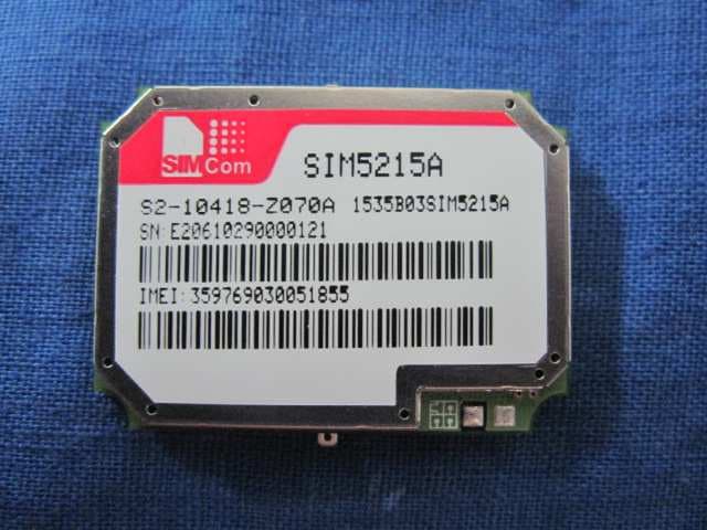
Click to zoom
Application Details
- Equipment Class
- PCB - PCS Licensed Transmitter
- Date of Grant
- Nov 04, 2010
- Application Purpose
- Original Equipment
- Date of Application
- Nov 04, 2010
- Equipment Note
- GSM/GPRS/EDGE/WCDMA module
- Frequency Range
- 1852.40000000 - 1907.60000000
- Company
- Shanghai Simcom Ltd.
- Country
- China
Documents & Files
Document Text
Text extracted from the exhibit documents filed with the FCC. Open a document above to read the original.
Users Manual
Hardware Design SIM5215A _HD_V1.02 Document Title: SIM5215A Hardware Design Version: 1.02 Date: 2010-08-26 Status: Release Document Control ID: SIM5215A _HD_V1.02 General Notes SIMCOM offers this information as a service to its customers, to support application and engineering efforts that use the products designed by SIMCOM. The information provided is based upon requirements specifically provided to SIMCOM by the customers. SIMCOM has not undertaken any independent search for additional relevant information, including any information that may be in the customer’s possession. Furthermore, system validation of this product designed by SIMCOM within a larger electronic system remains the responsibility of the customer or the customer’s system integrator. All specifications supplied herein are subject to change. NOTICE: This device complies with Part 15 of the FCC Rules [and with RSS-210 of Industry Canada]. Operation is subject to the following two conditions: (1) this device may not cause harmful interference, and (2) this device must accept any interference received, including interference that may cause undesired operation. Changes or modifications made to this equipment not expressly approved by SIMCOM may void the FCC authorization to operate this equipment. This equipment has been tested and found to comply with the limits for a Class B digital device, pursuant to Part 15 of the FCC Rules. These limits are designed to provide reasonable protection against harmful interference in a residential installation. This equipment generates, uses and can radiate radio frequency energy and, if not installed and used in accordance with the instructions, may cause harmful interference to radio communications. However, there is no guarantee that interference will not occur in a particular installation. If this equipment does cause harmful interference to radio or television reception, which can be determined by turning the equipment off and on, the user is encouraged to try to correct the interference by one or more of the following measures: • Reorient or relocate the receiving antenna. • Increase the separation between the equipment and receiver. • Connect the equipment into an outlet on a circuit different from that to which the receiver is connected. • Consult the dealer or an experienced radio/TV technician for help. SIM5215A _HD_V1.02 Hardware Design SIM5215A _HD_V1.02 26.08.2010 2 This Class [B] digital apparatus complies with Canadian ICES-003. Cet appareil numérique de la classe [*] est conforme à la norme NMB-003 du Canada. Radiofrequency radiation exposure Information: This equipment complies with FCC radiation exposure limits set forth for an uncontrolled environment. This equipment should be installed and operated with minimum distance of 20 cm between the radiator and your body. This transmitter must not be co-located or operating in conjunction with any other antenna or transmitter. Copyright This document contains proprietary technical information which is the property of SIMCOM Limited., copying of this document and giving it to others and the using or communication of the contents thereof, are forbidden without express authority. Offenders are liable to the payment of damages. All rights reserved in the event of grant of a patent or the registration of a utility model or design. All specification supplied herein are subject to change without notice at any time. Copyright © Shanghai SIMCOM Wireless Solutions Ltd. 2010 SIM5215A _HD_V1.02 Hardware Design SIM5215A _HD_V1.02 26.08.2010 3 Version history Data Version Description of change Author 2010-4-26 01.00 Origin 2010-07-19 01.01 Add RESET timing and module is waked up by DTR signal description, modify the description of PCM interface libing 2010-08-26 01.02 Add firmware update description libing SIM5215A _HD_V1.02 Hardware Design SIM5215A _HD_V1.02 26.08.2010 4 Contents Version history..............................................................................................................3 1 Introduction...............................................................................................................6 1.1 Related documents ..............................................................................................................6 1.2 Terms and abbreviations......................................................................................................7 2 Product concept.......................................................................................................10 3 Application interface...............................................................................................13 3.1 SIM5215A pin description ................................................................................................14 3.2 Operating modes ...............................................................................................................17 3.3 Power supply.....................................................................................................................18 3.3.1 Power supply pins on the board-to-board connector ....................................................................... 19 3.3.2 Minimizing power losses ................................................................................................................ 20 3.3.3 Monitoring power supply ................................................................................................................ 20 3.4 Power up and power down scenarios ................................................................................20 3.4.1 Turn on SIM5215A......................................................................................................................... 20 3.4.2 Turn off SIM5215A......................................................................................................................... 21 3.5 Power saving ..................................................................................…
Text truncated - open the document above for the full version.
Cover Letter(s)
CONFIDENTIALITY REQUEST for Certification Service in USA Federal Communication Commission Equipment Authorization Division, Application Processing Branch 7435 Oakland Mills Road Columbia, MD 21048 <2010-11-3> TO WHOM IT MAY CONCERN Pursuant to Paragraphs §0.457 and 0.459 of the Commission’s Rules (47 C.F.R.) and Section §552(b)(4) of the Freedom of Information Act, we requests confidentiality for the following products: FCC ID Model name UDV-1009092010007 SIM5215A For the product stated above, we request that the following information be held confidential: 1. Circuit diagrams, BOM, and PCBs submitted as Equipment Authorization Electronic Filing attachment: "schematics”. 2. Block diagram submitted as Equipment Authorization Electronic Filing attachment: “block diagram”. 3. Operational description submitted as Equipment Authorization Electronic Filing attachment: “operational description” 4. Parts List / Tune Up Info submitted as Equipment Authorization Electronic Filing attachment: “Parts List / Tune Up Info” The above exhibits contain our trade secrets and proprietary information that could be of benefit to our competitors. If you have any questions, please feel free to contact me at the address shown below. Sincerely, Name: Yongsheng Li Company: Shanghai Simcom Ltd. Address: Building A, SIM Technology Building No.633,Jinzhong Road,Changning Disdrict,Shanghai P.R. China 200335 Phone: 86-21-32523134 Fax: 86-21-32533020 Email: [email protected]
External Photos
Report No 109S016R-HP-US-P07V01 Page: 86 of 87 9. Attachment EUT Photograph (1) EUT Photo (2) EUT Photo
Internal Photos
Report No 109S016R-HP-US-P07V01 Page: 87 of 87 (3) EUT Photo (4) EUT Photo
RF Exposure Info
RF Exposure Evaluation Declaration Product Name : Module Model No. : SIM5215A FCC ID : UDV-1009092010007 IC : 8460A-20100909007 Applicant : Shanghai Simcom Ltd. Address : Building A, SIM Technology Building, No. 633, Jinzhong Road, Changning Disdrict, Shanghai P.R. China 200335 Date of Receipt : Sep. 14, 2010 Issued Date : Sep. 21, 2010 Report No. : 109S016R-RF-US Report Version : V2.1 The test results relate only to the samples tested. The test results shown in the test report are traceable to the national/international standard through the calibration of the equipment and evaluated measurement uncertainty herein. This report must not be used to claim product endorsement by TAF, NVLAP, NIST or any agency of the Government. The test report shall not be reproduced except in full without the written approval of QuieTek Corporation. Report No: 109S016R-RF-US Page: 2 of 7 Test Report Certification Issued Date : Sep. 21, 2010 Report No. : 109S016R-RF-US Product Name : Module Applicant : Shanghai Simcom Ltd. Address : Building A, SIM Technology Building, No. 633, Jinzhong Road, Changning Disdrict, Shanghai P.R. China 200335 Manufacturer : Shanghai Simcom Ltd. Address : Building A, SIM Technology Building, No. 633, Jinzhong Road, Changning Disdrict, Shanghai P.R. China 200335 Model No. : SIM5215A FCC ID : UDV-1009092010007 IC : 8460A-20100909007 EUT Voltage : 3.4-4.2V Trade Name : SIMCom Applicable Standard : FCC OET 65 Test Result : Complied Performed Location : Suzhou EMC Laboratory No.99 Hongye Rd., Suzhou Industrial Park Loufeng Hi-Tech Development Zone., Suzhou, China TEL: +86-512-6251-5088 / FAX: +86-512-6251-5098 FCC Registration Number: 800392 Documented By : ( Engineering ADM: Alice Ni ) Reviewed By : ( Engineering Supervisor: Marlin Chen ) Approved By : ( Engineering Manager: Dream Cao ) Report No: 109S016R-RF-US Page: 3 of 7 Laboratory Information We, QuieTek Corporation, are an independent EMC and safety consultancy that was established the whole facility in our laboratories. The test facility has been accredited/accepted(audited or listed) by the following related bodies in compliance with ISO 17025, EN 45001 and specified testing scope: The related certificate for our laboratories about the test site and management system can be downloaded from QuieTek Corporation’s Web Site : http://www.quietek.com/tw/ctg/cts/accreditations.htm The address and introduction of QuieTek Corporation’s laboratories can be founded in our Web site : http://www.quietek.com/ If you have any comments, Please don’t hesitate to contact us. Our contact information is as below: HsinChu Testing Laboratory : No.75-2, 3rd Lin, Wangye Keng, Yonghxing Tsuen, Qionglin Shiang, Hsinchu County 307, Taiwan, R.O.C. TEL:+886-3-592-8858 / FAX:+886-3-592-8859 E-Mail : [email protected] LinKou Testing Laboratory : No. 5-22, Ruei-Shu Valley, Ruei-Ping Tsuen, Lin-Kou Shiang, Taipei, Taiwan, R.O.C. TEL : 886-2-8601-3788 / FAX : 886-2-8601-3789 E-Mail : [email protected] Suzhou (China) Testing Laboratory : No. 99 Hongye Rd., Suzhou Industrial Park Loufeng Hi-Tech Development Zone., Suzhou,China. TEL : +86-512-6251-5088 / FAX : +86-512-6251-5098 E-Mail : [email protected] Taiwan R.O.C. :BSMI, NCC, TAF Germany :TUV Rheinland Norway :Nemko, DNV USA :FCC, NVLAP Japan :VCCI Report No: 109S016R-RF-US Page: 4 of 7 1. RF Exposure Evaluation 1.1. Limits According to FCC 1.1310: The criteria listed in the following table shall be used to evaluate the environment impact of human exposure to radio frequency (RF) radiation as specified in 1.1307(b) LIMITS FOR MAXIMUM PERMISSIBLE EXPOSURE (MPE) Frequency Range (MHz) Electric Field Strength (V/m) Magnetic Field Strength (A/m) Power Density (mW/cm2) Average Time (Minutes) (A) Limits for Occupational/ Control Exposures 300-1500 -- -- F/300 6 1500-100,000 -- -- 5 6 (B) Limits for General Population/ Uncontrolled Exposures 300-1500 -- -- F/1500 6 1500-100,000 -- -- 1 30 F= Frequency in MHz Friis Formula Friis transmission formula: Pd = (Pout*G)/(4*pi*r2) Where Pd = power density in mW/cm2 Pout = output power to antenna in mW G = gain of antenna in linear scale Pi = 3.1416 R = distance between observation point and center of the radiator in cm Pd id the limit of MPE, 1 mW/cm2 . If we know the maximum gain of the antenna and the total power input to the antenna, through the calculation, we will know the distance r where the MPE limit is reached. Report No: 109S016R-RF-US Page: 5 of 7 1.2. Test Procedure Software provided by client enabled the EUT to transmit and receive data at lowest, middle and highest channel individually. The temperature and related humidity: 18°Cand 78% RH. 1.3. Test Result of RF Exposure Evaluation 1.3.1. Conducted Power Analysis Table 1: Duty Cycle of TDMA Signal No. of timeslots 1 2 3 4 Duty Cycle 1 : 8 1 : 4 1 : 2.66 1 : 2 Timebased avg. power compared to slotted avg. power -9 dB -6 dB -4.25 dB -3 dB The following table shows the conducted power measured and time based average power calculated: Report No: 109S016R-RF-US Page: 6 of 7 Table 2 Frequency BandModulation Timeslots Power Measured (dBm) Time based average power (Calculated) GSM850 GMSK 1 32.55 23.55 GSM850 GMSK 2 29.24 23.24 GSM850 GMSK 3 27.35 23.10 GSM850 GMSK 4 25.84 22.84 GSM850 8PSK 1 26.61 17.61 GSM850 8PSK 2 23.43 17.43 GSM850 8PSK 3 21.58 17.33 GSM850 8PSK 4 20.38 17.38 PCS1900 GMSK 1 28.96 19.96 PCS1900 GMSK 2 25.86 19.86 PCS1900 GMSK 3 23.92 19.67 PCS1900 GMSK 4 22.84 19.84 PCS1900 8PSK 1 24.73 15.73 PCS1900 8PSK 2 21.48 15.48 PCS1900 8PSK 3 19.82 15.57 PCS1900 8PSK 4 18.35 15.35 FDD II QPSK --- 22.75 22.75 FDD V QPSK --- 23.54 23.54 Report No: 109S016R-RF-US Page: 7 of 7 1.3.2. Host Platform Analysis The MPE calculation was performed for the maximum antenna gain maybe used of stand-alone condition. According to FCC Part2.1091(c) requirement, the maximum ERP (below 1.5GHz) is 1.5W and (above 1.5GHz) is 3W. Conjunction with FCC Part22H&24E requirements, the following table shows the maximum antenna g…
Text truncated - open the document above for the full version.
Test Report
FCC Part22H&24E Test Report Industry Canada RSS-132/RSS-133 Product Name : Module Model No. : SIM5215A FCC ID : UDV-1009092010007 IC : 8460A-20100909007 Applicant : Shanghai Simcom Ltd. Address : Building A, SIM Technology Building, No. 633, Jinzhong Road, Changning Disdrict, Shanghai P.R. China 200335 Date of Receipt : Sep. 14, 2010 Test Date : Sep. 14, 2010 ~ Sep. 20, 2010 Issued Date : Sep. 21, 2010 Report No. : 109S016R-HP-US-P07V01 Report Version : V 2.0 The test results relate only to the samples tested. The test results shown in the test report are traceable to the national/international standard through the calibration of the equipment and evaluated measurement uncertainty herein. This report must not be used to claim product endorsement by TAF, NVLAP, NIST or any agency of the Government. The test report shall not be reproduced except in full without the written approval of QuieTek Corporation. Report No: 109S016R-HP-US-P07V01 Page: 2 of 87 Test Report Certification Issued Date : Sep. 21, 2010 Report No. : 109S016R-HP-US-P07V01 Product Name : Module Applicant : Shanghai Simcom Ltd. Address : Building A, SIM Technology Building, No. 633, Jinzhong Road, Changning Disdrict, Shanghai P.R. China 200335 Manufacturer : Shanghai Simcom Ltd. Address : Building A, SIM Technology Building, No. 633, Jinzhong Road, Changning Disdrict, Shanghai P.R. China 200335 Model No. : SIM5215A FCC ID : UDV-1009092010007 IC : 8460A-20100909007 EUT Voltage : 3.4-4.2V Trade Name : SIMCom Applicable Standard : FCC CFR Title 47 Part 2,TIA/EIA 603-C, RSS-GEN Issue 2 FCC Part22 Subpart H, FCC Part24 Subpart E Industry Canada RSS-132, Issue 2 Industry Canada RSS-133, Issue 5 Test Result : Complied Performed Location : SuZhou EMC laboratory No.99 Hongye Rd., Suzhou Industrial Park Loufeng Hi-Tech Development Zone., SuZhou, China TEL: +86-512-6251-5088 / FAX: +86-512-6251-5098 FCC Registration Number: 800392, IC Lab Code: 4075B Documented By : ( Engineering ADM: Alice Ni ) Reviewed By : ( Engineering Supervisor: Marlin Chen ) Approved By : ( Engineering Manager: Dream Cao ) Report No: 109S016R-HP-US-P07V01 Page: 3 of 87 Laboratory Information We, QuieTek Corporation, are an independent EMC and safety consultancy that was established the whole facility in our laboratories. The test facility has been accredited/accepted(audited or listed) by the following related bodies in compliance with ISO 17025, EN 45001 and specified testing scope: The related certificate for our laboratories about the test site and management system can be downloaded from QuieTek Corporation’s Web Site : http://www.quietek.com/tw/ctg/cts/accreditations.htm The address and introduction of QuieTek Corporation’s laboratories can be founded in our Web site : http://www.quietek.com/ If you have any comments, Please don’t hesitate to contact us. Our contact information is as below: HsinChu Testing Laboratory : No.75-2, 3rd Lin, Wangye Keng, Yonghxing Tsuen, Qionglin Shiang, Hsinchu County 307, Taiwan, R.O.C. TEL:+886-3-592-8858 / FAX:+886-3-592-8859 E-Mail : [email protected] LinKou Testing Laboratory : No. 5-22, Ruei-Shu Valley, Ruei-Ping Tsuen, Lin-Kou Shiang, Taipei, Taiwan, R.O.C. TEL : 886-2-8601-3788 / FAX : 886-2-8601-3789 E-Mail : [email protected] Suzhou (China) Testing Laboratory : No. 99 Hongye Rd., Suzhou Industrial Park Loufeng Hi-Tech Development Zone., Suzhou,China. TEL : +86-512-6251-5088 / FAX : +86-512-6251-5098 E-Mail : [email protected] Taiwan R.O.C. : BSMI, NCC, TAF Germany : TUV Rheinland Norway : Nemko, DNV USA : FCC, NVLAP Japan : VCCI Report No: 109S016R-HP-US-P07V01 Page: 4 of 87 TABLE OF CONTENTS Description Page 1. General Information ...................................................................................................... 6 1.1. EUT Description ........................................................................................................ 6 1.2. Mode of Operation .................................................................................................... 7 1.3. Tested System Details .............................................................................................. 8 1.4. Configuration of Tested System ................................................................................ 9 1.5. EUT Exercise Software ........................................................................................... 10 2. Technical Test ............................................................................................................. 11 2.1. Summary of Test Result .......................................................................................... 11 2.2. Test Environment .................................................................................................... 12 3. Peak Output Power..................................................................................................... 13 3.1. Test Equipment .......................................................................................................13 3.2. Test Setup ............................................................................................................... 14 3.3. Limit ........................................................................................................................ 14 3.4. Test Procedure ........................................................................................................ 15 3.5. Uncertainty .............................................................................................................. 16 3.6. Test Result.............................................................................................................. 17 3.7. Test Photograph ......................................................................................................22 4. Occupied Bandwidth................................................................................................... 24 4.1. Test Equipment ..............................................…
Text truncated - open the document above for the full version.
Test Setup Photos
Report No 109S016R-HP-US-P07V01 Page: 22 of 87 3.7. Test Photograph Description: ERP Test Setup Description: Substitution Antenna for ERP Test Report No 109S016R-HP-US-P07V01 Page: 23 of 87 Description: EIRP Test Setup Description: Substitution Antenna for EIRP Test Report No 109S016R-HP-US-P07V01 Page: 56 of 87 6.7. Test Photograph Description: Radiated Spurious Emission Test Setup for Below 1 GHz Description: Substitution Antenna Test Setup for Below 1 GHz Report No 109S016R-HP-US-P07V01 Page: 57 of 87 Description: Radiated Spurious Emission Test Setup for Above 1 GHz Description: Substitution Antenna Test Setup for Above 1 GHz
Contact Information
Applicant
yongsheng Li(Deputy General Manager)
Test Firm
DEKRA Testing and Certification (Suzhou) Co., Ltd.Jerry Pan
Technical Specifications
| # | Rule Parts | Frequency Range | Power Output | Emission | Tolerance |
|---|---|---|---|---|---|
| 6 | 24E | 1.85 GHz - 1.91 GHz | 189.00 mW | 4M20F9W | 65 Hz |
Other Applications from Shanghai Simcom Ltd.
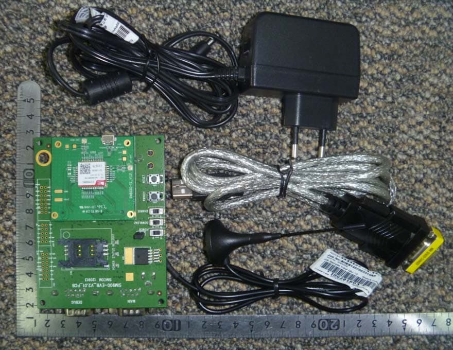
UDV-SIM800C
Mar 19, 2015GSM/GPRS Module
Equipment Class
PCB - PCS Licensed Transmitter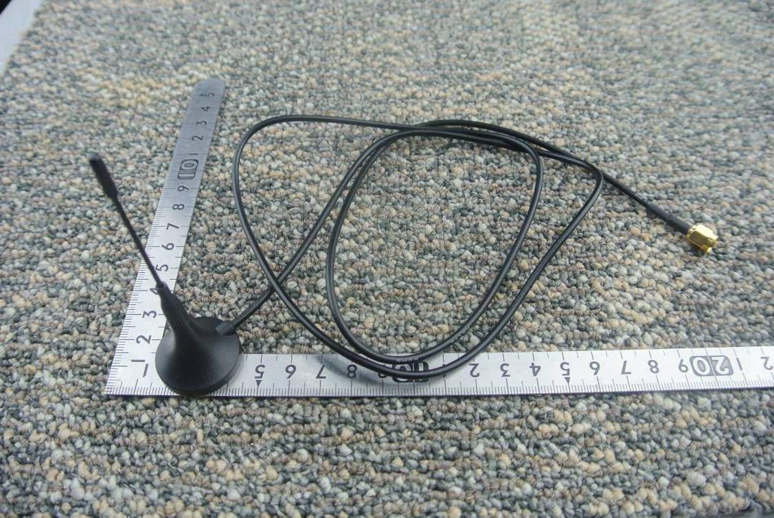
UDV-1403022014009
Sep 29, 2014WCDMA/HSDPA Module
Equipment Class
PCB - PCS Licensed Transmitter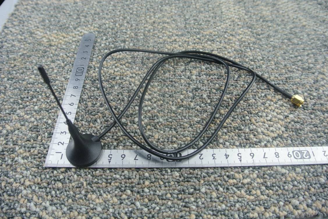
UDV-1403022014008
Sep 29, 2014WCDMA/HSDPA Module
Equipment Class
PCB - PCS Licensed Transmitter
UDV-SIM5360A
Aug 07, 2014GSM/WCDMA Module
Equipment Class
PCB - PCS Licensed Transmitter
UDV-201314
Jan 22, 2014GSM/GPRS(850/900/1800/1900MHz)+BT Wireless Data Module
Equipment Class
DSS - Part 15 Spread Spectrum Transmitter