UTLF614TWO-WAY RADIO
Unier Technology Co., Ltd.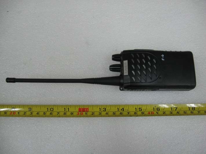
Click to zoom
Application Details
- Equipment Class
- TNF - Licensed Non-Broadcast Transmitter Held to Face
- Date of Grant
- Mar 02, 2008
- Application Purpose
- Original Equipment
- Date of Application
- Mar 02, 2008
- Equipment Note
- TWO-WAY RADIO
- Frequency Range
- 406.12500000 - 469.97500000
- Company
- Unier Technology Co., Ltd.
- Country
- China
Documents & Files
Document Text
Text extracted from the exhibit documents filed with the FCC. Open a document above to read the original.
Users Manual
, USER S MANUAL THE USER’S MANUAL User Safety, Training, and General Information READ THIS IMPORTANT INFORMATION ON SAFE AND EFFICIENT OPERATION BEFORE USING YOUR UNIER PORTABLE TWO-WAY RADIO. Compliance with RF Energy Exposure Standards The two-way radio is designed and tested to comply with a number of national and international standards and guidelines (listed below) regarding human exposure to radio frequency electromagnetic energy. This radio complies with the IEEE (FCC) and ICNIRP exposure limits for occupational/controlled RF exposure environment at duty cycles of up to 50% talk-50% listen and should be used for occupational use only. In terms of measuring RF energy for compliance with the FCC exposure guidelines, your radio radiates measurable RF energy only while it is transmitting (during talking), not when it is receiving (listening) or in standby mode. Note: The approved batteries supplied with this radio are rated for a 5-5-90 duty cycle (5% talk-5% listen-90% standby), even though this radio complies with the FCC occupational RF exposure limits at duty cycles of up to 50% talk. Complies with the following of RF energy exposure standards and guidelines: United States Federal Communications Commission, Code of Federal Regulations; 47CFR part 2 sub-part J American National Standards Institute (ANSI)/Institute of Electrical and Electronic Engineers (IEEE) C95. 1-1992 Institute of Electrical and Electronic Engineers (IEEE) C95. 1-1999 Edition International Commission on Non-Ionizing Radiation Protection (ICNIRP) 1998 Operational Instructions To ensure optimal performance and compliance with the occupational/controlled environment RF energy exposure limits in the above standards and guidelines, users should transmit no more than 50% of the time and always adhere to the following procedures: Hand-held radio operation Hold the radio in a vertical position with the microphone 5 cm away from the lips and let the antenna farther away from your head. Notices to the User •Government law prohibits the operation of unlicensed radio transmitters within the territories under government control. •Illegal operation is punishable by fine or imprisonment or both. •Refer service to qualified technicians only. WARNING: It is important that the operator is aware of and understand hazards common to the operation of any transceiver. Explosive environment(such as gases, dust, fumes, etc). Turn off your transceiver while talking on fuel, or while parked in gasoline service stations. If you require this machine to be developed or some changed, pleased connect with BFDX or your BFDX dealer. FCC Caution: This equipment has been tested and found to comply with the limits for a Class B digital device, pursuant to part 15 of the FCC Rules. These limits are designed to provide reasonable protection against harmful interference in a residential installation. This equipment generates, uses and can radiate radio frequency energy and, if not installed and used in accordance with the instructions, may cause harmful interference to radio communications. However, there is no guarantee that interference will not occur in a particular installation. If this equipment does cause harmful interference to radio or television reception, which can be determined by turning the equipment off and on, the user is encouraged to try to correct the interference by one or more of the following measures: _ Reorient or relocate the receiving antenna. _ Increase the separation between the equipment and receiver. _ Connect the equipment into an outlet on a circuit different from that to which the receiver is connected. _ Consult the dealer or an experienced radio/TV technician for help. FCC Requirements Your radio must be properly licensed Federal Communications Commission prior to use. Your Wireless dealer can assist you in meeting these requirements. Your dealer will program each radio with your authorized frequencies, signaling codes, etc., and will be there to meet your communications needs as your system expands. Precautions ٛ Only qualified technicians are allowed to maintain this product. ٛ Do not use the radio or charge a battery in explosive areas such as coal gas, dust, steam, etc. ٛ Switch OFF the radio while refueling or parking at gas station. ٛ Do not modify or adjust this radio without permission. ٛ Do not expose the radio to direct sunlight over a long time, nor place it close to heating source. ٛ Do not place the radio in excessively dusty, humid areas, nor on unstable surfaces. Safety: It is important that the operator is aware of and understands hazards common to the operation of any radio. CE Caution: Hereby, UNIER TECHNOLOGY CO., LTD. declares that this Tow-way radio is in compliance with the essential requirements and other relevant provisions of Directive 1999/5/EC and the COUNCIL RECOMMENDATION of 12 July 1999 on the limitation of exposure by the general public to electromagnetic fields (0 Hz to 300 GHz) (1999/519/EC). A copy of the DoC may be obtained through the following address. 5F, Huahan Innovation Park, Building D, Keyuan Roa, Shenzhen, China 1 1 1 1 1 1 1 1 Accessories List Accessories Adaptor Battery pack User's Manual Guarantee certification Charger Radio mainframe Antenna Quantity Before using the two-way radio, please read below safety instructions carefully. *When speaking into the microphone, please keep your mouth 2.5cm to 5cm away from microphone. *Use of accessories not originally provided or authorized by UNIER may result in risk of being exposed in the excessive electromagnetism environment without enough protection. *Please using antenna provided or authorized by UNIER. If a damaged antenna comes into contact with your skin, a minor burn can result. Please turn off your radio when you are instructed to do so. *Make sure the radio always keeping more than 15 cm away from heart pacemaker. Please do not use radio when driving. Do not store the radio in the upper of safety airbag or any place whe…
Text truncated - open the document above for the full version.
Block Diagram
1 2 3 4 5 6 78 ABCD 8 7 6 5 4 3 2 1 D CBA BLOCKDIAGRAM D400 D401 X400 7.3728MHz Q400DTC 114EE Q401 DTC 114EE R LED G LED SW SW SB TX/BUSY LAMP S402 S403 PTT MONI SCLSDA EEPROM IC401 AT24C08 5M 5M CHANNEL SW Q901 2SK 1824 CLOCK SHIFT PLL DATA EPDT CK PLL IC IC1 MBL15E03 UL 2nd LOCAL ANT 400-470MHz ENC 0 123 5C 3C6 3C6 12.8MHz X1 TCXO TOVCCN VR1 LOOP FILTER AMP Q2 2SC5108 DEV DEV D5 MA360 F. CONT F. CONT D1,D2,D3,D4 D901,D902,D903,D904 MA2S376 MA2S376 TX VCO RX VCO Q4 Q3 2SC4228 2SK508 Q6 2SC5108 BUFF AMP T/R SW Q5.Q72SJ243UMC4 RX Q8.D6 2SC4617 MA2S111 RIPPLE FILTER 5C AMPQ100 2SC4619 LO. SW 5C D100 D200 HSC277 5C 5T AMP AMP Q101 Q102 2SC4619 2SK3077 5T 5T DRIVE AMP FINAL AMP Q105 Q107 2SK3475 2SK3476 ANT SW LPF D101 HVU131 ANT SW D102D103 HSC277 DET B APC Q110 DTC 114TE 5T 5T THERMAL PROTECTION SW Q108 DTC 114EE APC SW IC100 NJM2904 5T Q109 DTA SW Q106 2SK1824 144EE BPF TUNE L208. L211D908,D909 5R 5R AMP Q203 3SK318 3SK318 BPF L203. L204. L209 D905.D906.D907 TUNE Q202 1st MIXER XF1,XF2 MCF 38.85MHz IF AMP Q201 2SC4226 5R 450KHz CF200 CF L212 DET COIL IF IC IC200 TA31136FN 5R BUSY TCXO12.8MHz 5R 38.4MHz X3 2nd LOCAL AMP Q1 2SC4649 CHARGE Q200 DTA 114EE 5RC 5R 5C 5T SW Q408DTA 123JE 5TC SAVE SW Q405UPA672T 5M Q404Q406 Q407 FP210 UMG3N 5T. 5C. REG. B REF 3C6 Q9 FS8853 5MC SWQ402DTA 114YE SB 5V REG. IC404 XC6201 T502PR UL TI TIBIBUSY BATT APC/TUNE WNRCTO SAVE 5MC5TCWNTCGLEDVCCNSHIFT 5RC AFCO MUTE EP DT CK RLEDBEEPRX TXD RXD READ/WRITE TI TIBI NJM2902V AFCO WNRC 5MS 5R VOLUME VR501VR500 SP MUTE B SW BATT POWER SW REVERSR SB B MIC D500 1SS372 LIMITER AMP 5MC WNTC Q500 2SK1824 5MC Q504 DTA 143ZE WIDE/NARROW SW IC500 NJM 2100V HPF 2SC4919 AGC/MUTE MUTE Q503 D501 SW DAN222 DET RX MIC500 5T LPF Q502 2SC4617 2SC4617 Q501 5T LPF DEV DQT BALANCE TO DEV PROTECTION D502 1SR154 SW Q304 DTC 144EE Q306 SW Q305 2SA1362 DTC 144EE MUTE SW Q9 2SK1588 AUDIO AMP IC302 KIA6278F MUTE SW Q302 2SK1824 BASE BAND SECTION IC301 LPF LPF LPF HPFHPF NJM2904V IC300 FLAT AMP 5MS 5R LIMITER DA221 WIDE/NARROW SW Q303 DTA 144EE IC101ST72321 S413 ALARM
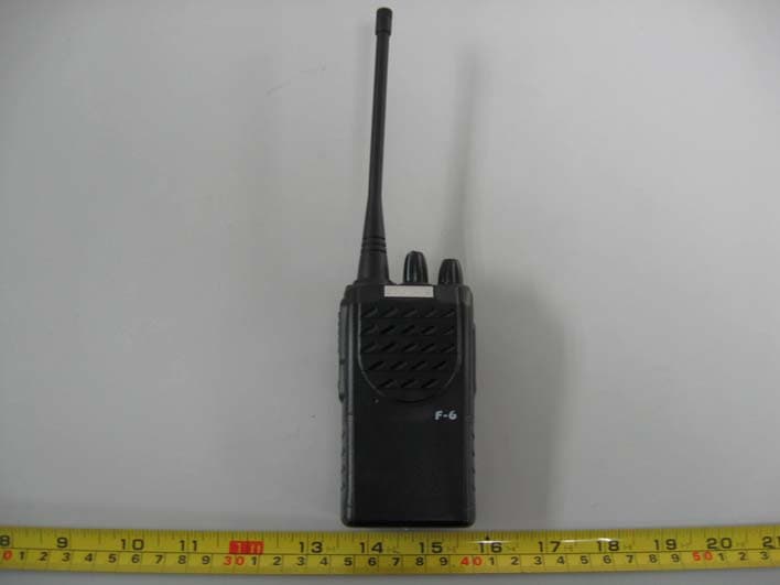
External Photos
UNIER TECHNOLOGY CO., LTD. MODEL: F6 REPORT NO.: STR08028010I FCC PART 90 EXHIBIT 2 - EUT EXTERNAL PHOTOGRAPHS EUT View 1 EUT View 2 UNIER TECHNOLOGY CO., LTD. MODEL: F6 REPORT NO.: STR08028010I FCC PART 90 EUT View 3
ID Label/Location Info
UNIER TECHNOLOGY CO., LTD. MODEL: F6 REPORT NO.: STR08028010I FCC PART 90 EXHIBIT 1- PRODUCT LABELING Proposed FCC ID Label Format Specifications: Labels are printed in indelible ink on permanent adhesive silk-screened onto the EUT or shall be affixed at a conspicuous location on the EUT. Proposed Label Location on EUT FCC ID Label Location
ID Label/Location Info
UNIER TECHNOLOGY CO., LTD. MODEL: F6 REPORT NO.: STR08028010I FCC PART 90 EXHIBIT 1- PRODUCT LABELING Proposed FCC ID Label Format Specifications: Labels are printed in indelible ink on permanent adhesive silk-screened onto the EUT or shall be affixed at a conspicuous location on the EUT. Proposed Label Location on EUT FCC ID Label Location
Internal Photos
UNIER TECHNOLOGY CO., LTD. MODEL: F6 REPORT NO.: STR08028010I FCC PART 90 EXHIBIT 3 - EUT INTERNAL PHOTOGRAPHS EUT Housing and Board View 1 EUT Housing and Board View 2 UNIER TECHNOLOGY CO., LTD. MODEL: F6 REPORT NO.: STR08028010I FCC PART 90 Solder Board-Component View 3 Solder Board-Component View 4
Operational Description
- 3 - LPF.HPF CIRCUIT DESCRIPTION 1. Frequency configuration The receiver utilizes double conversion. The first IF is 38.85MHz and the second IF is 450kHz.The first local oscillator signal is supplie d from the PLL circuit. The PLL circuit in the transmitter generates the n ecessary frequencies. Fig. 1 shows the frequencies. ANT ANT SW RF AMP MCF IF SYSTEM AF AMP SP 38.85MHz 38.4MHz X3 multiply TCXO 12.8MHz PA AMP RX TX AMP TX PLL VCO MIC AMP MIC Fig. 1 Frequency configuration 2. Receiver The receiver is double conversion superheterodyne, designe d to operate in the frequency range of 400 to 470MHz (F6U) The frequency configuration is shown in Fig.1. ①. Front-end RF amplifier An incoming signal from the antenna is applied to an RF amplifier (Q203) after passing through a transmit/receive switch circuit (D102 an D103 are off) and a 3-pole LC filter. After the signal is amplified (Q203),the signal is filtered by a band pass filter (a 3-pole LC filter) to eliminate unwanted signals before it is passed to the first mixer. The voltage of these diode are controlled by to track the MPU ANT BPF RF AMP BPF MIXER MCF IF AMP CF200 AF PA AMP D102.D103 ANT SW L208-L211 Q203 L214.L203.L204 Q202 XF201 Q201 IF.MIX.DET AF AMP IC302 SP IC200 IC300 TUNE IC403 MPU 1st Local Osc (PLL) TCXO X3 multiply Q1 WIDE/NARROW SW Q303 Fig.2 Receiver n configuration - 4 - ② . First Mixer The signal from the RF amplifier is heterodyned with the first local oscillator signal from the PLL frequency synthesizer circuit at the first mixer (Q202) to create a 38.85MHz first then fed through two monolithic crystal filters (MCFs:XF 1 and XF2) to further remove spurious signals. ③ . IF amplifier The first IF signal is amplified by Q 201,and then enters IC200 (FM processing IC).The signal is heterodyned again 450kHz second IF signal. The second IF signal is then fed through a 450kHz ceramic filter (CF200) to further elim inate unwanted signals before it is amplified and FM detected in IC200. ④ . AF amplifier The recovered AF signal obtained from IC200 is amplified by IC300 (1/4) ,Filtered by the IC300 low-pass filter (2/4) and IC300 high-pass filter (3/4) and (4/4),and de-emphasized by R303 and C306.The AF si gnal is then passed through a Wide/Narrow switch (Q303). The processed AF signal passes through an AF volume control and is amplified to a sufficient level to drive a loud speaker by an AF power amplifier (IC302). ⑤ . Squelch Part of the AF signal from the IC enters the FM IC again, and the nose co mponent is amplified and rectified by a filter and an amplifier to produ ce a DC voltage corresponding to the noise level. The DC signal from the FM IC goes to the analog port of the microprocessor (IC101).IC101 determines whether to output sounds from the speaker by checking whether the input voltage is higher or lower than the preset value. To output sounds from the speaker,IC101 sends a high signal to the MUTE and AFCO lines and turns IC302 on through Q403,Q304,Q10 and Q9.(See Fig.3) FM IF IC IC200 IF AMP DET IC300 AF AMP LPF HPF Q403 SW IC302 AF PA AMP Q9 SP SW DET HPF AMP Q304.305.10 SW IC301 LPF QT/DQT IC101 MPU Q303 W/N SW Fig.3 AF Amplifier and squelch - 5 - ⑥ . Receive signaling CTCSS/CDCSS 300Hz and higher audio frequencies of the output signal from IF IC are cut by a low-pass filter (IC300).The resulting signal enters the microprocessor (IC101). IC101 determines whether the CTCSS or CDCSS matches the preset value, and controls the MUTE and AFPAC and the speaker out sounds according to the squelch results. 3. PLL Frequency synthesizer The PLL circuit generates the first local oscillator si gnal for reception and the RF signal for transmission. ① . PLL The frequency step of the PLL circuit is 5 of 6.25kHz. A 12.8MHz reference oscillator signa l is divided at IC1 by a fixed counter to produce the 5 or 6.25kHz reference frequency. The voltage controlled oscillator (VCO) output signal is buffer amplified by Q6.thendivided in IC1 by a dual-module programmable counter. The divided signal in the phase comparator in IC1. The output signal from the phase comparator is filtered through a low-pass filter and passed to the VC O to control the oscillator frequency. (See Fig.4) ② . VCO The operating frequency is generated by Q4 in transmit mode and Q3 in receive mode. The oscillator frequency is controlled by applying the VCO control voltage, obtained from the phase comparator, to the varactor diodes (D1,D2 and D3,D4 in tran smit mode and D901,D902 an d D903,D904 in receive mode ). The T/R pin is set high in receive mode caus ing Q5 and Q7 to turn Q4 off, and turn Q3 on. The T/R pin is set low in transmit mode. The outputs from Q3 and Q4 are amplified by Q6 and sent to the buffer amplifiers. PLL DATA 12.8MHz REF OSC PLL IC IC1 1/N 1/M 5KHz/6.25KHz PHASE COMPARATOR 5KHz/6.25KHz CHARGE PUMP LPF D1.2 .3.4 D90 1.90 2.90 3.90 4 Q4 TX VCO Q3 RX VCO Q6 BUFF AMP Q5.7 T/R SW Q2 RF AM Fig.4 PLL circuit ③. UNLOCK DETECTOR If a pulse signal appears at the LD pin of IC1, an unlock condition occurs, and the DC voltage obtained from D7,R6, and C914 causes the voltage applied to the UL pin of the microprocessor to go low. When the microprocessor detects this condition, The transmitter is disabled, ignoring the push-to-talk switch input signal. (See Fig.5) - 6- SW IC101 MUTE QT/DQT TO 5C IC1 R6 IC403 D7 LD UL PLL IC C91 4 MPU Fig.5 Unlock detector circuit 4. Transmitter ① . Transmit audio The modulation signal from the microphone is amp lified by IC500(1/2),passes through a preemphasis circuit, and amplified by the other IC500(1/2) to pe rform IDC operation. The signal then passes through a low-pass filter (splatter filter) (Q501 and Q502) a nd cuts 3kHz and higher frequencies. The resulting signal goes to the VCO through the VCO modulation te rminal for direct FM modulation.(See Fig.6) ② . CTCSS/CDCSS encoder A necessary signal for CTCSS/CDCSS encoding is generated by IC101 and FM-modulated to the PLL reference signal. Since the reference OSC does not…
Text truncated - open the document above for the full version.
Parts List/Tune Up Info
Profile Code Version Ref NO. Material Code Material NameSpecificationDesignator F6(BOM) 44 10003335 0402 Resistor 33KRC0402JR-0733K6 piece R336 R514 R515 R519 R520 R707 45 10004735 0402 Resistor 47KRC0402JR-0747K19 piece R16 R22 R107 R118 R126 R141 R307 R320 R326 R330 R338 R414 R415 R421 R423 R507 R508 R612 R506 46 10005635 0402 Resistor 56KRC0402JR-0756K 1piece R335 47 10006835 0402 Resistor 68KRC0402JR-0768K1 piece R524 48 10008235 0402 Resistor 82KRC0402JR-0782K2 piece R420 R502 49 10001045 0402 Resistor 100KRC0402JR-07100K 15piece R8 R18 R21 R34 R146 R207 R313 R323 R325 R408 R533 RB03 RB08 RB12 RB17 50 10001245 0402 Resistor 120KRC0402JR-07120K5 piece R30 R306 R509 RB04 R208 51 10001545 0402 Resistor 150KRC0402JR-07150K13 piece R4 R6 R12 R14 R133 R134 R135 R136 R137 R138 R312 R914 RB11 52 10001845 0402 Resistor 180KRC0402JR-07180K5 piece R145 R202 R318 R505 RB16 53 10002245 0402 Resistor 220KRC0402JR-07220K4 pieceR411 R528 R709 R125 54 10002745 0402 Resistor 270KRC0402JR-07270K 2pieceR316 R915 55 10003345 0402 Resistor 330K RC0402JR-07330K 1 pieceR912 56 10003945 0402 Resistor 390K RC0402JR-07390K 1 pieceR701 57 10004745 0402 Resistor 470KRC0402JR-07470K3 pieceR309 R619 R206 58 10006845 0402 Resistor 680KRC0402JR-07680K1 piece R504 59 10001055 0402 Resistor 1MRC0402JR-071M 7piece R142 R304 R858 RB01 RB02 RB09 RB10 60 10001855 0402 Resistor 1.8MRC0402JR-071M8 2pieceR512 R517 61 10010R05 0603 Resistor 0ΩRC0603JR-070R3 pieceR327 L250 R120 62 10011005 0603 Resistor 10ΩRC0603JR-0710R2 pieceR115 R417 63 10014705 0603 Resistor 47ΩRC0603JR-0747R2 pieceR121 R128 64 10011815 0603 Resistor 180ΩRC0603JR-07180R1 pieceR403 65 10012215 0603 Resistor 220ΩRC0603JR-07220R1 pieceR402 66 10012715 0603 Resistor 270ΩRC0603JR-07270R2 pieceR139 R154 67 10018225 0603 Resistor 8.2kΩRC0603JR-078K2 2piece R410 R426 68 10020R05 0805 Resistor 0ΩRC0805JR-070R2 pieceR123 R127 69 1003R395 1206 Resistor 0.39ΩRC1206JR-07R393 pieceR130 R131 R132 70 10204730 Adjustable resistor POZ2AN-1-473N-T001 piece VR501 71 10206830 Adjustable resistor POZ2AN-1-683N-T001 piece VR1 72 10202240 Adjustable resistor POZ2AN-1-224N-T001 piece VR500 73 10403029 Temperator resistor 0603 3KΩ±3%32002 piece TH500 TH501 74 10425139 Temperator resistor 0603 51KΩ±3%39501 piece TH102 75 10611024 Chip R 1kΩ×4 RCA03-4D102JTP1 pieceRC1 76 piece 77 Capatiancepiece 78 11000R518 0402 Capatiance 0.5PC1005C0G1H0R5C3 pieceC47 C49 C45 79 11001R018 0402 Capatiance 1PC1005C0G1H010C 2pieceC215 C37 80 11001R518 0402 Capatiance 1.5PC1005C0G1H1R5C 2piece CB03 CB04 81 11003R018 0402 Capatiance 3PC1005C0G1H030C 4pieceC41 C54 C29 CB01 82 11004R018 0402 Capatiance 4PC1005C0G1H040C 4pieceC612 CB17 CB18 C38 83 11005R018 0402 Capatiance 5PC1005C0G1H050C 6piece C39 C42 C44 C46 CB32 CB31 84 11006R018 0402 Capatiance 6PC1005C0G1H060C 1piece CB16 85 11007R018 0402 Capatiance 7PC1005C0G1H070C 2piece C108 CB28 86 11008R018 0402 Capatiance 8PC1005C0G1H080C 1piece CB19 87 110010018 0402 Capatiance 10PC1005C0G1H100C7 piece C105 C202 C516 C907 C908 C909 C40 AmountUnits Profile Code Version Ref NO. Material Code Material NameSpecificationDesignator F6(BOM) 88 110011018 0402 Capatiance 11PC1005C0G1H110C1 pieceCB29 89 110013018 0402 Capatiance 13PC1005C0G1H130C2 pieceCB02 CB07 90 110018058 0402 Capatiance 18PC1005C0G1H180J 2pieceCB20 CB21 91 110022058 0402 Capatiance 22PC1005C0G1H220J 3pieceC100 R227 C851 92 110027058 0402 Capatiance 27PC1005C0G1H270J 5piece C118 C917 C926 C36 C935 93 110033058 0402 Capatiance 33PC1005C0G1H330J 2pieceC53 C212 94 110047058 0402 Capatiance 47PC1005C0G1H470J2 piece C929 C34 95 110056058 0402 Capatiance 56PC1005C0G1H560J2 piece C338 C35 96 110068058 0402 Capatiance 68PC1005C0G1H680J 2piece C932 C934 97 110010158 0402 Capatiance 100PC1005C0G1H101J7 piece C30 C310 C134 C208 C910 C911 C912 98 110012158 0402 Capatiance 120PC1005C0G1H121J 1pieceC933 99 110022168 0402 Capatiance 220PC1005X7R1H221K5 piece C205 C206 C334 C530 C531 100 110033168 0402 Capatiance 330PC1005X7R1H331K1 pieceC930 101 110068168 0402 Capatiance 680PC1005X7R1H681K2 piece C510 C513 102 110047168 0402 Capatiance 470pFC1005X7R1H471KT 40piece C526 C112 C25 C31 C48 C52 C55 C103 C106 C107 C110 C116 C121 C123 C132 C139 C141 C156 C203 C410 C411 C414 C416 C506 C517 C532 C920 C923 C235 CB05 CB08 CB14 CB15 CB11 CB12 CB22 CB27 CB26 C165 CB24 103 110010268 0402 Capatiance 1000pFC1005X7R1H102KT 13piece C26 C38 C43 C101 C102 C314 C407 C521 C913 C915 C916 C924 CB30 104 110033268 0402 Capatiance 3.3nFC1005X7R1H332K2 pieceC509 C512 105 110039268 0402 Capatiance 3.9nFC1005X7R1H392K1 pieceC502 106 110047268 0402 Capatiance 4.7nFC1005X7R1H472K1 piece C204 107 110056268 0402 Capatiance 5.6nFC1005X7R1H562K1 piece C308 108 110082268 040 2Capatiance 8.2nFC1005X7R1H822K1 piece C300 109 110010364 0402 Capatiance 0.01μFC1005X7R1C103KT 19piece C418 C420 C421 C422 C425 C20 C201 C210 C515 C611 C921 C931 C936 C937 C214 CB13 CB23 CB25 CB09 110 110018368 0402 Capatiance 18nFC1005X7R1H183K2 pieceC301 C508 111 110022364 0402 Capatiance 223C1005X7R1C223K1 pieceC518 112 110027364 0402 Capatiance 273C1005X7R1C273K 3pieceC500 C501 C524 113 110033364 0402 Capatiance 333C1005X7R1C333K4 piece C27 C318 C503 C607 114 110047364 0402 Capatiance 473C1005X7R1C473K8 piece C306 C319 C335 C511 C514 C606 C9 C50 115 11006838 0402 Capatiance 683C1005X5R1A683KT1 pieceC520 116 110010464 0402 Capatiance 0.1μFC1005X5R1C104K18 piece C14 C104 C113 C207 C209 C211 C213 C303 C305 C525 C703 C914 C404 C918 CB06 C853 C854 C855 117 110047483 0402 Capatiance 474C1005Y5V1A474Z2 piece C609 C610 118 110010562 0402 Capatiance 105JRM155R60G105KE19D 2pieceC28 C603 119 11011R018 0603 Capatiance 1pFC1608C0G1H010C 3pieceC149 C950 C154 120 11011R518 0603 Capatiance 1.5pFC1608C0G1H1R5C2 pieceC147 C151 121 11012R018 0603 Capatiance 2pFC1608C0G1H020C 4pieceC144 C952 C955 TC2 122 11013R018 0603 Capatiance 3pFC1608C0G1H030C1 pieceC153 123 11015R018 0603 Capatiance 5pFC1608C0G1H050C3 piece C142 C953 C150 AmountUnits Profile Code Version Ref NO. Material Code Material Nam…
Text truncated - open the document above for the full version.
Parts List/Tune Up Info
TURN UP INFORMATION INTRUMENT: Standard Signal Generator(SSG) 1set Digital Voltmeter 1set Power Meter 1set Frequency counter 1set Distortion meter 1set Spectrum analyzer 1set Oscilloscope 1set Audio Generator (AG) 1set AF Volt Meter 1set Tracking Generator 1set 8Ω Dummy Load 1set Regulated power supply 1set Ammeter 1set Deviation Meter 1set Adjustment: Some items can be adjusted in conventional mode and the others in manual mode Turn the power on to enter conventional mode. Common Section Measurement Adjustment Item Condition Test Instrument TerminalPartMethod Specification/Remarks 1.Setting 1) BATT Terminal Voltage : 7.2V 2) SSG standard Modulation [WIDE]MOD:1kHz,DEV:3kHz [NARROW]MOD:1kHz,DEV:1.5kH z 1)CH : HI TC2 3.6 V ±0.1V 2.VCO Lock voltage RX 2)CH : LO CHECK ≥0.9V 3)CH : HI PTT : ON TC1 3.8 V ±0.1V 3.VCO Lock voltage TX 4)CH : LO PTT : ON Power Meter DVM ANT CV CHECK ≥0.7V Transmitter Section: Measurement Adjustment Item Condition Test Instrument Terminal Test Instrument Terminal Measurement 1. Frequency Adjustment 1)CH : HI 2)PTT : ON Frequency counter ANT VR1 469.975MHz ±50Hz 2. High Power Adjust TEST CH: LO Center HI ( 3 POINT ) BATT Voltage:7.2V PTT : ON 3.7W(Conducted) ≤1.6A 3. Low Power Adjust(N/A) BATT terminal Voltage :7.2V PTT : ON Power Meter Ammeter Max deviation adjust [ wide ] TEST CH: Center AG : 1kHz / 120mV Deviation meter filter LPF : 15kHz HPF : OFF PTT : ON 4.6kHz (According to t h lager+,-) ±50Hz Error:3.8~4.8KHz 4. [ narrow] TEST CH : Center PTT : ON Power meter Deviation meter Oscilloscop e AG AF VTVM ANT SP / MIC connecto r Programmin g software : U10 2.3kHz (According to t h lager+,-) ±50Hz DQT Balance adjust [ wide TEST CH: LO MID HI ( 3 POINT ) LPF : 3kHz HPF : OFF PTT : ON 5 . [ narrow ] TEST CH : Center PTT : ON Power mete r Deviation meter Oscilloscop e AG AF VTVM ANT Programming software : U10 Make the demodulation wave into square waves 6. QT deviation adjust [ wide ] TEST CH: LO MID HI ( 3 POINT ) LPF : 3kHz HPF : OFF PTT : ON Power meter Deviation meter Oscilloscop e AG AF VTVM ANT Programming software : U10 0.75kHz ±100Hz [ narrow ] TEST CH : Center PTT : ON 0.35kHz ±100Hz 7. DQT deviation adjust TEST CH : Center Low High ( 3 points ) LPF : 3kHz HPF : OFF PTT : ON 0.75kHz ±100Hz [ narrow ] TEST CH : Center PTT : ON 0.35kHz ±100Hz Receiver Section Measurement Adjustment Item Condition Test Instrument Termi l Part Method Specification/Remarks 1. BPF Wa v e adjust (1)Center frequency Spectrum analyzer setting Center-f : 440.125MHz Span : 50MHz RBW : 300kHz VBW : 10kHz ATT : 5dB (2)High-edge frequency Spectrum analyzer setting Center-f: 469.975 MHz (3)Low-edge frequency Spectrum analyzer setting Center-f : 406.125 MHz Spectrum analyzer ANT BPF Programming software : U10 Adjust the waveform as shown to the right ) Sensitivity [ wide ] TEST CH : LOW Center High SSG output : -119dBm (0.3μV) SSG MOD : 3.0kHz 2. [ narrow] TEST CH : Center SSG output : -117 dBm (0.4μV) SSG MOD : 1.5kHz check 12dB SINAD or more SQL1 (Threshold) writing [ wide ] TEST CH : Center LOW High SSG output : -123 dBm (0.16μV) SSG MOD : 3.0kHz 3. [narrow ] TEST CH : Center SSG OUTPUT : -122 dBm (0.18μV) SQL9 (Tight writing [ wide ] TEST CH : Center Low High SSG output : -117 dBm (0.3μV) 4. [ narrow ] TEST CH : Center SSG output : -116 dBm (0.35μV) SSG DVM Oscilloscope AF VTVM ANT write Squelch open Error: ±1.5dB 5. BATT Detection Writing BATT Terminal voltage : 5.6V DVM ANT BATT termin al Programming software : U10 writing BATT Terminal voltage : 5.6V
Schematics
1 2 3 4 5 6 7 8 9 10 11 12 13 14 15 16 17 18 19 A B CD EF G 19 18 17 16 15 14 13 12 11 10 9 8 7 6 5 4 3 2 1 G FE DC B A Title Number Revision Size D Date: 3-Mar-2008 Sheet of File: E:\unier-f5\F5U21412GPS-20071201A.DDBDrawn By: C907 10p C908 10p L4030.22u C410 470p C417 1u R411 220k R407 1k C411 470p R417 10 R402 220 R403 180 R426 8.2K R410 8.2K C406 470P C402 470P C90.033U C14 104 R12150K R113.9K C27 0.033U C23 10u 6.3v R8 100K c4280.01u C281u L17 220n(-38) C200.01u R4 150k R14150K C31 100P L9 3.3u(-86) L11 3.3u(-86) *C35 *C36 TC1 0-10P *L14 *C41 *C44 C45 10P(C) R500 4.7K R5014.7k R513 47K R518 10K R509 120K C501 0.027u C500 0.027u C30 1000p L8 100n (-77) L12 100n (-77) C3418p *C37 TC2 0-10P *L13 *C38 *C42 *C39 C408 10u 6.3v *R25 L20 3.3u (-86) C43 1000P L15 220n (-77) A0 1 A2 2 A2 3 GND 4 VCC 8 TEST 7 SCL 6 SDA 5 IC401AT24C08 R400 4.7k R40110K R4051K EEPROM C471p(B) C490.5P(B) C46 470P R26100 R34 100k C48 470p L19 R31 100 C52 470P R32 4.7K C55 470P R331K 1 1 2 2 L21 22n (-77) R30 120K C536p C543P (B) R408100k L10 R2247K C50 0.033U Q3 2SK508NV(K52) IN OUT GND IC404XC6201T502PR *L18 C100 22P R100 3.3K R101 10k R102 270 R103 3.3K R104 10 C101 470P L100 22n(-77) C103 470P C102 470P C104 0.1u C6070.033U C105 6P R1053.3K R213 0 C106470P R10747K R108 330 L101 10n(-77) C107470P R109 22 R1063.3K C1087P C109 470P 1 1 2 2 3 3 Q102 2Sk3077 R110 680 R113 330 L102 15n R1121.5K C110 470P L103 C111 6P R115 10 C114 470P R120 0 G G Q105 2sk3475 C116 1000P C113 0.1u L104 1u (-76) L105 C120 470P *L119 C11824P (G) C119 1000p R125 47K R128 47 C123 1000P R126 47K C121470P D D S S G G Q107 2sk3476 12 543 Q7UMC4 C40 0.5P(B) C950 1P (B) C130 R1230 C954 3P C955 0.5P C138100P D101HVU131TRF *C142 C145470P *C147 L1124T *L113 *L114 *C150 *C153 C149 1P(B) *C151 *C154 *C155 L118 1u (-81) L106 8T L107 C125470P C128 0.01u C1310.1u C126 1u C129 470P L109220N(-54) R139 270 R154 270 L110 4T C143 470P C1442P(B) R147 0 RF AMP RF SW RF SW T:1.08VR:1.31V TX PRE DRIVE T:4.84V Q102 TX DRIVE C157470P C156 0.1u D D S S G G Q106 2SK1824 14 85 - + + - IC100NJM2904V R136 150K R135 150k R133 150K R1320.39 R134150k R137 150K(D) R138150K(D) R14010k R1421M R145180K R141 47K R1430 R146 100K C134 100P C132 470P R1442.2k C141 470P R1310.39 R130 0.39 C139 470P RF AMP T:2.41V R:2.38V C427470P Q408 DTA123JE C421 0.01u C424 1u R312150K C305 0.1U C306 R303 0 C301 0.018u L401 C416 470P C414470P R406 2.2K R615 3.9K C300 8200P R3025.6K R301 5.6K C3131u R306 120K R329 0 R338 47K R307 47K R305 18K R3041M OSC1 1 OSC2 2 MIXO 3 VCC 4 IFI 5 DEC 6 FILO 7 FILI 8 IF 9 QUAD 10 IFO 11 RSSI 12 NDET 13 NREC 14 E 15 MIXI 16 IC200 TA31136FN R206 180K C205220PC206220P R201 3.9K R202180KR2043.3K C204 4700P C3030.1u R309 470K R308 10K C304 10u6.3V R203 3.3K C202 10P C203 470P IF SYSTEM C207 0.1u 1 5 2 3 4 CF200 LTM450FW C430 1u R20010 C200 10u 6.3v C2010.01u 1 1 2 2 L212 C208 27P R205 15K C2100.01u R207100K C2130.1u C211 0.1u C209 0.1u C212 33P R210 470 R208 680K C2141000P C223 CB301000P RB15 330R LB10680NH LB09 470NH 1 1 2 2 4 4 3 3 Q202 3SK318 RB18 3.3K CB29 11P CB24470P CB25 103 R214 10K C224470P R2092.7K CB28 7P CB27470P LB0612NH R117 12K R118 47k R121 47 C1276.8u10V RB13 330R RB14 47 C307 10u 6.3V LB05 5T CB21 18P CB16 6P CB11 470P LB02 150NH RB06 47R RB03 100K RB10 1M RB05 150 CB15470P CB10470P Q2033sk318 LB01 3T LB04 5T L2066.8NH CB2018P CB19 8P RB02 1M RB091M CB07 13P CB0213P CB013P R334 10 R332 150 C330 100P C335 0.047u C334220P C337 100u 6.3V R3312.2KC327 0.1u R330 47K R3398.2K R333 3.9K 1 1 3 3 2 2 D500 1SS372 R532820 1 1 2 2 3 3 Q503 2SC4919 C5240.027u C525104 L500 R534 1.8K R535470 R537 100 C523 2.2uf R530 100 14 85 - + + - IC500NJM2100V C522 0.1u C521 1000P R529 18K R533 100K C526470P 1 1 2 2 SPEAKER 1 1 2 2 MI C500 C527 10u 6.3V C531220P C532 470P R531 0 C529 470P C530 220P L501 C528 470P + 1 - 2 BT1BATTERY C5200.022u(J) R528 750K R542 0 R526 15K(D) R52715K(D) C518 0.022u(J) R525 1.5K R5236.8K C517 470P C516 10P R524 51K R522 1.8K R521 3.3K C5140.047u R520 33K D D S S G G Q500 2SK1824 C5123300P R519 33K R516 10K R5171.8M C5150.01u C513 680P(J) C506 470P C5110.047u R51533K C509 3300P R514 33k R511 10k R512 1.8M C510 680P(J) R5103.3k C508 0.01u C5072.2u R5085.6K R507 47K R543 0 VR501 47K C505 1u *R503 *R505 *R504 *R506 C3141000P R323100K R318180k C319 0.047u(J) C33856P R325 100K C3180.033u R32047K C308 5600P R316270K R313100K D300DA221 C311 10u 6.3v R44210 C420 0.01u C4220.01u C4180.01u C425 0.01u R41547K R41447K R421 47K R423 47K R430 2.2K R5483.3K L4020.22u(-86) R418 2.2k 1 1 2 2 S402PTT R413 1K R433 2.2K R3281K ENC0ENC1ENC2ENC3 10 10 9 9 8 8 7 7 6 6 5 5 4 4 3 3 2 2 1 1 1 10 4 5 7910 CHANNEL SWICHPOWER SWICHAUDIO VOLUME CN400 AUDIO OUTAUDIO INENC0ENC1BATTY INGNDBATTY OUTENC3ENC2 GNDAUDIO INAUDIO OUTBATTY IN BATTY OUT TP2 RB19 1K R11K R502 82K R541 4.7K C5023900P C5030.033U R342 4.7K R416 4.7K R5361K RESET SW *R127 C235470P R35 3.9k C407 1000p C438 1000p R28 C519 10u6.3V D901MA2S367 D903MA2S 367 D904MA2S367 D902MA2S367 *D5 1 1 2 2 D6 MA2S111 D D G G S S Q5 2SJ243 Q8 2SC4617(S) C C B B E E Q6 2SC5108(Y) C C B B E E Q100 2SC4619 D200 HS C277TRF D100 HSC277TRF C C B B E E Q101 2SC4619 1 1 2 2 D103HSC277TRF 2 2 3 3 1 1 Q108 DTC114EE 1 1 3 3 2 2 Q109DTA144EE Q304 DTC144EE B B E E C C Q305 2SA1362 2 2 1 1 …
Text truncated - open the document above for the full version.
Contact Information
Applicant
Victoria Wu(Manager)
Test Firm
Solid Industrial Co., Ltd.Yang Dengfang
Technical Specifications
| # | Rule Parts | Frequency Range | Power Output | Emission | Tolerance |
|---|---|---|---|---|---|
| 2 | 9 | 406.125 MHz - 469.975 MHz | 3.72 W | 16K0F3E | 5 ppm |
Other Applications from Unier Technology Co., Ltd.
UTLF6
Oct 18, 2007TWO-WAY RADIO
Equipment Class
TNF - Licensed Non-Broadcast Transmitter Held to Face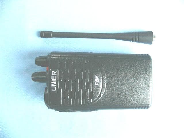
UTLF8
Feb 14, 2007TWO-WAY RADIO
Equipment Class
TNF - Licensed Non-Broadcast Transmitter Held to Face