UU3FC301DU1UHF DATA RADIO
Shenzhen Friendcom Technology Co., Ltd.
Click to zoom
Application Details
- Equipment Class
- TNB - Licensed Non-Broadcast Station Transmitter
- Date of Grant
- Jul 01, 2012
- Application Purpose
- Original Equipment
- Date of Application
- Jul 01, 2012
- Equipment Note
- UHF DATA RADIO
- Frequency Range
- 406.10000000 - 470.00000000
- Country
- China
Documents & Files
Document Text
Text extracted from the exhibit documents filed with the FCC. Open a document above to read the original.
Users Manual
FC-301/DRFLinkModule USERMANUAL SHENZHENFRIENDCOMTECHNOLOGYDEVELOPMENTCO.,LTD ADD:6/F,17Building,GuangqianIndustrialPark,LongzhuRoad,XiliTown, Nanshan,ShenzhenCity518055P.R.CHINA. TEL:+86-755-86026600+86-755-86026192FAX:+86-755-86026300 E-MAIL:[email protected] WEBSITE:www.friendcom.com -1- MANDATORYSAFETYINSTRUCTIONSTOINSTALLERSANDUSERS UseOnlymanufacturerordealersuppliedantennas. Antennaminimumsafedistance:35cm. Antennasusedforthistransmittermustnotexceedanantennagainof3dBi. TheFCC(FederalCommunicationsCommission)hasadoptedasafety standardforhumanexposuretoRFenergywhichisbelowtheOSHA (OccupationalSafetyandHealthAct)limits. Antennamounting:Theantennasuppliedbythemanufacturerorradiodealer mustnotbemountedatalocationsuchthatduringradiotransmission,any personcancomecloserthantheaboveindicatedminimumsafedistancetothe antenna(i.e.35cm). TocomplywithcurrentFCCRFExposurelimitations,theantennamustbe installedatorexceedingtheminimumsafedistanceindicatedabove,andin accordancewiththerequirementstotheantennamanufacturerorsupplier. Vehicleinstallation:Theantennacanbemountedatthecenterofavehiclemetal roofortrunklidiftheminimumsafedistanceisobserved. Antennasubstitution:Don’tsubstituteanyantennafortheonesuppliedor recommendedbythemanufacturerorradiodealer.Youmaybeexposing person(s)toexcessiveradiofrequencyradiation.Youmaycontactyourradiodealer orthemanufacturerforfurtherinstructions.Warning Maintainaseparationdistancefromtheantennatoperson(s)atleast108cm. -2- Caution: Changesormodificationsnotexpresslyapprovedbythepartyresponsiblefor compliancecouldvoidtheuser'sauthoritytooperatetheequipment. Thisdevicecomplieswithpart15oftheFCCRules.Operationissubjecttothe followingtwoconditions:(1)Thisdevicemaynotcauseharmfulinterference,and(2) thisdevicemustacceptanyinterferencereceived,includinginterferencethatmay causeundesiredoperation. Note:Thisequipmenthasbeentestedandfoundtocomplywiththelimitsfora ClassBdigitaldevice,pursuanttopart15oftheFCCRules.Theselimitsare designedtoprovidereasonableprotectionagainstharmfulinterferenceina residentialinstallation.Thisequipmentgenerates,usesandcanradiateradio frequencyenergyand,ifnotinstalledandusedinaccordancewiththeinstructions, maycauseharmfulinterferencetoradiocommunications.However,thereisno guaranteethatinterferencewillnotoccurinaparticularinstallation.Ifthis equipmentdoescauseharmfulinterferencetoradioortelevisionreception,which canbedeterminedbyturningtheequipmentoffandon,theuserisencouragedtotry tocorrecttheinterferencebyoneormoreofthefollowingmeasures: Reorientorrelocatethereceivingantenna. Increasetheseparationbetweentheequipmentandreceiver. Connecttheequipmentintoanoutletonacircuitdifferentfromthattowhichthe receiverisconnected. Consultthedealeroranexperiencedradio/TVtechnicianforhelp. -3- Note:Themanufacturerisnotresponsibleforanyradioortvinterferencecausedby unauthorizedmodificationstothisequipment.Suchmodificationscouldvoidthe user’sauthoritytooperatetheequipment. -4- TABLEOFCONTENTS TABLEOFCONTENTS..................................... . 01 .. INTRODUCTION ...........................................02 FEATURES ................................................02 SPECIFICATION ...........................................02 WIRINGDIAGRAM .........................................8 TROUBLESHOOTINGGUIDE ................................10 FACTORYDEFAULTSETTING ..............................11 INTRODUCTION -5- TheFC-301/DRFLinkModulesfromFriendcomutilizesthelatesttechnology initsdesignandmanufacturing.It’sPLL(PhaseLockLoopSynthesizer)/ microprocessorcontrolled,andoffersonetofivewattsofpowerwith16channel capability.MultiplefunctionsincludingACaudiocoupling,1200to9600baud ratesGMSKandFSKmodulationcapabilityarestandardinthisfully programmablewidebandwidthRFLinkModuleunits. FEATURES ● 16Channels ● 1-5WattProgrammableRFOutput ● 12.5kHzProgrammableChannelSpacing SPECIFICATIONS GENERAL EquipmentType.......................................DataRadio FrequencyBand...................................................UHF ChannelSpacing....................................12.5KHzprogrammable RFOutputPower.....................................1W-5WProgrammable Modulationtype......................................8K5F3E -6- IntermediateFrequency..............................45.1MHz&455KHz NumberofChannels..................................16 FrequencySource.....................................Synthesizer OperationRating.......................................Intermittent 5:5:90(TX:RX:Standby) PowerSupply..........................................12.5VDCNominalVoltage TemperatureRange Storage.............................................from–40°Cto+80°C Operating..........................................from–30°Cto+60°C CurrentConsumption Standby(Muted)................................. ≤ 40mA Transmit5WattsRFPower.....................<1.5A Transmit1WattRFPower.......................<0.8A Dimensions...................................(120mm)Lx(60mm)Wx(20mm)H Weight..................................................... ≤ 150grams TRANSMITTER SustainedTransmission.................................Nominalconditions -7- Time:51030sec Power:>95%>95%>90% FrequencyError......................................... ± 2.5ppm FrequencyDeviation: 12.5kHzChannelSpacing........................ ≤± 2.5kHz, AudioFrequencyResponse.........................Within+1/-3dBof6dBoctave @300Hzto2.55kHzfor12.5kHzC.S AdjacentChannelPower 12.5kHz.............................................<60dBc@NominalCondition <55dBc@ExtremeCondition ConductedSpuriousEmission.........................<-36dBM ModulationSensitivity..................................100mVRMS@60%peakDev. Hum&Noise: 12.5kHzChannelSpacing..........................>36dB(withPOSPH) ModulationSymmetry...................................<10%PeakDev@1kHzinput fornominaldev+20dB LoadStability..........................................Nooscat>=10:1VSWRall phaseanglesandsuitableantenna Nodestroyat>=20:1allphaseangle RECEIVER -8- Sensitivity(12dBSinad)......…
Text truncated - open the document above for the full version.
Cover Letter(s)
ShenzhenFriendcomTechnologyDevelopmentCo.,Ltd. 6/F,17Building,GuangqianIndustrialPark,LongzhuRoad,XiliTown,NanshanDistrict,ShenzhenCity,China June26,2012 FederalCommunicationsCommission Re:FCCID:UU3FC301DU1 Applicant: ShenzhenFriendcomTechnologyDevelopmentCo.,Ltd. Subject:justificationletterforexpandedfrequencyrange400–470MHz ToWhomItMayConcern: AccordingtoKDB634817... Youhaveaskedtheapplicantforjustificationtohavethe400–470MHzfreqrangeappear onhefaceoftheFCCGrantofCertificationforaPart90Certification.Thisfrequencyrange containsfrequenciesregardedasusual&customarybyUnitedStatesFederalGovernmentand itsvariousdepartments,userorganizationsandthemilitarytoappearonthefaceofthe equipmentGrantofCertification. (1)TheapplicantplanstoensurethatUSAusers,otherthanthosespecificallyidentifiedin thisletter,notoperatewithinbandswhicharenotallowedbythePart90,ascontrolledbythe users’FCCstationlicense. (2)ThisdevicewillnotbemarketedtoUSAusers,otherthanthoseidentifiedintheletter, namelytheUSGovernmentanditsvariousdepartments&military,foroperationinfrequency rangeoutofPart90. – 2 –June26,2012 Sincerely, ------------------------------- TonyCui/GeneralManager Tel:+86-755-86026800 Fax:+86-755-86026300
Cover Letter(s)
ShenzhenFriendcomTechnologyDevelopmentCo.,Ltd. 6/F,17Building,GuangqianIndustrialPark,LongzhuRoad,XiliTown,NanshanDistrict,Shenzhen City,China AGENCYAUTHORIZATIONLETTER FCCID:UU3FC301DU1Date:June20,2012 FederalCommunicationsCommission AuthorizationandEvaluationDivision 7435OaklandMillsRoad Columbia,MD21046 Towhomitmayconcern: We,theundersigned,herebyauthorizeShenzhenCTLElectromagnetic TechnologyCo.,Ltd.(MR.TracyQi)onourbehalf,toapplytotheFederal CommunicationsCommissiononourequipment.Anyandallactscarriedout byShenzhenCTLElectromagneticTechnologyCo.,Ltd.(MR.TracyQi)on ourbehalfshallhavethesameeffectasactsofourown.Thisauthorization expiresonJune19,2013. ThisistoadvisethatweareinfullcompliancewiththeAnti-DrugAbuse Act.We,ShenzhenFriendcomTechnologyDevelopmentCo.,Ltd.arenot subjecttoadenialoffederalbenefitspursuanttoSection5301ofthe Anti-DrugActof1988,21USC853a,andnopartytotheapplicationis subjecttoadenialoffederalbenefitspursuanttothatsection. Sincerely, ------------------------------- TonyCui/GeneralManager Tel:+86-755-86026800 Fax:+86-755-86026300
External Photos
6 . E x t e r n a la n dI n t e r n a lP h o t o so f t h eE U T ExternalPhotos
ID Label/Location Info
Applicant:ShenzhenFriendcomTechnologyDevelopmentCo.,Ltd. FCCID:UU3FC301DU1 ModelName:FC-301/D FCCID:UU3FC301DU1 TheFCCidentifierismarkedintheproductlabelandtheRFexposurecautionlabelisattachedontherearsideof thecabinet.Theusernoticeandwarningstatementaredescribedintheusermanual.. ProposedLabelLocationonEUT
Internal Photos
InternalPhotos
Operational Description
OPERATION OPERATION OPERATION OPERATIONDESCRIPTION DESCRIPTION DESCRIPTION DESCRIPTION The The The TheBase Base Base BaseBand Band Band Bandsignal signal signal signalcircuits circuits circuits circuits ItcontainstheCPU,powercircuit,TXsignalcircuit,RXsignal circuit. The The The TheCPU CPU CPU CPUcircuit circuit circuit circuitand and and andpower power power powercircuit circuit circuit circuit FromBlockDigramabove:TheDCpowerwasregulatedto8volt byIC500,andsuppliedtotheRFpart.IC504convert8voltto5volt andsupplytoIC510.Q500isRXpowersupplyswitch,Q502isTX powersupplyswitch.IC501supply3.6VtoPLLIC.Channelscan beselectedbytheswitch(CF3).IC510controlsdigitalfrequency synthesizebyPLLSTR,PLLDATAandPLLCCK. TheCPUSQpindetectthesignalfromPIN14ofIC2.whenthereis noreceiveingsignal,theinputlevelisabout1.2V,andPIN8of IC510outputhighlevel(5V).Whendetectinputreceivingsignal,the inputlevelisabout0V,andPIN8ofIC510outputlowlevel(5V). TX TX TX TXsignal signal signal signalcircuit circuit circuit circuit FromtheaboveBlockDiagram:IC801isaudio/DataandUART signalswitch.WhentheSWpinishigh,audio/datasignalcango throughIC801.S1isaswitchbetweenaudioanddatainput,when transmitaudio,MICINportisshorted,whentransmitdata,DATA INportisshorted.Asitwasdatasignalitwillpassthrough DATA-INportandamplifiedbyU1A,thenitwascouplingbyC431 andpasstoU1Bforamplifyagain;asitwasaudiosignalitwillpass throughMIC-INportandamplifiedbyU1B;thenitwilldivideinto twosignal,onewillcouplingbyC405R407andfedtoTCXOfor TXmodulation;theotheronewasamplifiedbyU1C,aftercoupling byC428,R404,C427;thevoicesignalisfilteredbyU1Dwhichisa lowpassfilter,theoutputofU1DisthenfedtoVCOforTX modulationaftercouplingbyC415,R403again.Q401isa Wideband/narrow-bandswitch. RX RX RX RXsignal signal signal signalcircuit circuit circuit circuit FromtheaboveBlockDiagram;TheresultingAFsignalfromIC2 entersbasebandprocessingchipU2.FirstcouplingbyC412and amplifiedbyU2A,thenitisfilteredbyU2Bwhichisalowpass filter.AfterU2B,onesignalpassthroughIC801andsendtoCOMpin 2,onesignalisamplifybyaudioamplifierIC8,andsenttothehorn directly.Q403isaaudioPAswitch. RF RF RF RFcircuit circuit circuit circuit MainincludePLLcircuit/TXcircuit/RXcircuit PLL PLL PLL PLLFrequency Frequency Frequency FrequencySynthesizer Synthesizer Synthesizer Synthesizer FromtheaboveBlockDiagram:PLLcircuitgeneratesthefirstlocal oscillatorsignalforreceptionandRFsignalfortransmission. 1. 1. 1. 1.PLL PLL PLL PLLCircuit Circuit Circuit Circuit StepfrequencyofPLLcanbe5.0KHzor6.25KHz.A13MHz referenceoscillatorsignalisdividedatIC301byacounterto generatea5.0KHzor6.25KHzreferencefrequency.Outputsignal fromVCOisbufferamplifiedbyQ301anddividedatIC301bya frequencydivider.Thedividedsignaliscomparedwith5.0KHzor 6.25KHzreferencesignalinthephasecomparatorofIC301.The outputsignalfromphasecomparatorisfilteredthroughalowpass filter(Q320/Q321/R39/C328/R318/R31/C327/R316/C326)to generatealevelD.C.,andthelevelD.C.controlsoscillator frequencybycontrollingVCO. 2. 2. 2. 2.VCO VCO VCO VCO TheoperatingfrequencyisgeneratedbyQ302intransmitmodeand byQ307inreceivemode.Operatingfrequencygenerateacontrol voltagebyphasecomparatortocontrolvaractordiodessothatthe oscillatorfrequencyisconsistentwiththeMCUpreset frequency(D301 、 D302 、 D303andD304intransmitmode,and D307 、 D308 、 D309andD310inreceivemode).T/Rpinissethigh levelinreceivemode,andlowlevelintransmitmode.Theoutput fromQ302andQ307isamplifiedbyQ304andsenttobuffer amplifier. 3. 3. 3. 3.Unlock Unlock Unlock UnlockDetector Detector Detector Detector AnunlockconditionappearsiflowlevelappearsatMUXOUTpin ofIC301.Transmissionisforbiddenifthisconditionisdetectedby CPUIC510. Receiver Receiver Receiver Receiver Thereceiverutilizesdoubleconversionsuperheterodyne (UHF)/(VHF). 1. 1. 1. 1.Front-end Front-end Front-end Front-endRF RF RF RFAmplifier Amplifier Amplifier Amplifier ThesignalfromantennaisamplifiedatLNA(Q15)afterpassing throughatransmit/receivecircuitandabandpassfilter ( D211/D212/D241/C264/C260/L25/L26 ) .Beforepassingthefirst mixer ( T3 、 T4 、 TC3 ) ,theamplifiedsignalisfilteredthroughanother bandpassfilter ( D208/D209/C240/C257/C258/L23/L24 ) toremove unwantedsignals. 2. 2. 2. 2.First First First FirstMixer Mixer Mixer Mixer ThesignalfromRFamplifierismixedwiththefirstlocalfromPLL frequencysynthesizercircuitatthefixmixer(T3 、 T4 、 TC3)tocreate a45.1MHzfirstIFsignal.ThefirstIFsignalisthenamplifiedby Q13andfedthroughacrystalfilter(XF1)tofurtherremove unwantedsignals. 3. 3. 3. 3.IF IF IF IFAmplifier Amplifier Amplifier Amplifier ThefirstIFsignalisamplifiedbyQ13beforepassingthrough crystalfilterandbyQ12aftercrystalfilterandthenentersIF processingchipIC2.ThesignalfromIC2ismixedwiththesecond oscillatorsignalagaininIC2tocreatea455KHzsecondIFsignal. ThesecondIFsignalthenpassesthrougha455KHzceramicfilter (wideband:CF2 , narrowband:CF1)toeliminateunwantedsignals beforeitisamplifiedanddetectedinIC2. 4. 4. 4. 4.Narrowband/Wideband Narrowband/Wideband Narrowband/Wideband Narrowband/WidebandSwitch Switch Switch SwitchCircuit Circuit Circuit Circuit PinW/NCONofIC510outputsnarrowband(highlevel)and wideband(lowlevel)controllingsignalrespectivelytoturnon correspondingdiode-connector,andtochooseceramicfilterCF2 (wideband)orCF1(narrowband)tofilteruselessspurioussignal. Transmitter Transmitter Transmitter Transmitter 1. 1. 1. 1.RF RF RF RFPower Power Power PowerAmplifier Amplifier Amplifier Amplifier ThetransmitsignalfromVCObufferamplifier(Q304 、 Q111)is amplifiedbyQ1andQ2.Theamplifiedsignalisthenamplifiedby thepoweramplifierI102tocreate5.0WRFpower. 2. 2. 2. 2. Antenna Antenna Antenna AntennaSwitch Switch Switch Switchand and and andLPF LPF LPF LPF OutputsignalfromRFamplifierpassesthroughalow-passfilter networkandatransmit/receiveswitchcircuitcomprisedofD102, D106andD107beforeitreachestheantennaterminal.D106and D107isturnedon(conductive)intransmitmodeandoff(isolated)in receivemode. 3. 3. 3. 3.APC APC APC APC Theautomaticpowercontrol(APC)circuitstabilizesthetransmit outputpowerbydetectingtheforwardandbackwardpoweroffinal stageamp…
Text truncated - open the document above for the full version.
Parts List/Tune Up Info
第 1 页 FC-301/DPartList 集成电路 CD4053sop16CMOSANALOGMULTIPLEXERS IC8011 二极管 EDZ6.8BEDZ6.8B 稳压二极管 EDZ6.8(TE61)SOD-523ROHM ZD11 REDLED 贴片 0603REDLEDD505 GREENLED 贴片 0603GREENLED D5062 电阻0±5%0603YAGEO 0402RES R147R233R236R254R315 R336 6 电阻0±5%0603YAGEO 0603RESR110 电感0±5%0603YAGEO 0603indL107 1 电阻 0±5%0603YAGEO0805RESR114R120 2 电容 0.01±0.150VMURATA0402CAPC3C382C439 2 电容 0.1U±0.150VMURATA0402CAP C109C112C122C159C206C208 C213C214C215C224C227C229 C231C251C254C264C334C337 C345C355C356C413C416C417 C422C499C525C538C559C407 30 电容 0.01U±0.150VMURATA0402cap C121C147C219C226C230C236 C237C239C241C246C357C512 C515 14 NC (不贴) 0402capC113C114C115C116C233 电容 0.01U±0.150VMURATA0603CAPC501C505C5073 电容 0.1UF±0.150VMURATA0402CAPC269C338C1293 电容 0.1u±0.150VMURATA0805CAPC326C3282 电容 0.1u±0.150VMURATA0603CAPC?1 电容 0.5P±0.150VMURATA0603CAPC307C312C3253 电容 2200P±0.150VMURATA0402capC4231 电感 0.22UH±5%0603indL502L5032 电感 0.22uH±5%0603indL3161 电阻 0.39±5%YAGEO1206RESR125R126R127 3 第 2 页 电容 0.56U±5%1206L315 1 0/NC±5%0402resR472 1 电阻 1.2K±5%YAGEO0402RESR418 1 电阻 1.5K±5%YAGEO0402RESR106R2032 电容 1.5P±0.150VMURATA0603capC139C142C1 3 电阻 1.8K±5%YAGEO0402RESR217 1 电阻 1K±5%YAGEO0402RES R406R228R253R301R311R352 R383R535R536 9 电阻 1M±5%YAGEO0402RESR142 1 电容 1P±0.150VMURATA0603cap C130C136C137C141 4 二极管 1SS355SOD-323 开关二极管 1SS355(TE17)SOD-123TOSHIBA D500D501 2 二极管 1SS373SOD-123 开关二极管 1SS355(TE17)SOD-123TOSHIBA D503 1 电容 1U±5%50VYAGEO0402C123C146C221 3 电阻 1k±5%YAGEO0603resR500R503 2 电容 1u±0.150VMURATA0805CAPC327 1 电容 1u±0.150VMURATA0402capC532 1 电感 1u±5%1206INDAL115 1 电容 1u/6.3v±0.150VMURATA0805CAPC354 1 电阻 2.2K±5%YAGEO0402RESR144R229R316R473 4 电阻 2.2K±5%YAGEO0402RESR523 1 电容 2.5P±0.150VMURATA0603CAPC309 1 电阻 2.7±5%YAGEO0402RESR309 1 电阻 2.7K±5%YAGEO0402RESR211R219R317 3 三极管 2SA1745(6.7) 贴片最小封装 三极管 2SA1745PNPSANYO Q500 1 三极管 2SA1832(GR)SC-59T 三极管 2SA1832(GR)PNPTOSHIBA Q321 1 三极管 2SC3356SC-59T 三极管 2SC3356-R24NPNNEC Q206Q13 2 三极管 2SC4617 贴片最小封装 三极管2SC4617TLSNPNRohm Q306 1 三极管 2SC4738(GR) 贴片最小封装 三极管 2SC4738(GR)NPNTOSHIBA Q320 1 三极管 2SC4988 贴片最小封装 Q102 1 三极管 2SC5108(Y) 贴片最小封装 Q101Q204Q301Q304Q111 5 第 3 页 三极管 2SJ243 贴片最小封装 Q303 1 三极管 2SK508NV 贴片最小封装 三极管2SK508-T1B-A--K52(描述待补充)(品牌待补充)(RoHS) Q302Q307 2 三极管 2SK1824 贴片最小封装 Q501Q503Q107 3 三极管 2SK3475 贴片最小封装 Q103 1 三极管 2SK3476 贴片最小封装 Q104 1 电阻 3.3K±5%YAGEO0402RESR118R124R148R151R216 5 电容 3.3U±0.150VMURATA1206C504 3 电容 3.3U±0.150VMURATA0603IND L302L303L308L309L313L320 6 电容 2.4p±0.150VMURATA0402CAPC118 1 电阻 3K±5%YAGEO0603RESTH301 1 电容 3P±0.150VMURATA0603CAP C134C140C306C308C310 5 电感 3T±5%4TL114 1 电容 3p±0.150VMURATA0402CAPC302 1 电阻 4.3K±5%YAGEO0402RESR237 1 电容 4.7U±0.150VMURATA1206 C500C502C506C508 4 电阻 4.7K±5%YAGEO0402RES R101R205R412R209R213 R312 R402R502R520R554R559 R454 12 电容 4.7u±0.150VMURATA0805CAPC344C150C383 3 电容 4.7u±0.150VMURATA0805CAPC316C336C149 3 电容 4P±0.150VMURATA0402CAP C144C202C245C257C268 6 电容 4.7P±0.150VMURATA0603CAPC322 1 电感 4T±5%L112L116L113L206L207 5 电阻 5.6K±5%YAGEO0402resR149R350R455 3 电容 5P±0.150VMURATA0603CAPC138C321C124 2 电感 5T±5% 5T L211L212 2 电容 5p±0.150VMURATA0402CAPC255C360C361C362 5 第 4 页 电阻 6.8K±5%YAGEO0402RESR227R239R401 3 电容 6P±0.150VMURATA0402CAPC157 1 电容 6P±0.150VMURATA0603CAPC110C127C164C313 3 电容 6p(NC)±0.150VMURATA0402CAPC242 1 电容 7.5p±0.150VMURATA0402CAPC243 1 电容 7p±0.150VMURATA0402CAPC105C204C247 3 电感 8T±5%8TL109 1 电容 8p±0.150VMURATA0402CAPC260 1 电容 9p±0.150VMURATA0402CAPC244C248 2 电阻 10±5%YAGEO0402RESR152R214 2 电阻 10±5%YAGEO0603RESR109 1 电阻 10K±5%YAGEO0402RES R141R201R321R347R348 R380R409R411R438R458 R468R512R538R539 14 电阻 10K±5%YAGEO0603BR36 1 电容 10P±0.150VMURATA0603CAPC323 1 电容 10U±0.150VMURATA0402CAPC607C427C428 3 电阻 10k±5%0603R501 1 电容 10n±0.150VMURATA0402capC419 1 电容 10p±0.150VMURATA0402CAPC330C335C303C359 4 电容 10u±0.150VMURATA0805CAPC220C536C342C412C418C404C405C536 8 电容 10u±0.150VMURATA68U-CDC415 1 电阻 12K±5%YAGEO0402RESR238 1 电容 12p±5%50V0402CAPC203C256C259 3 集成电路 MB15E03SOP16 频率合成器 15E03FUJITSU IC301 1 电容 15P±0.150VMURATA0603CAPC320 1 电感 15n±5%L103L201L202 3 电容 15p±0.150VMURATA0402capC514 1 电阻 18±5%YAGEO0402RESR202R231 2 电阻 18K±5%YAGEO0402RES R320R381R457 3 第 5 页 电感 18n±5%0402indL102 1 电感 18n±5%0603INDL301L322 2 电容 20P±5%50VYAGEO0603capC125C126 2 电阻22±5%YAGEO 0402RESR104R107 2 电阻 22K±5%YAGEO0402RES R204R206R207R208R349 R497 6 电阻 22K±5%0402RESR522 4 电感 22N±5%0402INDL117 1 电容 22P±0.150VMURATA0603CAPC305 1 电感 22n±5%0603INDL305 1 电感 22nH±5%0805IND 骨架电感 080522nHLQW2BHN22NJ03LQ( 最小 )30MURATA(RoHS) L304L208L210 3 电容 22p±0.150VMURATA0402CAPC100 1 电感 23nH±5%1206IND 骨架电感 120623nHLQW31HN23NJ03LMURATA L310 1 电阻 25k±5%YAGEO0402resR499 1 电阻 27±5%YAGEO0402RESR226 1 电阻 27k±5%YAGEO0402RESR425 1 电容 27p±0.150VMURATA0603CAPC161 1 电容 30P±0.150VMURATA0402capC403 1 电阻 30K±5%YAGEO0402resR415R442R469 3 电阻 33K±5%YAGEO0402RESR117R475R476 3 电容 33P±5%YAGEO 0 402 C52C53C228 3 电阻 39K±5%YAGEO0402RESR112R484 2 电阻 39K±5%YAGEO0603RESR116 1 电阻47±5%YAGEO 0402RESR111R417 2 电阻47±5%YAGEO 0603RESR115 1 电阻 47K±5%YAGEO0402RES R102R113R145R215R313 R322R414R471R516 9 电阻 47K±5%YAGEO0603RESTH101 1 电容 47n±0.150VMURATA0603INDL306 1 电容 56p±0.150VMURATA0402CAPC211 1 第 6 页 电容 56p±0.150VMURATA0603CAPC319 1 电阻 62K±5%YAGEO0402RESR416R420R496 3 电阻 68K±5%YAGEO 贴片最小封装 VR1 1 电阻 82K±5%YAGEO0402RESR212R252 2 电容 82p±0.150VMURATA0402CAPC225C240 2 电阻 91K±5%YAGEO0402RESR338 1 电阻 100±5%YAGEO0402RESR222R223R305R308R426 5 电阻 100K±5%YAGEO0402RES R146R218R234R235R240 R241R242R310R481R491 R495R557 12 电感 100N±5%0603INDL312L321 2 电容 100P±0.150VMURATA0603capC131 1 电容 100U±0.150VMURATA0402CAPC498 1 电容 100p±0.150VMURATA0402CAP C152C252C253C258C265 C339C340C341 8 电容120P±0.150VMURATA 0402CAPC401 1 电阻 120K±5%YAGEO0402RESR339 1 电阻150±5%YAGEO 0402RESR304 1 电阻 150K±5%YAGEO0402RES R134R135R136R137R138 R139 R302R351 8 电感 150n±5% 0805INDL204L205 2 电阻180±5%YAGEO 0402RESR314 1 电阻 180K±5%YAGEO 0402RESR337R440R453 3 电阻 180K±5%YAGEO 0603RESR143 1 电感 180n±5%YAGEO0805INDL209 1 电阻 220±5%YAGEO0402RESR225 1 电阻 220K±5%YAGEO0402RESR307 1 电感 220n0805INDL108 1 第 7 页 电阻 270±5%YAGEO0402RESR150R230R232 3 电阻 270±5%YAGEO0603RESR121R122 2 电阻 300±5%YAGEO0402R…
Text truncated - open the document above for the full version.
Parts List/Tune Up Info
TUNE UP PROCEDURE PCB Testing 1. Adjust the power supply voltage to 12.5V before connect FC-301/D to power supply, switch the power on. Then set up the channel frequency. 2. Set the transceiver to TX and switch CF3 to channel 16 and test the VT voltage on TP1, Adjust TC301 to make VT to be 5.6V±0.1V, the frequency should be 469.50Mhz. Switch CF3 to channel 7 and measure VT voltage to be 3.1V±0.1V, the frequency should be 450.50Mhz. Switch CF3 to channel 1 and measure VT voltage to be 1.9V±0.1V, the frequency should be 406.50Mhz. Test TP2 and set the channel frequency, Set spectrum analyzer to SPAN=100K, Amplitude=0dBm, the amplitude should be 0±3dBm. Spurious Emission ≥70dB. RF Test of TX 1. Set HP 8920A in status of ‘TX Test’, transceiver PCB to be in TX status. 2. Test TP6 and respectively read the transmission power of channel 1, 7, 16 to be 20mW±10mW. Fine tuning VR1 to control the frequency error between TX and standard value in range of ±300Hz. 3. Set the channel space as wide-band and test TP6: Set 1KHz ,100mV sinusoidal signal as signal source on HP8920A. Connect CONI of the radio to audio output of HP8920A, Set ① jumper S1 at MIC-IN, set the radio in TX status. Test channel 1 ,7 and 16 respectively, Adjust VR41, the Max frequency deviation <5KHZ, distortion is less than 10%, The HP8920A will output 1KHz sinusoidal signal with amplitude 20mV, the frequency deviation is 3KHZ+0.5KHz; Also off the output signal of HP8920A, the residual frequency deviation should be less than 70Hz. 4. Set the channel space as wide-band and test TP6: Choose 1KHz, 100mV square signal as signal source on HP8920A. Connect CONI① of the radio to audio output of HP8920A, Set jumper S1 at DATA-IN, set the radio in TX status. Test channel 1 ,7 and 16 respectively, Adjust VR404, VR403, the frequency deviation should be in range of 2.0KHz to 2.8KHz. Change the signal source to 100Hz, 100mV square signal, Adjust VR407, the demodulated output audio should be 100Hz square signal. 5. Set the channel space as wide-band and test TP6: Set 1KHz ,100mV sinusoidal signal as signal source on HP8920A. Connect CONI① of the radio to audio output of HP8920A, Set jumper S1 at MIC-IN, set the radio in TX status. Test channel 1 ,7 and 16 respectively, Adjust VR41, the Max frequency deviation <3KHZ, distortion is less than 10%, The HP8920A will output 1KHz sinusoidal signal with amplitude 20mV, the frequency deviation is 1.5KHZ+0.5KHz; Also off the output signal of HP8920A, the residual frequency deviation should be less than 70Hz. Passband Test of RX 1. Setting of HP8920A as below: TX Test---- SPEC ANL---- RF Ant-----Center Freq -------Input scanning frequency------Ref Level set as - 20dBm-------Span set as 200MHz-------Main select RF Gen -------Exited---------Amplitude set as -40dBm---- RF Out. 2. Connect the ANT IN port of HP8920A to TP7, and see its frequency spectrum as below 3. While testing, each frequency should be set to corresponding tuning value. TX Test of FC-301/D 1. Set HP8920A at the status of TX Test and set FC-301/D radio in TX status 2. Fine tuning VR1 to meet the error between TX frequency and standard frequency among ±300Hz. 3. Adjust suitable tuning value for each channel, to control the TX output power of each channel to be 4.5W-6W and current to be less than 1.5A 4. Set 1KHz, 200mV sinusoidal signal as signal source on HP8920A. Connect CONI① of the radio to audio output of HP8920A, Set jumper S1 at MIC-IN, set the radio in TX status. Test channel 1 ,7 and 16 respectively, the Max frequency deviation <5KHZ for 25KHz, 3KHz for 12.5Khz, distortion is less than 3%, Also off the output signal of HP8920A, the residual frequency deviation should be less than 80Hz. RX Wide Band Test of FC-301/D 1. Set HP8920A in status of RX Test ( preset the modulation signal to RF output level=1mV, frequency=1KHz, Frequency deviation= 3kHz.). Set the radio in RX status. 2. The reading of AF OUT level should be 190±20mV and distortion less than 5%. 3. Test RX sensitivity: Set the RF output signal of HP8920A to 0.25μV and test the demodulation audio signal, SINAD should be better than 12dB. 4. When SINAD drops to be 10dB, SQ should be high level output. When SINAD rises to more than 12dB, SQ should be low level output. 5. RSSI output level should to be from 2.2V to 0.8V 6. Audio output power should be 2.2V±50mV. RX Narrow Band Test of FC-301/D 1. Set HP8920A in status of RX Test( preset the modulation signal to RF output level=1mV, frequency=1KHz, Frequency deviation= 1.5kHz.). Set the radio in RX status. 2. The reading of AF OUT level should be 190±20mV and distortion less than 5%. 3. Test RX sensitivity: Set the RF output signal of HP8920A to 0.25μV and test the demodulation audio signal, SINAD should be better than 12dB. 4. When SINAD drops to be 10dB, SQ should be high level output. When SINAD rises to more than 12dB, SQ should be low level output. 5. RSSI output level should to be from 2.2V to 0.8V 6. Audio output power should be 2.2V±50mV.
RF Exposure Info
Shenzhen CTL Electromagnetic Technology Co., Ltd. Tel: +86-755-89486194 Fax: +86-755-89486187 MPE Test Report FCC Per 47 CFR 2.1091(b) Report Reference No......................: CTL120503385-WM Compiled by ( position+printed name+signature)..: File administrators Andy Zhang Name of the organization performing the tests ( position+printed name+signature)..: Test Engineer Nie Quan Approved by ( position+printed name+signature)..: Manager Tracy Qi Date of issue.....................................: June 01, 2012 Testing Laboratory Name..............: Shenzhen CTL Electromagnetic Technology Co., Ltd. Address.............................................: Zone B, 4/F, Block 20, Guangqian Industrial Park, Longzhu Road, Nanshan, Shenzhen 518055 China Applicant’s name............................: Shenzhen Friendcom Technology Development Co., Ltd. Address.............................................: 6/F,17 Building, Guangqian Industrial Park, Longzhu Road, Xili Town, Nanshan District, Shenzhen City, China Test specification: Standard ...........................................: FCC Per 47 CFR 2.1091(b) OET Bulletin 65 Supplement C[June 2001] TRF Originator ..................................: Shenzhen CTL Electromagnetic Technology Co., Ltd. Master TRF.......................................: Dated 2011-01 Shenzhen CTL Electromagnetic Technology Co., Ltd. All rights reserved. This publication may be reproduced in whole or in part for non-commercial purposes as long as the Shenzhen CTL Electromagnetic Technology Co., Ltd. is acknowledged as copyright owner and source of the material. Shenzhen CTL Electromagnetic Technology Co., Ltd. takes no responsibility for and will not assume liability for damages resulting from the reader's interpretation of the reproduced material due to its placement and context. Test item description .................... : Data Radio Trade Mark .......................................: Friendcom Model/Type reference.......................: FC-301/D Modulation..................................: GMSK Emission Type............................: 7K60FXD Channel Separation ........................... 12.5KHz Power Supply..............................: DC 12.5V Rated Power..............................: 5W Operating Frequency Range............: From 400 MHz to 470 MHz Result................................................: Positive V1.0 Page 2 of 8 Report No.: CTL120503385-WM T E S T R E P O R T Test Report No. : CTL120503385-WM June 01, 2012 ______________________________________________________________________________________________ Date of issue Equipment under Test : Data Radio Model /Type : FC-301/D Listed Models : / Applicant : Shenzhen Friendcom Technology Development Co., Ltd. Address : 6/F,17 Building, Guangqian Industrial Park, Longzhu Road, Xili Town, Nanshan District, Shenzhen City, China Manufacture : Shenzhen Friendcom Technology Development Co., Ltd. Address : 6/F,17 Building, Guangqian Industrial Park, Longzhu Road, Xili Town, Nanshan District, Shenzhen City, China Test Result according to the standards on page 4: Positive The test report merely corresponds to the test sample. It is not permitted to copy extracts of these test result without the written permission of the test laboratory. V1.0 Page 3 of 8 Report No.: CTL120503385-WM Contents 1. SUMMARY 4 1.1. EUT configuration 4 1.2. Equipment Under Test 4 1.3. Short description of the Equipment under Test (EUT) 4 1.4. Note 5 2. TEST ENVIRONMENT 6 2.1. Address of the test laboratory 6 2.2. Test Facility 6 2.3. Environmental conditions 6 2.4. Statement of the measurement uncertainty 6 3. METHOD OF MEASUREMENT 7 3.1. Applicable Standard 7 3.2. Limit 7 3.3. MPE Calculation Method 7 4. CONCLUSION 8 V1.0 Page 4 of 8 Report No.: CTL120503385-WM 1. SUMMARY 1.1. EUT configuration The following peripheral devices and interface cables were connected during the measurement: ● - supplied by the manufacturer ○ - supplied by the lab ○ Power Cable Length (m) : / Shield : / Detachable : / ○ Multimeter Manufacturer : / Model No. : / 1.2. Equipment Under Test Power supply system utilised Power supply voltage : ○ 120V / 60 Hz ○ 115V / 60Hz ○ 12 V DC ○ 24 V DC ● Other (specified in blank below) DC12.5V 1.3. Short description of the Equipment under Test (EUT) The Friendcom‘s Model: FC-301/D or the “EUT” as referred to…
Text truncated - open the document above for the full version.
Contact Information
Applicant
Julia Ma(General Manager)
Test Firm
Bontek Compliance Testing Laboratory LtdTony Wu
Technical Specifications
| # | Rule Parts | Frequency Range | Power Output | Emission | Tolerance |
|---|---|---|---|---|---|
| 2 | 9 | 406.1 MHz - 470 MHz | 5 W | 7K60FXD | 1.1 ppm |
Other Applications from Shenzhen Friendcom Technology Co., Ltd.
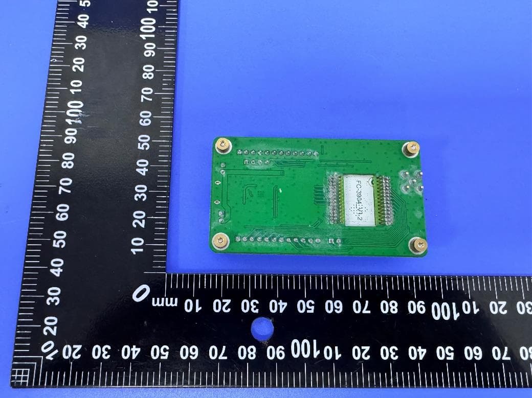
UU3FCWSL05
Mar 14, 2024LoRaWAN wireless communication model
Equipment Class
DSS - Part 15 Spread Spectrum Transmitter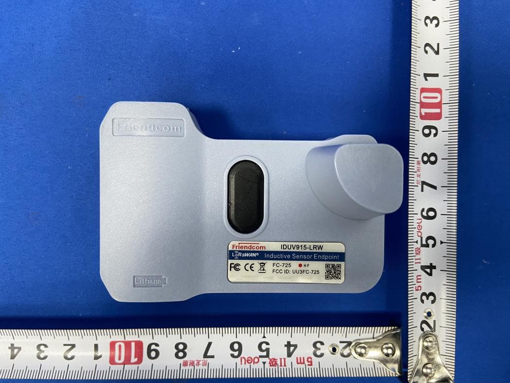
UU3FC-725
May 05, 2023IDUV915-LRW Inductive Sensor Endpoint
Equipment Class
DSS - Part 15 Spread Spectrum Transmitter
UU3FC-714
May 20, 2021Wireless Pulse Acquisition Module PULSE915-LRW
Equipment Class
JAB - Part 15 Class B Digital Device
UU3FCWSL05-A0
Apr 25, 2021LoRaWAN Module
Equipment Class
DSS - Part 15 Spread Spectrum Transmitter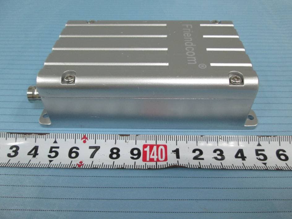
UU3FC302U2D
Jan 03, 2016FC-302 Data Radio
Equipment Class
TNB - Licensed Non-Broadcast Station Transmitter