V4FY-CAMNETWORK CAMERA
Y-CAM SOLUTIONS LTD.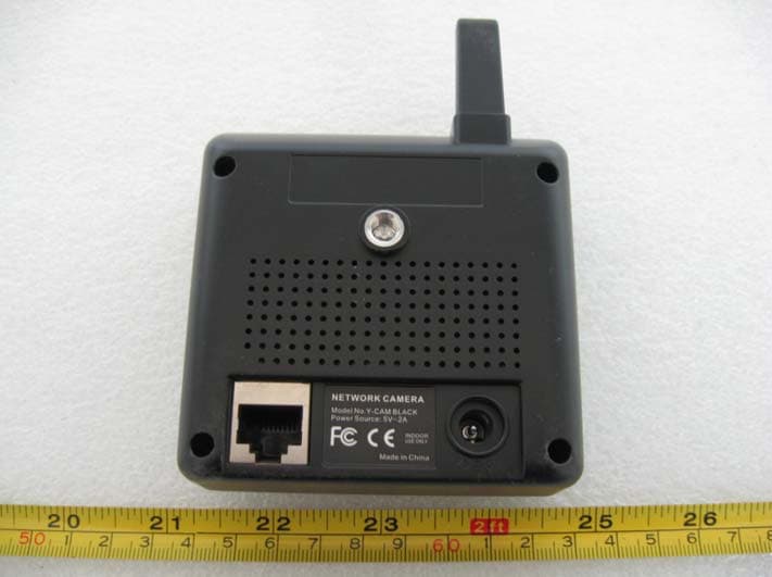
Click to zoom
Application Details
- Equipment Class
- DTS - Digital Transmission System
- Date of Grant
- Apr 01, 2008
- Application Purpose
- Original Equipment
- Date of Application
- Apr 01, 2008
- Equipment Note
- NETWORK CAMERA
- Frequency Range
- 2412.00000000 - 2462.00000000
- Company
- Y-CAM SOLUTIONS LTD.
- Country
- United Kingdom
Documents & Files
Document Text
Text extracted from the exhibit documents filed with the FCC. Open a document above to read the original.
Users Manual
User's Manual V1.01 Wireless Network Camera MODEL: IP207W Please read this manual carefully before you attempt to install this product and retain it for your future reference. 1 INTRODUCTION Thank you for your interest and support in our product and purchasing this wireless network camera IP207W. IP207W can be accessed remotely, and controlled from any PC/laptop over the Intranet or Internet via web browser. The user-friendly installation procedure and intuitive web-based interface offer easy integration with your LAN environment or WiFi system. IP207W also comes with a lot of useful alarm tool for notice user any situation. We feel confident that you will be pleased with the quality and features of this product. Notice This product may cause interferences with other wireless equipment that operates at 2.4GHz ISM band. Please turn off one of the equipments to eliminate the interference. Product Assurance This camera will emit electromagnetic wave, just like other wireless products, but its transmitting power is less than other wireless products such as mobile phones. The 2.4GHz wireless camera meets wireless frequency security standards and recommended indexes while working. These standards and indexes are certificated by academic organization and represent the cogitative research of the scientific workers who continuously explore and annotate the involved fields. So we believe that our products are safe for customers. Approval Information All our products meet the requirements of approval FCC or CE, and are granted the FCC or CE certification. They are authorized to bear FCC or CE mark. FCC WARNING: FCC Radiation Exposure Statement: This equipment complies with FCC radiation exposure limits set forth for an uncontrolled environment.This equipment should be installed and operated with minimum distance 20cm between the radiator & your body. This transmitter must not be co-located or operating in conjunction with any other antenna or transmitter. This device complies with Part 15 of the FCC Rules. Operation is subject to the following two conditions: (1) This device may not cause harmful interference, and (2) this device must accept any interference received, including interference that may cause undesired operation Changes and modification not expressly approved by the manufacturer or registrant of this equipment can void your authority to operate this equipment under Federal Communications Commissions rules. CE This product complies with standards including Low Voltage Device Directive 73/23/EEC; EMC Directive 89/336/EEC and R&TTE Directive 1999/5/EC. It passed the subject tests by the authority concerned and is authorized to bear CE mark. 2 Restrictions 1. DO NOT use this product to violate one's privacy. Monitoring one's activities without consent is illegal and this product is not designed and manufactured for such purpose. 2. DO NOT put this product near any medical equipment. Radio waves might potentially cause breakdown of electrical medical equipment. 3. This product should be placed at least 1 foot away from any heart pacemaker. Radio waves might potentially influence heart pacemaker. 4. DO NOT use this product for any illegal activities. It is the user’s responsibility to ensure that the usage of this camera is of a legal nature. Maintenance 1. Ensure that the IP207W and its power source have sufficient ventilation; 2. Do not shake, strike or drop the product; 3. Keep the camera dry and dustless and avoid exposing it to direct sunlight; 4. Do not place the product near any magnetic objects; 5. Avoid putting the product in places where there is constant temperature and humidity change; 6. Keep the product away from heat sources; 7. Do not use the camera near aggressive chemicals; 8. Do not use this camera near water; 9. Do not use the camera in the places which are enclosed by metal. The surrounding metal may shield the electromagnetic waves, and result in failure of signal reception; 10. Please obey the local government's environment protection policy; 11. Please turn off the power when left unused; 12. Do not disassemble or attempt to repair the camera; doing so might cause damage to the product. 3 MAIN FEATURES Easy Installation The IP207W comes with built-in Wireless capability and a Web Server, therefore there is no need to install a driver. The setup CD-ROM includes the Camera Setup software, User Manual and Quick Installation Guide. With industry standard automatic configuration-UPnP(Universal Plug and Play), your PC will discover and connect to your camera automatically. Once connected, using a simple Web browser you can see what the camera sees from anywhere in the world! The IP207W can be either wall-mounted or ceiling-mounted using the supplied stand. It can also be placed on a desktop using the supplied stand, thus providing a flexible installation solution. Wireless LAN Connection Available The IP207W is designed to not only work with your existing wired network but also with standard wireless devices, allowing the flexibility to operate the IP207W wirelessly. The IP207W utilizes SSID filtering, powerful 64/128 bit WEP and new security standard WPA encryption to protect you from illegal intrusion. High-Speed MPEG4 The IP207W features MPEG 4 compression which compresses the video to make transmission -faster and more efficient. The MPEG 4 image can be transmitted with a bit rate of 2048kbps at 30 frames per second. Infrared Night Vision The camera utilizes 30 infrared LED to provide high light in darks environment. When the environment is dark, the LED will be opened automatically due to a photosensitive component, and the moving images will be changed to Black and White. Users can monitor clearly the things within 12 meters distance. Users also can select open or close the infrared LED manually, and select whether change the images to black and white or color automatically. Multi-Client Access The IP207W allows up to 16 users to view the MPEG 4 image simultaneously. …
Text truncated - open the document above for the full version.
Block Diagram
Gilbert ZCOMA Wireless Networking Company 2006.04.1 Block Diagram PLL USB 2.0 7 ZD1211B-QF BB & MAC Q ADC I ADC Q DAC I DAC TX ADC AL2230S ZIF & PA RF VCO SYNTH. LNA_H/L RX I PA_DET RX Q TX I TX Q RX BB AGC /TX_AGC MEMORY Controller FIFO LED ANT _SEL, ANT _SEL# Status LED Loop Filter DIVIDE BY TWO LPF QUAD UP/DOWN CONVERT TEST PORT RF SWITCH ANT USB 2.0 HOST LPF 2.4V LDO MAC Controller External Memory Control GPIO Baseband Processor RF Interface Power management EEPROM 3 Wire control LE, CLK,DATA GC1~7 40MHz CLOCK BALUN SPM3225 RF SWITCH
External Photos
Y-CAM SOLUTIONS LTD. MODEL: Y-CAM BLACK REPORT NO.: STR08028025I FCC PART 15.249 EXHIBIT 2 - EUT EXTERNAL PHOTOGRAPHS EUT View 1 EUT View 2 Y-CAM SOLUTIONS LTD. MODEL: Y-CAM BLACK REPORT NO.: STR08028025I FCC PART 15.249 EUT View 3 EUT View 4(Adding model: Y-CAM White)
ID Label/Location Info
Y-CAM SOLUTIONS LTD. MODEL: Y-CAM BLACK REPORT NO.: STR08028025I FCC PART 15.249 EXHIBIT 1- PRODUCT LABELING Proposed FCC ID Label Format FCC ID: V4FY-CAM This device complies with Part 15 of the FCC Rules. Operation is subject to the following two conditions: (1) this device may not cause harmful interference, and (2) this device must accept any interference received, including interference that may cause undesired operation. Specifications : Text is Black in color and justified. Labels are printed in indelible ink on permanent adhesive silk-screened onto the EUT or shall be affixed at a conspicuous location on the EUT. Proposed Label Location on EUT FCC ID Label Location
ID Label/Location Info
Y-CAM SOLUTIONS LTD. MODEL: Y-CAM BLACK REPORT NO.: STR08028025I FCC PART 15.249 EXHIBIT 1- PRODUCT LABELING Proposed FCC ID Label Format FCC ID: V4FY-CAM This device complies with Part 15 of the FCC Rules. Operation is subject to the following two conditions: (1) this device may not cause harmful interference, and (2) this device must accept any interference received, including interference that may cause undesired operation. Specifications : Text is Black in color and justified. Labels are printed in indelible ink on permanent adhesive silk-screened onto the EUT or shall be affixed at a conspicuous location on the EUT. Proposed Label Location on EUT FCC ID Label Location
Internal Photos
Y-CAM SOLUTIONS LTD. MODEL: Y-CAM BLACK REPORT NO.: STR08028025I FCC PART 15.249 EXHIBIT 3 - EUT INTERNAL PHOTOGRAPHS EUT Housing and Board View 1 EUT Housing and Board View 2 Y-CAM SOLUTIONS LTD. MODEL: Y-CAM BLACK REPORT NO.: STR08028025I FCC PART 15.249 Solder Board-Component View 1 Solder Board-Component View 2 Y-CAM SOLUTIONS LTD. MODEL: Y-CAM BLACK REPORT NO.: STR08028025I FCC PART 15.249 Solder Board-Component View 3 Solder Board-Component View 4 Y-CAM SOLUTIONS LTD. MODEL: Y-CAM BLACK REPORT NO.: STR08028025I FCC PART 15.249 Solder Board-Component View 5 Solder Board-Component View 6 Y-CAM SOLUTIONS LTD. MODEL: Y-CAM BLACK REPORT NO.: STR08028025I FCC PART 15.249 Solder Board-Component View 7 Solder Board-Component View 8 Y-CAM SOLUTIONS LTD. MODEL: Y-CAM BLACK REPORT NO.: STR08028025I FCC PART 15.249 Solder Board-Component View 9
Operational Description
Circuit Description For OT207OV77201VB 1.The J1 is used to connect OT207OV77201VB to OT2067FIC81201VB.OT2067FIC81201VB provide 3.3V power supply to OT207OV77201VB and OT207OV77201VB output CCIR656 signal to OT2067FIC81201VB. 2.The resistor R1,R2,R3,R4,R5,R6,R7,R8,R9,R10 are series terminal for CCIR656 signal . 3. R11 and C7 are RC power on reset circuit for U2. 4. U1 is a LDO and output 2.8V to the DOVDD of U2. C1 is decoupling capacitors for DOVDD pin of U2. L4,C13 and C14 is filter network for DOVDD pin of U2. L2,C11 and C12 is filter network for AVDD pin of U2. 5. Q1 is a LDO and output 1.8V to supply the digital core of U2. L4,C13 and C14 is filter network for DOVDD pin of U2. 6. U2 is a CMOS sensor . U2 capture the image and sent out CCIR656 signal to DSP.C5 and C6 are decoupling capacitors for reference voltage pin of U2. 7. Y1 is a 24MHz Oscillator and provide clock sourse to PLL of U2. Circuit Description For OT207IRLED1VB 1. The J1 is used to connect OT207IRLED1VB to OT2067FIC81201VB.OT2067FIC81201VB provide 5.0V power supply to OT207IRLED1VB and OT2067FIC81201VB give a IR_ON signal to OT207IRLED1VB for control the power of IR LED. The IR_ON signal is Active HIGH. 2. OT207IRLED1VB general CDS_IN signal to OT2067FIC81201VB while the light of environment is dark,the CDS_IN signal is Active HIGH. 3. The Q1 and U1 are control circuit for power of IR LED. When the IR_ON is coming ,the Q1 is become saturation and the the pin number 4 of U1 is High. The U1 will be ON ,then IR LED get 5V power from OT2067FIC81201VB. 4. R1 is a CDS. Q3 and Q5 are P-Channel Enhancement Mode Field Effect Transistor.Q2 and Q4 are Micro-Power Voltage Detectors. The threshold of Q2 and Q4 are 2.93V. While the light of environment is dark,the resistence of R1 become to 1M ohm.At this time the Q3 and Q5 will be ON,then voltage of the Q2 and Q4 's pin 3 is larger than 2.93V. The Q2 and Q4 output HIGH. 5. The AL-513IR-850-45C are Infrared LED lamps. Circuit Description For OT2067FIC81201VB 1. Power supply The whole power source is from a 5V/2A power adapter through J7. D2 is a Transient Voltage Suppressor for 5V power supply. L8 is a EMI Suppression Filters. C85 and C86 are filter for 5V power supply. U9 is a DC-DC converter for system power supply. Switching frequency of U9 is 1.25 MHz and output 3.3V/1.2 A. U12 is a DC-DC converter for digital core power of U3 . U12 is 1 MHz fixed frequency PWM operation and output 1.8V/300mA. 2. MPU U3 is an integrated System-on-a-Chip platform for the application of the multimedia processing system.The FIC8120 is equipped with a media Codec to accelerate video processing and a comprehensive set of system and peripheral functions to be useful in a variety of multimedia processing applications. Y3 is a Crystal resonator of 22.1184MHz for PLL clock of U3 . Y1 is a Crystal resonator of 30MHz for USB PHY clock of U3 .R1 is reference resistor for USB HOST. Q3 is a Reset IC for system. C8,C64,C67,C68 are bypass Capacitor for PLL1 and PLL2 of U3. J4 and J10 is double PCB layout and they are USB2.0 HOST interface for USB.J4 and J10 connect a USB wireless WLAN module with a calbe in this design. J5 is used to connect OT2067FIC81201VB to OT207OV77201VB .OT2067FIC81201VB provide 3.3V power supply to OT207OV77201VB and OT207OV77201VB output CCIR656 signal to OT2067FIC81201VB.U3 sets the register value of U2 on OT207OV77201VB through I2C bus. J3 is GPIO function and is used to connect OT207IRLED1VB to OT2067FIC81201VB. OT2067FIC81201VB provide 5.0V power supply to OT207IRLED1VB and control the power of IR LED. The IR_ON signal is Active HIGH. J2 is JTAG interface for debug U3. 3. Audio, RTC U1 is an AudioCODEC. U10 is an Audio Amplifier. MIC1 is an Electret condenser microphone. The Audio signal is amplified and sent to U1 which converses it to digital signal. Through I2S interface, the digital signal is sent to U3. U3 sets the register value of U1 through I2C bus. U8 is a realtime clock IC. BT1 is a Li-battery. When the system is out of power, BT1 can supply the power to U8. U3 sets the register value of U8 through I2C bus. U3 reads the system time and date from U8. Q1, Q2 and R22 compose the charging circuit for BT1. 4.Network U7 is an Ethernet PHY and connects U3 through MII interface and U3 has a MAC to control PHY. Y2 is a Crystal resonator of 25MHz for PLL clock of U7. U13 is a transformer for network. J6 is RJ45 connector. C18 and C75 is decoupling capacitors for DVDD of U7. R22, R25, R26 & C84 compose pop smith circuit for EMI issue. L5 and C22 is filter network for AVDD pin of U7. 5.Memory U4 and U11 is SDRAM for ARM and DSP. U2 is NOR FLASH for saving Firmware and system seting. 6.Other U5 is a EEPROM whitch used to save the MAC adress and other system seting for product.
Schematics
55 44 33 22 11 D D C C B B A A OSCILLATOR CIRCUIT FOR MAC/ RF Open: Normal operationShort: Installation(default at factory) POWER SUPPLY CIRCUIT ShieldcaseCover: 65-003001-31NFrame: 65-020001-48NPCB70-A07602-20N FiducialMark ZCOM XG-760N IEEE802.11G USB Dongle 2.0 802.11G Zyas ZD1211B MAC/BBP Circuitry C 11 Tuesday, April 18, 2006 TitleSize Document Number Rev Date: Sheet of MA20 GC2 V3.3_BUCK MD3 V1.8D USB_DM D- MA14 USB_D- GNDD MA5 GNDD MA9MD2 V3.3 GND_USB MA0 LINKGNDD GNDA GNDD GC3GND_USB MD5 RPU MA6 MA13 MA21 SHDN# GNDD TXI+ MD[0-7] USB_DP MA5 TR_SEL# ICE_SCK SYNDATA MA17 GNDD FLSH_WP# MD0MD6 TX_VGC ICE_EN MA4MA19 GC5 SEN GPIO1 MA0 MA15 GC6 SCLK MCLK MCE# FWE# V1.8D VRPVRN V3.3 GNDA MA16 SYNCLKMA10 MD3 GNDDGNDD VCM MA1 GND_USB MA13 V3.3 FLSH_RY MD4 MD6 TXQ+ V1.8D TX_AGC_IN2 SYNCLK MA16 V3.3_reg1 MCLK 12MCLKO MA8 TXI- MD7 MA17 SYNDATA MA11 GPIO1 SENV3.3A_USBGC7VUSB5V MA9MA8 MD2 V1.8D PDNMCLK TR_SW_EXTRA GC4 MA11 ADC3-VREF-H V3.3A_USB MA2 GNDA TX_AGC_IN1 GNDD MA12 MD0 MA18 GC1 TRAFFIC MD1 MWE# V3.3 CLKINRF MA20 GC2 V2.8A_OSC MD7 MA7 GNDDV3.3 V3.3EXTRES USB_D+ ICE_SD FA0 RREF TR_SEL MA10 MA1 MD1 PDNMCLK_R TXQ- VBGCAP12MCLKO MA3 MA14 V3.3_reg2 MA7 V1.8D MA3 FA0 GNDA GNDD MA12 ADC3-VREF-F MOE# PDNMCLK MA19 GC5 MA18 GC1 V3.3A MA21 SHDN# MWE# V1.8D FLSH_RST# V3.3A RXHP SDO MA15 GC6 RX_VGC MA2 GNDDGNDD MA4 40MHZ_OUT PA_PE1 V3.3 MD4 MA6 MD5 FWE# LED1-LED2- UART_TXDUART_RXD MODE0 D+ VCC_USB GC1 PA_PE1 TXQ+ TR_SEL RX_VGCTX_VGC TXI-RXI- GC4 TX_AGC_IN1 RXQ- GC6 TXI+RXI+ GC3 GC7 SHDN# CLKINRF RXQ+ GC2GC5 SYNCLK RXHP TR_SEL# TXQ- SYNDATASEN V3.3 V3.3A_USB V3.3 V3.3 V3.3 V3.3 V3.3A V3.3A V3.3 V2.8A V2.8A V3.3 V1.8D VUSB5V VPA_3.3V V1.8D V3.3A_USB V3.3A VUSB5V V3.3 V3.3 V3.3 V3.3 C2100nF 12 C20100nF 1 2 NOP 0RR19 12 3K3R R9 1 2 C8712pF 12 H4 NOP 10KR R4 1 2 C244u7F/X5RC0805N 12 C41 100nF 1 2 C344u7F/X5RC0805N 12 ShortR16 1 2 C31100nF 1 2 NOP 220RR30 1 2 C6100nF 1 2 C26NOP 100nF 12 J2NOP CON_ACES88266-041110 1234 56 VD-D+G GG C10 1UF 1 2 C7 4u7F/X5RC0805N 12 220RR47 1 2 C9 26K7R 1 2 L40RL0402 1 2 1KRR57 12 C13 1UF 1 2 U7RT9167-28PB 31 45 2 SHDNIN BP OUT GND NOP 10KRR29 1 2 C43 100nF 1 2 C44 100nF 1 2 L110R L0402 1 2 0R R8 1 2 C25100nF 1 2 300RR27 12 R15 26K7R NOP 10KR R6 1 2 L30RL0402 1 2 NOP 430R_1% R17 1 2 C4NOP 100nF 1 2 47RR45 1 2 U8AT24C32 59-102002-06NTSSOP-8 1234 5678 A0A1A2GND SDA SCL WP VCC C84u7F/X5RC0805N 12 U2NOP AM29LV320MB_TSOP 25 24232221201918 87654321 48 1716 9 10 29313335384042443032343639414345462737 1311121415 472628 A0 A1A2A3A4A5A6A7A8A9A10A11A12A13A14A15 A16 A17A18A19A20 D0D1D2D3D4D5D6D7D8D9 D10D11D12D13D14 D15/A-1 VSSVSS VCC NCWE#RESET#WP#/ACCRY/BY# BYTE# CE# OE# C14u7F/X5RC0805N 12 C32100nF 1 2 NOPR13 12 U5RT9167-18PB 31 45 2 SHDNIN BP OUT GND 0R R5 1 2 J1 USBA Male Connector USBA_M_SMT 4321 7 65 8 5V D- D+ G G GG G NOP 10KR R7 1 2 NOP 44K2R_1%R58 1 2 0R R21 1 2 C27100nF 1 2 0R R10 1 2 C474u7F/X5RC0805N 1 2 L5Short 1 2 D2GREEN 1 2 499RR31 12 C22NOP 12 NOP 0RR20 12 C40 100nF 1 2 H4 U6 NOP MC74HC1G32 132 54 U9 OSC 5X3.2 40MHZ eCERAOSC5X3 12 34 NCGND OUT VCC C35100nF 12 C45 100nF 1 2 U1RT9166A-33PXLSOT-89 1 3 42 G O II 0R R11 1 2 C38100nF 1 2 NOP 1K5RR42R0402 1 2 10KRR35 12 H1 C46 100nF 1 2 C28100nF 1 2 100KRR3 12 C48NOP 100nF 12 C374u7F/X5RC0805N 12 D3GREEN 1 2 C23100nF 12 C33100nF 1 2 C5100nF 12 C12100nF 12 C42 100nF 1 2 C36100nF 12 300RR25 12 C11 1UF 1 2 499RR32 12 H2 12K1R_1%R43R0402 1 2 0R R12 1 2 USB General +1.8V RF Digital I/F Host InterfaceGeneral AD/DA +3.3V AD/DAUSB +3.3V General +3.3v U3 ZD1211B-QFQFP128/16/0.4 2 106 78 105 81838079 104103102101100 9998977782848586878889909192 115114 223756577494 111 213855587595 112 4544 116117 1936507393 110 2048547696 113 51524953 107108109 4746 596463676872616570343231304235412926232428274039124332543127119120121122101115141128678451261312312562663916118606971181712 RX_VGC R/B_NFALEFCLEXITR3XITR2XITR1XITR0FWPONFWPINSGPIO5SGPIO4SGPIO3SGPIO2SGPIO1SGPIO0FWE_NFRE_NFCE_NFD7FD6FD5FD4FD3FD2FD1FD0LED1LED0VDDIVDDIVDDIVDDIVDDIVDDIVDDIGNDIGNDIGNDIGNDIGNDIGNDIGNDIEESCKEESDAMODE0MODE1VDDPVDDPVDDPVDDPVDDPVDDPGNDPGNDPGNDPGNDPGNDPGNDP40MCLKIPDN40MRSTSW12MCLKOICE_SCKICE_SDICE_ENURTXDURRXD XSCI DP DM DMRS DPRS VBUS GNDAGNDAGNDA B6 SEN SCLK SDATA B1B5B2 SHDNB TR_SW_N ANTSEL ANTSEL_N PA_PE1PA_PE2 B3 B4/TR_SW_EXTRA TX_VGC B7/LNAGS TR_SW RXHP/TR_SW_EXTRA_N VREF2 TXQ_N TXQ_P TXI_P TXI_N RXI_P RXI_N RXQ_P RXQ_N TX_AGC_IN2TX_AGC_IN1 VCM VRN VRP EXTRES VBGCAP VREF AVDDAVDDAVDD RREF RPU AGNDAGNDAGNDAGND VDDAVDDAVDDA ADVDD ADGND AVDD 100KRR2 12 220RR34 1 2 C29100nF 1 2 NOP 200KR_1%R59 1 2 300RR46 1 2 L1NOP 4.7uH 20% 3.85×3.85mmELL4LM NOP 10KRR23 1 2 L120R L0402 1 2 L20RL0402 1 2 0R R14 1 2 220RR28 1 2 U12NOP MPS1556 123 45 EN GND SW VINFB NOP 0R R22 1 2 C30100nF 1 2 H3 R1NOP 499R C34u7F/X5RC0805N 12 10RR44 1 2 C14100nF C0402 12 10KR R18 1 2 L6MLB-201209-0030A-N1L0805N 1 2 C214u7F/X5RC0805N 12 300RR26 12 300RR24 12 H4 U4 NOP MC74HC1G32 132 54 55 44 33 22 11 D D C C B B A A CON1 NOPNOP C62 L13C16 -> 7pFCON1 POPC62-> 7PF L13->TOKO 6n8HNOP C16 TR_SW# TR_SW ZCOM XG-760N IEEE802.11G USB Dongle 2.0 802.11G Airoha AL2230S Front End Circuitry C 11 Tuesday, April 18, 2006 TitleSize Document Number Rev Date: Sheet of TX_PA CLKINRF BALIN_P CLKIN_RF GC3 RX_ON V2.8A GC1 PA_PE1GC6 RBIAS VPA_3.3V SYNCLK V2.8A BPF1 GC5GC2 VPA_3.3V VPA_3.3V V2.8A PAO_P BALIN_N V2.8A CP RXHP SEN GC7 SYNDATA V2.8A SHDN# LNAIN GC4 V2.8A CP_RC V2.8A V2.8A_PLL PAO_N ANT REGCAP_2.4V UFL_1 N BAL_OUT RXQ- 2 SHDN# 2 TXQ+ 2 TXI- 2 SYNCLK 2 RXI+ 2 GC6 2 TXQ- 2 GC7 2 SYNCLK 2 GC5 2 SEN 2 RXQ+ 2 CLKINRF 2 GC4 2 GC2 2 TXI+ 2 GC3 2 GC1 2 TR_SEL# 2 TX_AGC_IN1 2 SYNDATA 2 RXHP 2 RXI- 2 SYNDATA 2 PA_PE1 2 TR_SEL 2 GNDD V2.8A V2.8A REGCAP VPA_3.3V V2.8A C7910nF 12 ANT 2412-2462MHz 1 C557pF 1 2 CON1U.FL-LP-040 1 23 C717pF 1 2 NOP R51 1 2 L9 2n2H 1 2 .S314 U11HWS408HWS408 321 654 OUT1 GND OUT2 VC2RF_INVC1 C68NOP 12 C813p3F 12 L102n2H 1 2 0R R33 1 2 L8 2n2H 1 2 C394u7F/X5RC0805N 12 C62NOP 7pF 1 2 C767pF 12 ShortR56 1 2 C5222nF 12 C6522nF 12 C547pF 12 C77100nF 12 L7NOP 1n8H 12 L13NOP 6n8H 12 C844u7F/X5R 12 C757pF 12…
Text truncated - open the document above for the full version.
Test Report
Y-CAM SOLUTIONS LTD. MODEL: Y-CAM BLACK Report No.: STR08028025I-1 Page 1 of 30 FCC PART 15.247 FCC Part 15C Measurement and Test Report For Y-cam Solutions Ltd 3 Dee Road, Richmond, Surrey, TW9 2JN, United Kingdom FCC ID: V4FY-CAM Report Concerns: Original Report Equipment Type: Network Camera Model: Y-CAM Black Report No.: STR08028025I-1 Test/Witness Engineer: Test Date: 2008-02-19 to 2008-02-29 Prepared By: Shenzhen SEM.Test Compliance Service Co., Ltd 3/F, Jinbao Commerce Building, Xin'an Fanshen Road, Bao'an District, Shenzhen, P.R.C.(518101) Approved & Authorized By: Jandy So / PSQ Manager Note: This test report is limited to the above client company and the product model only. It may not be duplicated without prior permitted by SEM.Test Compliance Service Co., Ltd . Y-CAM SOLUTIONS LTD. MODEL: Y-CAM BLACK Report No.: STR08028025I-1 Page 2 of 30 FCC PART 15.247 TABLE OF CONTENTS 1. GENERAL INFORMATION ...................................................................................................................................3 1.1 PRODUCT DESCRIPTION FOR EQUIPMENT UNDER TEST (EUT)...............................................................................3 1.2 TEST STANDARDS...................................................................................................................................................3 1.3 RELATED SUBMITTAL(S)/GRANT(S) .......................................................................................................................3 1.4 TEST METHODOLOGY.............................................................................................................................................4 1.5 TEST FACILITY.......................................................................................................................................................4 1.6 EUT EXERCISE SOFTWARE....................................................................................................................................4 1.7 ACCESSORIES EQUIPMENT LIST AND DETAILS.......................................................................................................4 1.8 EUT CABLE LIST AND DETAILS.............................................................................................................................4 2. SUMMARY OF TEST RESULTS ...........................................................................................................................5 3. §15.203 - ANTENNA REQUIREMENT..................................................................................................................6 3.1 STANDARD APPLICABLE.........................................................................................................................................6 3.2 TEST RESULT..........................................................................................................................................................6 4. CONDUCTED EMISSIONS ....................................................................................................................................7 4.1 MEASUREMENT UNCERTAINTY..............................................................................................................................7 4.2 TEST EQUIPMENT LIST AND DETAILS.....................................................................................................................7 4.3 TEST PROCEDURE...................................................................................................................................................7 4.4 BASIC TEST SETUP BLOCK DIAGRAM.....................................................................................................................7 4.5 ENVIRONMENTAL CONDITIONS..............................................................................................................................8 4.6 SUMMARY OF TEST RESULTS/PLOTS......................................................................................................................8 4.7 CONDUCTED EMISSIONS TEST DATA......................................................................................................................8 5. POWER SPECTRAL DENSITY ...........................................................................................................................11 5.1 STANDARD APPLICABLE.......................................................................................................................................11 5.2 TEST EQUIPMENT LIST AND DETAILS...................................................................................................................11 5.3 TEST PROCEDURE.................................................................................................................................................11 5.4 ENVIRONMENTAL CONDITIONS............................................................................................................................11 5.5 SUMMARY OF TEST RESULTS/PLOTS....................................................................................................................12 6. 6-DB BANDWIDTH ................................................................................................................................................16 6.1 STANDARD APPLICABLE.......................................................................................................................................16 6.2 TEST EQUIPMENT LIST AND DETAILS...................................................................................................................16 6.3 TEST PROCEDURE.................................................................................................................................................16 6.4 ENVIRONMENTAL CONDITIONS............................................................................................................................16 6.5 SUMMARY OF TEST RESULTS/PLOTS........................................…
Text truncated - open the document above for the full version.
Test Setup Photos
Y-CAM SOLUTIONS LTD. MODEL: Y-CAM BLACK REPORT NO.: STR08028025I FCC PART 15.249 EXHIBIT 4 - TEST SETUP PHOTOGRAPHS Conduction Emission Test Setup Radiation Emission Test Setup (30MHz to 1GHz) Y-CAM SOLUTIONS LTD. MODEL: Y-CAM BLACK REPORT NO.: STR08028025I FCC PART 15.249 Radiation Emission Test Setup (Above 1GHz)
Contact Information
Applicant
SHENG TANG(OPERATIONS DIRECTOR)
Test Firm
Solid Industrial Co., Ltd.Yang Dengfang
Technical Specifications
| # | Rule Parts | Frequency Range | Power Output |
|---|---|---|---|
| 1 | 15C | 2.41 GHz - 2.46 GHz | 89.90 mW |
Other Applications from Y-CAM SOLUTIONS LTD.

V4FCUBEHD720
Mar 06, 2013Y-cam Cube
Equipment Class
DTS - Digital Transmission System
V4FCUBE
Mar 05, 2013Y-cam Cube
Equipment Class
DTS - Digital Transmission System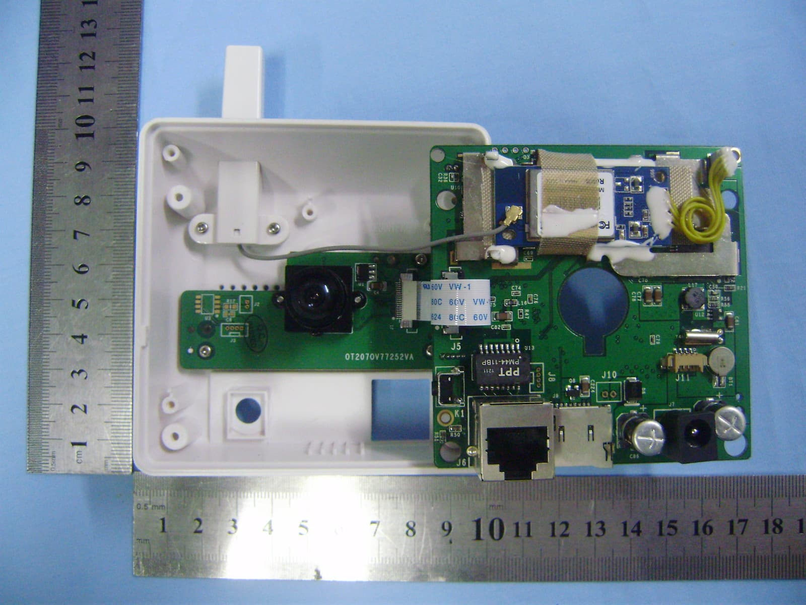
V4FYCK020
Dec 18, 2012NETWORK CAMERA
Equipment Class
DTS - Digital Transmission System
V4FBABYV026
Dec 17, 2012NETWORK CAMERA
Equipment Class
DTS - Digital Transmission System
V4FYCHME61
Dec 17, 2012NETWORK CAMERA
Equipment Class
DTS - Digital Transmission System