V65K009CDMA Phone
Kyocera Corporation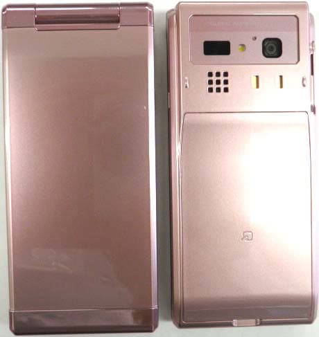
Click to zoom
Application Details
- Equipment Class
- DSS - Part 15 Spread Spectrum Transmitter
- Date of Grant
- Mar 24, 2011
- Application Purpose
- Original Equipment
- Date of Application
- Mar 24, 2011
- Equipment Note
- CDMA Phone
- Frequency Range
- 2402.00000000 - 2480.00000000
- Company
- Kyocera Corporation
- Country
- United States
Documents & Files
Document Text
Text extracted from the exhibit documents filed with the FCC. Open a document above to read the original.
Users Manual
Operating Instructions Name & Function of Parts 17 TV key 1 Earpiece 18 Built-in antenna (for Bluetooth) 2 Main Display 19 Built-in antenna (Sub antenna) 3 Optical sensor 20 LED Display 4 OK key 21 Illumination 5 Address book key 22 Infrared port 6 Mail key 23 Speaker 7 Clear /News key 24 Battery pack/cover 8 Answer/Pair key 25 FeliCa mark 9 Number keys 26 Camera lens 10 Self Menu key 27 Flash/Camera start indicator 11 Microphone 28 Charging terminals 12 Built-in antenna (Main antenna) 29 Manner key 13 Cursor key 30 External connection jack/cover 14 Application key 31 Strap hole 15 EZ key 16 Power/End key - 1 - ■ Power saving during standby In order to minimize the power consumption, the K009 display turns automatically to power saving mode when key operation is stopped for a while. The indication restores with key operation. ■ a key In this manual, the point at which to press the a key is indicated as shown below. Example) Press u or d → j Getting Ready to Make a Call 1. Charging with the AC Adapter The battery charger can be charged by directly inserting the AC Adapter connector into the external connection terminal on the K009 Main Unit. 2. Turning the power on Press and hold N or more than one second. ◆Turning the power off Press and hold F for more than one second. Switch to English 1. Press c on the standby screen. 2. Select "機能設定" and press c (選択). 3. Press 35 . 4. Select "English" and press c (Set). Displaying your own phone number 1. Press c on the standby screen. 2. Press 0 to display your au telephone number. Making a Call 1. Enter the phone number you want to call on the standby screen. Area code - Local code - Subscriber's number. <Example> 03-0001-XXXX Always include the area code, even when calling to a number in the same area you are in. If you enter a wrong number: ● Press C briefly - the last dialed digit will be deleted. ● Press and hold C - the entire phone number will be deleted. 2. Press N to make a call. - 2 - Making an International Call 1. Enter the phone number you want to call using the following pattern on the standby screen. International dial code - Country code - Area code - Subscriber's number 2. Press N to make a call. <Example> to call United States, number 212-123-XXXX in the USA. Operation Explanation 1 Pressing "005345" Access code 2 Pressing "1" Country code of United States: 1 3 Pressing "212" Area code ※ : 212 4 Pressing "123-XXXX" Subscriber's number: 123-XXXX 5 Press N The following operation is the same as the normal telephone operation. ※ When the first number of the area code is "0", press the area code number without "0". Adjusting the receiver volume 1. During a call, press j . u : Volume level raised. d : Volume level lowered. Answering a call 1. The ringer tone sounds/vibrator buzzes, and the incoming call lamp flashes. 2. Press N to answer the call. An incoming call can also be answered by pressing any of the 0~9,* ,# ,L,R, s keys. If you do not answer the call or the caller disconnects before the call is answered, " Missed Call X" will be displayed. (A number appears in the "X".) Entering characters This is the method of entering names for registering address book and writing mail. 1. Press & (Char.Type). 2. Select the entry mode you want. 漢字 "Kanji", "Hiragana" entry mode (full size) 1234 "Number" entry mode (half size) カナ "Katakana" entry mode (full size) "Pictographs" entry mode カタカナ "Katakana" entry mode (half size) Sym "Symbol" entry mode AB・ab "Alphanumeric" entry mode (full size) Face "Face marks" entry mode 12 "Number" entry mode (full size) ABCD・ abcd "Alphanumeric" entry mode (half size) - 3 - [Assignment of characters and key functions] Characters are assigned to each key as shown below. Press a key repeatedly to cycle through characters assigned to that key. Entry mode key Kanji・Hiragana 漢字 Katakana カナ・カタカナ Alphanumeric AB・ABCD Alphanumeric ab・abcd Number 12・1234 1 あいうえおぁぃぅぇぉ アイウエオァィゥェォ . @ - _ / : ~ 1 . @ - _ / : ~ 1 1 2 かきくけこ カキクケコ ABC2 abc2 2 3 さしすせそ サシスセソ DEF3 def3 3 4 たちつてとっ タチツテトッ GHI4 ghi4 4 5 なにぬねの ナニヌネノ JKL5 jkl5 5 6 はひふへほ ハヒフヘホ MNO6 mno6 6 7 まみむめも マミムメモ PQRS7 pqrs7 7 8 やゆよゃゅょ ヤユヨャュョ TUV8 tuv8 8 9 らりるれろ ラリルレロ WXYZ9 wxyz9 9 [カナ]ワヲンヮ、。ー -・.!?(space)0 [AB] [ab] 0(space)! ? ・ , ’ ”_ .- 0 わをんゎ、。-・~!? (space) [カタカナ] ワヲン、。ー -・.!?(space)0 [ABCD] [abcd] 0(space) ! " #$%& ' ( )* + , - . / : ; <=>?@[¥]^_` { | } ~ 0 (before confirm) ゙ (Voiced Sound symbol) ゚(Semi-voiced Sound symbol) Switches lowercase/uppercase (before confirm) Switches lowercase/uppercase * (after confirm) 、。-・~!?(スペース) (after confirm) . , - ! ? . (before confirm)Reverse toggle of entered characters # (after confirm)line change line change Remarks: ■ “~”can be inputted only when inputting full-sized characters. It changes to“ ~”when inputting half-sized characters. ■ It is not likely to be able to change line on the input of part of character screen. ■ Inputting voiced sound symbol/semi-voiced sound symbol or switching uppercase/lowercase can be done by pressing #after inputting the character. (A list of Pictographs, Face marks, and Characters is displayed if you press it after the inputted character is set.) < Example >つ→っ→づ→つ ハ→バ→パ→ハ a→A→a - 4 - Registering in the Address Book You can register frequently used phone numbers and E-mail addresses. Up to 1000 addresses can be registered in the address book. ■ Registering in the address book 1. Press and hold & for more than one second on the standby screen. The screen to register a contact is displayed. 2. Enter the item you want. Select the icon of the item you want by j and press c (Select) to enter it. As for the items you can enter, see "Items to register in the address book". 3. Press % (Reg) . ■ Items to register in the address book The following data can be put in the address book. Name Up to 12 full size (24 half size) characters. Reading Up to 24 half size characters. Registered automatically after "Name" is entered. Phone No.1~3 Up to 32 digits. Selecting from 7 Phone number types. E-mail Address 1~3 U…
Text truncated - open the document above for the full version.
Attestation Statements
an Diego, CA 9212 KYOCERA Corporation Proprietary/Confidential DATE: 3/14/2011 Federal Communications Commission Equipment Authorization branch 7435 Oakland Mills Road Columbia, MD 21046 Subject: 13.56MHz in Kyocera FCC ID: V65K 00 9 In reference to the application under FCC ID : V65K009, KYOCERA Corporation attests that that the included device is a 13.56 MHz passive RFID device with no internal power source and no power provided by the handset. - That the 13.56 MHz device will have no capability to transmit on it's own or by control signals within the handset. - That the 13.56 MHz device operates only when in proximity (Maximum 3.94 inches) of a reader device. - That the 13.56 MHz device does not have the capability to operate as a reader. Sincerely, ____________________________ C. K. Li Director, Design Center Kyocera Corporation c/o Kyocera Communications, Inc. (KCI) 8611 Balboa Avenue, San Diego, CA 92123
Block Diagram
Tx PLLTx VCO Quadrature Up Converter Lo generation & Distribution TX_ VCON T Gain Ctl Circuits TX_O N TX_ Q TX_I TX_I Quadrature Up Converter Loop Filter RX0_IP Transceiver IC RTR-6500-O-68MQFN-TR-02 Qualcomm CDMA VCOs TCXO D i g i t a l I / O s & C o n t r o l s SSB PLL0 Quadrature Down Converter Lo generation & Distribution LPF RX0_I RX0_QP RX0_Q M RX1_IP RX1_IM RX1_Q RX1_QM Lo generation & Distribution Diversity Rx VCO Diversity Rx VCO TCX O Quadrature Down Converter LPF LPF Controls GPS CDMA VCO VDDM JDET_INT CONFIDENTIAL K009 CDMA BLOCK DIAGRAM Quadrature Down Converter Jammer detect TCXO(19.2MHz) KYH3042E NDK EXT_AN T/ BC3_DUP SAYEV856MAD0F00 MURATA Loop Filter BAND_SW UPG2012TK-E2 NEC BC6_DUP WXA08A2120FF NDK BC0_DUP EFSD836MJ2K2 Panasonic TX RX BC0/BC6_Dual PA ACPM-7351 AVAGO 2G_RFSAW SF14- 1930M5UU34 TX RX TX RX PLL1 Loop Filter LPF ANT SW CXG1215UR-T9 sony ANT SW UPG2012TK-E2 NEC 800M_BC3_Isolater CEG2391MDCB000RB5 Murata SUB/GPS_ANT 800M_BC0_Isolater CEG23836MDCB000RB5 Murata BC3_PA ACPM-7822 AVAGO TX_OUT_HB_A TX_OUT_LB_A TX_OUT_LB_B TX_OUT_HB_B GPS RF SAW SF14- 1575M5UU19 Kyocera BC3 RF SAW SF14- 0859M5UU32 BC6 RF SAW SF14- 2120M5UU31 Kyocera Power_DET_IN BAND_SW UPD5713TK-E2-A NEC BAND_SW UPD5713TK-E2-A NEC BAND_SW UPD5713TK-E2-A NEC BC3 RF SAW SF14- 0859M5UB36 BC0 RF SAW SF14- 0881M5UB34 Kyocera BC6 RF SAW SF14- 2120M5UB33 Kyocera BC0/BC3_Dual_RFSAW SF18-0836TAUU31 Kyocera RF CONNECTER MS-180 Hirose BT IC BTS-4025-0-36-W LCSP-TR-0D QUALCOMM BT_TXD BT_RXD BT_RTS UART1_CT BT_WAK BT ANT RF_TXR BT_INT BT_PCM_D I2S_PCM_DO I2S_PCM_CL I2S_PCM_LR_SYN BT_RTS SLEEP_CL VDD_A VBT VDD_I VMSMP K009 Bluetooth BLOCK DIAGRAM BT Filter FI168B245001-T TAIYO-YUDEN BT XTAL (32.0MHz) CX3225SB32000D0FLFZZ KYOCERA VDD_DVDD_P
Cover Letter(s)
KYOCERA COMMUNICATIONS, INC. 9520 Towne Centre Drive, San Diego, CA 92121 Kyocera Communications, Inc. Proprietary/Confidential Date: 2/22/2011 Federal Communications Commission Equipment Approval Services 7435 Oakland Mills Road Columbia, MD 21046 Subject: Request for Confidentiality FCC ID: V65K009 To Whom It May Concern: In accordance with §0.459 of CFR 47, KYOCERA Corporation requests confidentiality for the following items 1. Block Diagram 2. Parts List 3. Adjustment Procedure and Schematic Diagrams 4. Technical Description These items contain detailed system and equipment description and related information about the product which KYOCERA Corporation considers to be proprietary, confidential and a custom design which otherwise would not be released to the general public. Since this design is a basis from which future technological products will evolve, KYOCERA Corporation also feels that this information would be of benefit to its competitors, and that the disclosure of the information in these exhibits would give our competitors an unfair advantage in the market. Best Regards, ____________________________ C. K. Li Director, Design Center Kyocera Corporation c/o Kyocera Communications, Inc. (KCI) 8611 Balboa Avenue, San Diego, CA 92123
Cover Letter(s)
KYOCERA COMMUNICATIONS, INC. 9520 Towne Centre Drive, San Diego, CA 92121 Kyocera Communications, Inc.. Proprietary/Confidential Date: 3/11/2011 Federal Communications Commission Equipment Approval Services 7435 Oakland Mills Road Columbia, MD 21046 Subject: Request for Short-Term Confidentiality FCC ID: V65K009 To Whom It May Concern: In accordance with §0.457 and 0.459 of CFR 47, KYOCERA Corporation requests short-term confidentiality (135 days) for the following items 1. Test Setup Photos 2. External and Internal Photos 3. User’s Manual These items contain detailed system and equipment description and related information about the product which KYOCERA Corporation considers to be proprietary, confidential and a custom design which otherwise would not be released to the general public. Since this design is a basis from which future technological products will evolve, KYOCERA Corporation also feels that this information would be of benefit to its competitors, and that the disclosure of the information in these exhibits would give our competitors an unfair advantage in the market. Best Regards, ____________________________ C. K. Li Director, Design Center Kyocera Corporation c/o Kyocera Communications, Inc. (KCI) 8611 Balboa Avenue, San Diego, CA 92123
Cover Letter(s)
KYOCERA COMMUNICATIONS, INC. 10300 Campus Point Drive San Diego, CA 92121 Kyocera Communications, Inc. Proprietary/Confidential 1 of 2 Date: 6/15/2010 Federal Communications Commission c/o Compliance Certification Services Certification Division 47173 Benicia Street Fremont, CA 94538 To whom it may concern: We, the undersigned, hereby authorize the Comptest Services LLC and hereafter referred to as Comptest, to act on our behalf in all manners relating to application for equipment authorization, including signing of all documents relating to these matters. Any and all acts carried out by Comptest on our behalf shall have the same effect as acts of our own. We, the undersigned, hereby certify that we are not subject to a denial of federal benefits, that includes FCC benefits, pursuant to Section 5301 of the Anti-Drug Abuse Act of 1988, 21 U.S.C. 853(a). In authorizing Comptest as our agent, we still recognize that we are responsible to: a) comply with the relevant provisions of the certification program; b) make all necessary arrangements for the conduct of the evaluation, including provision for examining documentation and access to all areas, records (including internal audit reports) and personnel for the purposes of evaluation (e.g. testing, inspection, assessment, surveillance, reassessment) and resolution of complaints; c) make claims regarding certification only in respect of the scope for which certification has been granted; d) do not use our product certification in such a manner as to bring the Certification Division into disrepute and not make any statement regarding our product certification which the Certification Division may consider misleading or unauthorized; e) upon suspension or cancellation of certification, discontinue use of all advertising matter that contains any reference thereto and return any certification documents as required by the Certification Division; KYOCERA COMMUNICATIONS, INC. 10300 Campus Point Drive San Diego, CA 92121 Kyocera Communications, Inc. Proprietary/Confidential 2 of 2 f) use certification only to indicate the products are certified as being in conformity with specified standards; g) endeavor to ensure that no certificate or report nor any part thereof is used in a misleading manner; h) ensure that any reference to our product certification in communication media such as documents, brochures or advertising, complies with the requirements of the Certification Division; i) keep a record of all complaints made known to the us relating to the product’s compliance with requirements of the relevant standard and to make these records available to the Certification Division when requested; j) take appropriate action with respect to such complaints and any deficiencies found in products or services that affect compliance with the requirements for certification; k) document the actions taken. This authorization is valid until further written notice from the applicant. Sincerely Yours, ____________________________ C. K. Li Director, Design Center Kyocera Corporation c/o Kyocera Communications, Inc. (KCI) 10300 Campus Point Drive San Diego, CA 92121
Cover Letter(s)
Date: 7/16/10 Compliance Certification Services Certification Division 47173 Benicia Street Fremont, CA 94538, USA To whom it may concern: I, the undersigned, hereby authorize Ms. Claire Hoque/Application Examiner of Compliance Engineering Services, Inc., d.b.a. Compliance Certification Services and hereafter referred to as CCS, to act on our behalf in all manners relating to application for equipment authorization, including signing of all documents relating to these matters. Any and all acts carried out by Ms. Claire Hoque of CCS on our behalf shall have the same effect as acts of our own. I, the undersigned, hereby certify that we are not subject to a denial of federal benefits, that includes FCC benefits, pursuant to Section 5301 of the Anti-Drug Abuse Act of 1988, 21 U.S.C. 853(a). In authorizing CCS as our agent, we still recognize that we are responsible to: a) comply with the relevant provisions of the certification program; b) make all necessary arrangements for the conduct of the evaluation, including provision for examining documentation and access to all areas, records (including internal audit reports) and personnel for the purposes of evaluation (e.g. testing, inspection, assessment, surveillance, reassessment) and resolution of complaints; c) make claims regarding certification only in respect of the scope for which certification has been granted; d) do not use our product certification in such a manner as to bring the Certification Division into disrepute and not make any statement regarding our product certification which the Certification Division may consider misleading or unauthorized; e) upon suspension or cancellation of certification, discontinue use of all advertising matter that contains any reference thereto and return any certification documents as required by the Certification Division; f) use certification only to indicate the products are certified as being in conformity with specified standards; g) endeavor to ensure that no certificate or report nor any part thereof is used in a misleading manner; h) ensure that any reference to our product certification in communication media such as documents, brochures or advertising, complies with the requirements of the Certification Division; i) keep a record of all complaints made known to the us relating to the product’s compliance with requirements of the relevant standard and to make these records available to the Certification Division when requested; j) take appropriate action with respect to such complaints and any deficiencies found in products or services that affect compliance with the requirements for certification; k) document the actions taken. This authorization is valid until further written notice from the applicant. Sincerely Yours, Tina To, Account Representative CompTest Services, LLC
External Photos
Applicant:Kyocera FCC ID:V65K009 Report #:CT-K009-7-0311-R0 © 2011 Comptest Services LLC Page 1 of 2 External Photos This report shall not be reproduced except in full, without the written consent of CompTest Services LLC. EXHIBIT 7: EXTERNAL PHOTOS Applicant:Kyocera FCC ID:V65K009 Report #:CT-K009-7-0311-R0 © 2011 Comptest Services LLC Page 2 of 2 External Photos This report shall not be reproduced except in full, without the written consent of CompTest Services LLC.
Internal Photos
Applicant:Kyocera FCC ID:V65K009 Report #:CT-K009-8-0311-R0 © 2011 Comptest Services LLC Page 1 of 9 Internal Photos This report shall not be reproduced except in full, without the written consent of CompTest Services LLC. 1 EXHIBIT 8: INTERNAL PHOTOS Applicant:Kyocera FCC ID:V65K009 Report #:CT-K009-8-0311-R0 © 2011 Comptest Services LLC Page 2 of 9 Internal Photos This report shall not be reproduced except in full, without the written consent of CompTest Services LLC. Applicant:Kyocera FCC ID:V65K009 Report #:CT-K009-8-0311-R0 © 2011 Comptest Services LLC Page 3 of 9 Internal Photos This report shall not be reproduced except in full, without the written consent of CompTest Services LLC. Applicant:Kyocera FCC ID:V65K009 Report #:CT-K009-8-0311-R0 © 2011 Comptest Services LLC Page 4 of 9 Internal Photos This report shall not be reproduced except in full, without the written consent of CompTest Services LLC. Applicant:Kyocera FCC ID:V65K009 Report #:CT-K009-8-0311-R0 © 2011 Comptest Services LLC Page 4 of 9 Internal Photos This report shall not be reproduced except in full, without the written consent of CompTest Services LLC. Applicant:Kyocera FCC ID:V65K009 Report #:CT-K009-8-0311-R0 © 2011 Comptest Services LLC Page 5 of 9 Internal Photos This report shall not be reproduced except in full, without the written consent of CompTest Services LLC. Applicant:Kyocera FCC ID:V65K009 Report #:CT-K009-8-0311-R0 © 2011 Comptest Services LLC Page 5 of 9 Internal Photos This report shall not be reproduced except in full, without the written consent of CompTest Services LLC. Applicant:Kyocera FCC ID:V65K009 Report #:CT-K009-8-0311-R0 © 2011 Comptest Services LLC Page 6 of 9 Internal Photos This report shall not be reproduced except in full, without the written consent of CompTest Services LLC. Applicant:Kyocera FCC ID:V65K009 Report #:CT-K009-8-0311-R0 © 2011 Comptest Services LLC Page 7 of 9 Internal Photos This report shall not be reproduced except in full, without the written consent of CompTest Services LLC. Applicant:Kyocera FCC ID:V65K009 Report #:CT-K009-8-0311-R0 © 2011 Comptest Services LLC Page 8 of 9 Internal Photos This report shall not be reproduced except in full, without the written consent of CompTest Services LLC. Applicant:Kyocera FCC ID:V65K009 Report #:CT-K009-8-0311-R0 © 2011 Comptest Services LLC Page 9 of 9 Internal Photos This report shall not be reproduced except in full, without the written consent of CompTest Services LLC.
Operational Description
K009 EXHIBIT xx 1 /1 Technical Description of Bluetooth transmitter The Bluetooth circuit consists of a Bluetooth IC (IC1N01), filter (FL1N01), X’tal(X1N01) and antenna(AT1N01). IC0A01(QSD-8650) supplies transmitter signal to the Bluetooth IC (IC1N01)and controls the Bluetooth IC (IC1N01). The Bluetooth IC (IC1N01) internally formats the supplied data (from IC0A01) to the signal (Bluetooth format) and modulates it. The modulated Bluetooth signal from IC1N01 is input to the filter (FL1N01) by which spurious emissions are suppressed. The output signal from the filter (FL1N01) is supplied to the Bluetooth antenna and transmitted. The carrier of Bluetooth signal is generated by the PLL inside of the Bluetooth IC (IC1N01) referring to the frequency supplied by X’tal (X1N01).
Schematics
start. Rev. BOARD ETC. CIRCUIT MODEL DESIGNEDCHECKEDAPPROVED NAMECIRCUIT NO.CODE No. CONTENTS 12 11 10 9 8 7 6 QPONMLKJIHGFEDCBA 5 4 3 2 1 12 11 10 9 PAGE 8 SIGNDATENO. CIRCUIT 7 6 5 4 3 2 1 QPONMLKJIHGFEDCBA F7 F9F10 F11 F8 F4 F3 F2 F1 F6 F5 F14RF_BLOCK C0F014001Y2 11/01/05 1/19 PP1 AT0481 ANCM2859MTKC019@ FIX 3 FIX 4 FEED 1 FEED 2 5 5 6 6 IC0201 TC7SG32AFS 1 IN_A 2 GND 3 IN_B 4 OUT_Y 5 Vcc IC0106 TC7SG04AFS@ 1 INA 2 GND 3 NC 4 OUTY 5 VCC IC0104 UPD5713TK 1OUT1 2 GND 3 OUT2 4 Vcont 5 INPUT 6 VDD IC0103 UPD5713TK 1 OUT1 2 GND 3 OUT2 4 Vcont 5 INPUT 6 VDD IC0105 UPD5713TK 1OUT1 2 GND 3 OUT2 4 Vcont 5 INPUT 6 VDD IC0481 UPG2012TK-@ 1 OUT1 2 GND 3 OUT2 4 Vcont 5 INPUT 6 VDD IC0102 UPG2012TK-@ 1OUT1 2 GND 3 OUT2 4 Vcont 5 INPUT 6 VDD IC0202 74AUP1G175GM@ 1 CP 2 GND 3 D 4 Q 5 VCC 6 MR C0488 [0603] 6p C0323 [0603] 12p C0324 [0603] 33p C0337 [0603] 100p C0335 [0603] 150p C0334 [0603] 150p C0203 [0603]0.033u C0404 [0603] 56p C0326 [1005] 1u C0130 [0603] 100p C0111 [0603] 0.082u/6.3V C0141 [0603] 0.01u C0120 [0603] NU C0132 [0603] 100p C0201 [0603] 0.1u C0125 [1005] 1u C0329 [0603] 220p C0124 [0603] 0.5p C0146 [0603] 100p C0312 [0603] 33p C0110 [0603] 4700p C0139 [0603] 0.01u C0105 [0603] 100p C0151 [0603] 100p C0135 [0603] 100p C0332 [0603] 33p C0489 [0603] 2p C0131 [0603] 100p C0101 [0603] 100p C0142 [0603] 100p C0103 [0603] 100p C0409 [0603]100p C0127 [0603] 100p C0143 [1005] 1u C0149 [1005] 1u C0112 [0603] 100p C0202 [0603] 0.01u C0106 [0603] 100p C0104 [0603] 100p C0411 [0603] 100p C0150 [1005] 1u C0109 [0603] 100p C0113 [1005] 1u C0325 [0603] 0.01u C0319 [0603] 100p C0487 [0603] 100p C0129 [0603] 100p C0140 [0603] 100p C0322 [0603] 100p C0152 [0603] 0.1u C0330 [1005] 1u C0301 [0603] 0.75p 1% C0147 [0603]0.068u C0136 [0603] 100p C0117 [0603] 0.1u C0490 [0603] 8p C0491 [0603] 5p C0126 [0603] 0.01u C0328 [0603] 3300p C0308 [0603] 100p C0145 [1005] 1u C0115 [1608] 10u/6.3V C0406 [0603] 100p C0302 [0603] 0.75p 1% C0133 [0603] 100p C0407 [0603] 100p C0309 [0603] 100p C0306 [0603] 1000pC0307 [0603] 1000p C0321 [0603] 100p C0144 [1608] 10u/6.3V C0484 [0603] 100p C0481 [0603] 56p C0205 [0603] 1000p C0114 [1005] 1u C0137 [0603] 100p C0410 [0603]100p C0119 [0603] 100p C0482 [0603] 56p C0485 [0603] 33p C0483 [0603] 100p C0313 [0603] 100p C0336 [0603] 2200p C0403 [1005] 0.5p C0122 [0603] 33p C0123 [0603] 33p C0320 [0603] 100p C0304 [0603] NU C0314 [0603] 100p C0315 [0603] 100p C0493 [0603] 2p C0492 [0603] 1p C0305 [1608] 4.7u/6.3V C0352 [0603] 100p C0317 [0603] 680p C0318 [0603] 680p C0316 [1608] 4.7u/6.3V C0134 [0603] 100p C0148 [0603] 4700p C0331 [1608] 4.7u/6.3V C0402 [0603] 56p C0154 [0603] 4p C0102 [0603] 4p C0353 [0603] NU C0408 [0603] 33p C0156 [0603] 100p C0206 [0603] 0.1u C0121 [0603] 33p C0412 [1005] 10p C0153 [0603] NU C0405 [0603] 100p C0494 [1005] 1.5p NU C0474 [0603] 33p C0473 [0603] 2.2p C0470 [0603] 0.1u C0471 [0603] 33p C0472 [0603] 0.1u C0495 [1005] 1p C0138 [0603] 1.5p C0475 [0603] 33p C0420 [0603] 56p C0360 [0603] 0.3p 0.1p C0118 [0603] 100p ES0401 AVR-M1005C080MTABB [1005] FL0103 SF14-2120M5UB33 4OUT 2 GND 1IN 5 GND 3 OUT FL0101 SF14-0859M5UB36 4OUT 2 GND 1IN 5 GND 3 OUT FL0302 SF14-1930M5UU34 IN 1 2 GND 5 GND 3 GND OUT 4 GND GND IC0401 CXG1215UR 5 VDD 6 CTLA 7 CTLB 9 GND 10 RF3 11 GND 13 GND 14 RF2 15 GND 16 GND 1 RF5 2 GND 3 RF4 4 GND 8 CTLC 12 RF1 17 GND L0116 [0603] 47n(HK) L0301 [0603] 6.8n(HK) L0304 [0603] 56n(HK) L0109 [0603] 39n(HK) L0308 [0603] NU L0104 [0603] 10n(HK) L0302 [0603] 27n(HK) L0117 [0603] 10n(HK) L0118 [0603] NU L0404 [0603] 82n(HK) L0307 [0603] 10n(HK) L0489 [0603] 18n(HK) L0114 [0603] 3.9n(HK) L0311 [1005] 270n(HK) L0405 [0603] 3.3n(HK) L0495 [1005] 2.2n(HK) L0484 [0603] 12n(HK) L0488 [0603] 5.6n(HK) L0305 [0603] 27n(HK) L0108 [0603] 2.7n(HK) L0105 [0603] 82n(HK) L0487 [0603] 2.2n(HK) L0406 [0603] 8.2n(HK) L0407 [0603] 6.8n(HK) L0303 [0603] NU L0306 [0603] 10n(HK) L0107 [0603] 5.6n(HK) L0472 [0603] 4.7n(HK) L0471 [0603] 1.5n(HK) L0486 [0603] 22n(HK) L0402 [1005] 10n(HK) L0470 [0603] 22n(HK) L0312 [0603] 3.3n(HK) L0310 [1005] 270n(HK) L0309 [0603] 15n(HK) L0485 [0603] 8.2n(HK) L0115 [0603] 3.9n(HK) L0482 [0603] 82n(HK) NU L0481 [0603] 47n(HK) L0106 [0603] 3.3n(HK) L0408 [0603] 22n(HK) L0113 [0603] 47n(HK) L0120 [0603] 15n(HK) L0110 [0603] 2.7n(HK) Q0470 BFP640F 2 3 1 4 [0603] R0402 560 [0603] R0471 15K [0603] R0307 10 [0603] R0306 5.1K F [0603] R0470 12K [0603] R0305 12K F [1005] R0495 0 [0603] R0105510 F [0603] R0303 75 [0603] R0109 5.1K F [0603] R0103510 F [0603] R0108 2.2 [0603] R0354 33K [0603] R0401 10K [1005] R020456K D [0603] R0206 NU [0603] R0102 NU [0603] R0101 560 F [0603] R0351 10K [0603] R0203 2K [0603] R0304 100 [0603] R0107 47k [0603] R0202 100 [0603] R0311 47k [0603] R0312 47k [0603] R0308 47k [0603] R0310 47k [0603] R0309 47k [0603] R0403 10 [0603] R0106 47k [0603] R0472 15 [0603] R0302 100 [0603] R0201 33 [0603] R0104 5.6 [1005] R0482 0 [0603] R0404 560 [0603] R0301 51 [0603] R0353 1K SL0411 SHIELD FRAME RF SF-2411 SL0408 12 SF-2411 SL0406 12 SF-2411 SL0405 12 SF-2411 SL0402 12 SF-2411 SL0407 12 NCP15WF104F03RC SN0201 [1005] 1 2 TP_VBATT_PA0 TP_VBATT_PA X0201 KYH3042E 1 Vcon 2 GND 3 Output 4 Vcc 1122 11221122 1122 IC0302 ACPM-7822 1 Ven 2 Vmode 3 Vbp 4 RF_In 5 Vcc1 6 Vcc2 7 GND 8 RF_Out 9 GND 10 GND 11 EXT_GND IC0301 ACPM-7351-TR1 1 RFin_Cell 2 Vmode 3 Vbp 4 Vcc 5 Ven_Cell 6 Ven_IMT 7 RFin_IMT 8 RFout_IMT 15 B_GND 9 GND 10 GND 11 Vcc 12 GND 13 GND 14 RFout_Cell IC0101 IC.RTR6500-68mQFN 18 TXAGC_PDM 19 SSBI0 20 PULL_UP 21 PULL_DOWN 22 VDDM 23 SSBI1 24 DNC 25 DNC 26 JDET_INT 27 VDDRX 28 VCO_TUNE_SRX 29 VDDRX 30 VDDRX 31 RX1_IM 38 VDDRX 39 RX_IN_LB_1 40 RX_IN_HB_1 41 DNC 42 MIX_INP_LB_0 43 MIX_INM_LB_0 44 VDDRX 45 MIX_INP_HB_0 46 MIX_INM_HB_0 47 VDDRX 48 VDDRX 49 LNA_OUT_HB_0 50 LNA_OUT_LB_0 51 RBIAS_2 55 RX0_IP 56 RX0_IM 57 RX0_QP 58 RX0_QM 59 VDDRX 60 VCO_TUNE_PRX 61 VDDRX 62 TCXO 63 PWR_DET_IN 64 VDDTX 65 TX_OUT_HB_B 66 PA_R1 67 TX_OUT_HB_A 68 VDDTX 1 TX_OUT_LB_B 2 PA_R0 3 TX_OUT_LB_A 4 VDDTX 5 VDDTX 6 DAC_REF 7 TX_QP 8 TX_QM 9 TX_IP 10 TX_IM …
Text truncated - open the document above for the full version.
Test Report
Applicant: Kyocera FCC ID: V65K009 Report #: CT-K009-15C-0211-R0 © 2011 Comptest Services LLC Page 1 of 30 Bluetooth Report This report shall not be reproduced except in full, without the written consent of CompTest Services LLC. COMPTEST Services LLC RF Emissions Test Report FCC Part 15.247 For Kyocera Corporation c/o Kyocera Communication Inc. Product:CDMA Phone Model:K009 Applicant: Kyocera FCC ID: V65K009 Report #: CT-K009-15C-0211-R0 © 2011 Comptest Services LLC Page 2 of 30 Bluetooth Report This report shall not be reproduced except in full, without the written consent of CompTest Services LLC. COMPTEST Services LLC TABLE OF CONTENTS 1 SUMMARY OF TESTING.........................................................................................................4 2 EQUIPMENT UNDER TEST INFORMATION...........................................................................4 3 TEST FACILITIES.....................................................................................................................5 4 TEST SETUP............................................................................................................................5 5 PEAK OUTPUT POWER ..........................................................................................................6 5.1 Test Configuration..............................................................................................................6 5.2 Results and Limits:.............................................................................................................6 6 20 DB BANDWIDTH...............................................................................................................10 6.1 Test Configuration............................................................................................................10 6.2 20dB Bandwidth Plots and Results..................................................................................10 7 CARRIER FREQUENCY SEPARATION................................................................................14 7.1 Test Configuration............................................................................................................14 7.2 Results: Carrier Frequency...............................................................................................14 8 NUMBER OF HOPPING FREQUENCIES..............................................................................15 8.1 Test Configuration............................................................................................................15 8.2 Results: Number of Hopping Frequencies........................................................................15 9 TIME OF OCCUPANCY (DWELL TIME)................................................................................17 9.1 Test Configuration............................................................................................................17 9.2 Results: Dwell Time..........................................................................................................17 10 BANDEDGE.................................…
Text truncated - open the document above for the full version.
Contact Information
Applicant
Thuy To(Regulatory Affairs Manager)
Technical Contact
Compliance Certification ServicesThu Chan
[email protected](510) 771-1000
47173 Benicia Street · Fremont, California
Non-Technical Contact
Compliance Certification ServicesThu Chan
[email protected](510) 771-1000
Test Firm
Compliance Certification ServicesThu Chan
Technical Specifications
| # | Rule Parts | Frequency Range | Power Output |
|---|---|---|---|
| 1 | 15C | 2.40 GHz - 2.48 GHz | 1.00 mW |
Other Applications from Kyocera Corporation
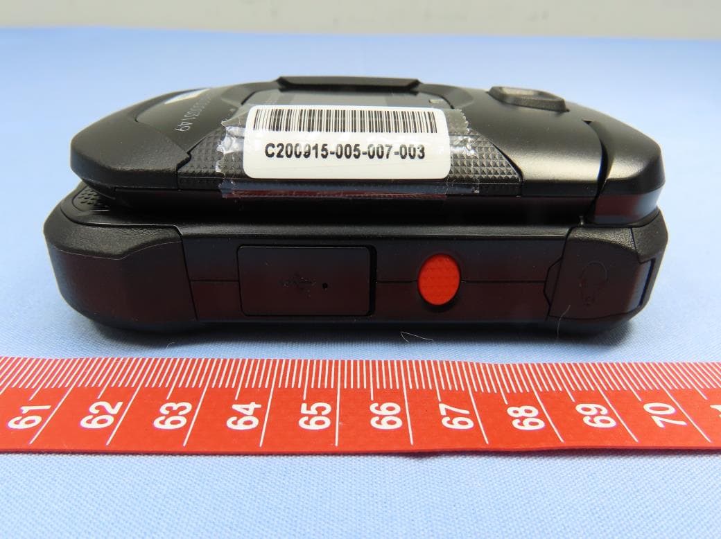
V65E4830
Feb 22, 2021Feature Phone
Equipment Class
PCE - PCS Licensed Transmitter held to ear
V65E7110
Dec 21, 2020Smart Phone
Equipment Class
5GM - Part 30 Mobile Transmitter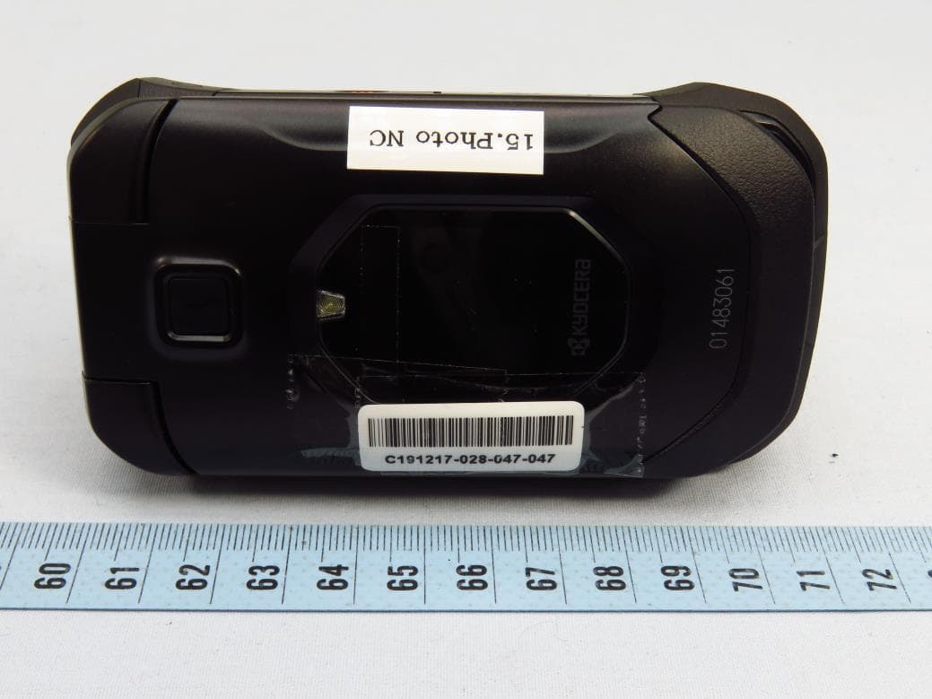
V65E4810
Mar 17, 2020Feature Phone
Equipment Class
PCE - PCS Licensed Transmitter held to ear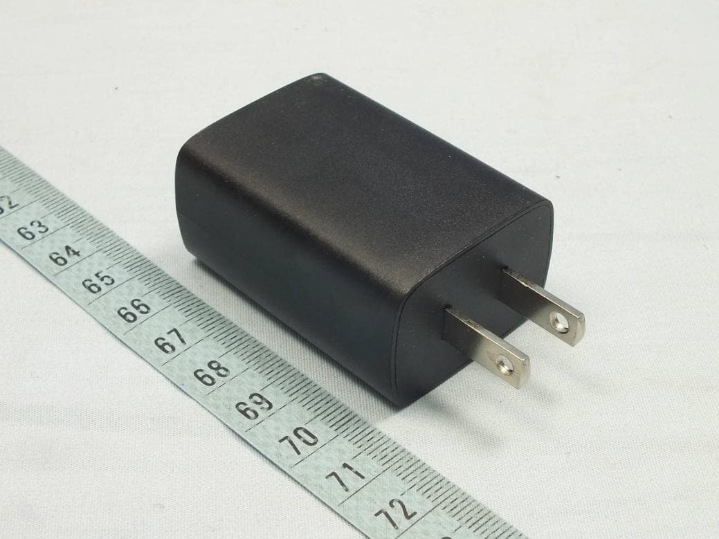
V65C6742
Nov 22, 2015UMTS/GSM Bar Phone
Equipment Class
DSS - Part 15 Spread Spectrum Transmitter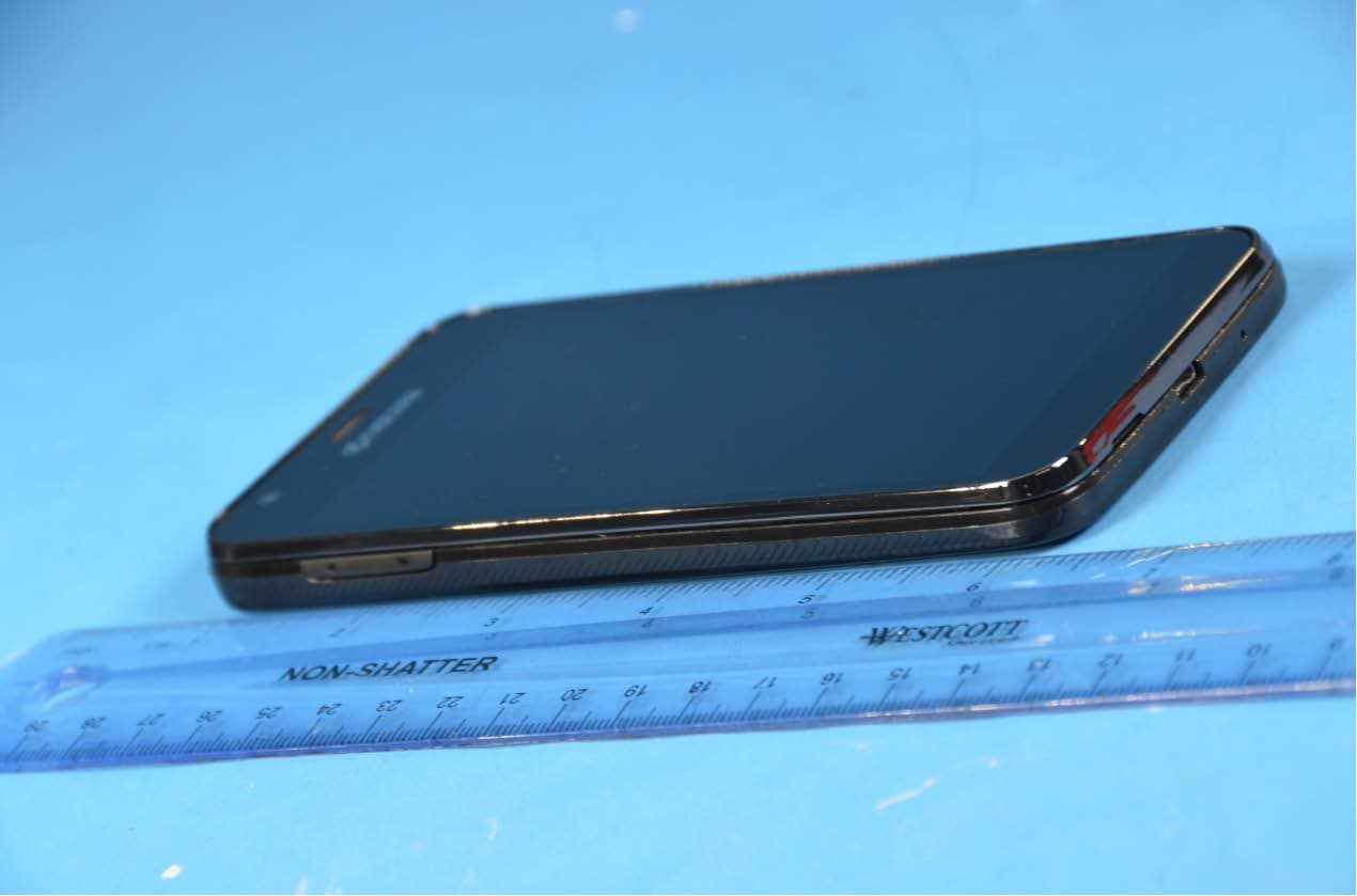
V65CD8100
Nov 05, 2015Multi-Band CDMA/LTE Phone with WLAN, Bluetooth and Nordic Transmitter
Equipment Class
DTS - Digital Transmission System