VLJ-BLINK1Wifi Baby Monitor
Binatone Electronics International Ltd.
Click to zoom
Application Details
- Equipment Class
- DTS - Digital Transmission System
- Date of Grant
- Feb 28, 2012
- Application Purpose
- Original Equipment
- Date of Application
- Feb 28, 2012
- Equipment Note
- Wifi Baby Monitor
- Frequency Range
- 2412.00000000 - 2462.00000000
- Country
- China
Documents & Files
Document Text
Text extracted from the exhibit documents filed with the FCC. Open a document above to read the original.
Users Manual
USERíS GUIDE BLINK1 / MBP2000BU / MSC3 BABY MONITOR USERíS GUIDE The features described in user's guide are subject to modifications without prior notice. This User's Guide provides you with all the information you need to get the most from your product. Before you can use the baby monitor, we recommend you insert and fully charge the battery in the parent unit, so that it continues to work if you disconnect it from the power supply to carry it to another location. Please read the Safety Instructions on page 6 before you install the units. Got everything? ï 1 x Baby Camera Unit ï 1 x Power adaptor for the Baby Camera Unit Welcome... to your new Motorola Baby Monitor! Thank you for purchasing the BLINK1/MBP2000BU/MSC3. Now you can see and hear your baby sleeping in another room or you can monitor your older children in their playroom. Please retain your original dated sales receipt for your records. For warranty service of your Motorola product, you will need to provide a copy of your dated sales receipt to confirm warranty status. Registration is not required for warranty coverage. For product related questions, please call: US and Canada 1-888-331-3383 UK0845 218 0890 On the Web: www.motorola.com 1.Photo Sensor (Night Vision Mode) 2.Camera Lens 3.Infared LEDs 4.Power LED 5.Microphone 6.Speaker 7.ON/OFF Switch 8.Power Adapter Connector 9.Antenna 10.Temperature Sensor 11.Pair Key Important guidelines for installing your Baby Monitor ï To use your Video Monitor Baby and Parent Unit together, you must be able to establish a radio link between them, and the range will be affected by environmental conditions. ï Any large metal object, like a refrigerator, a mirror, a filing cabinet, metallic doors or reinforced concrete between the Baby and Parent Unit may block the radio signal. ï The signal strength may also be reduced by other solid structures, like walls, or by radio or electrical equipment, such as TVs, computers, cordless or mobile phones, fluorescent lights or dimmer switches. ï Use of other 2.4GHz products, such as wireless networks (WiFi routers), Bluetooth Æ systems, or microwave ovens, may cause interference with this product, so keep the baby monitor away at least 5ft (1m) from these types of products, or turn them off if they appear to be causing interference. ï If the signal is weak, try moving the Parent and/or the Baby Unit to different positions in the rooms. Overview of Your Baby Unit 1 9 11 10 8 2 3 6 5 4 7 Table of contents5 ENGLISH Table of contents 1. Safety Instructions .....................................................................6 2. Getting Start ................................................................................8 3. Operation Mode ..........................................................................9 4. Direct Mode Monitoring ..........................................................12 5. Setup The Camera In Router Mode ........................................16 6. More Function Of Baby Monitor ..............................................28 7. Disposal Of The Device ............................................................36 8. Cleaning ....................................................................................37 9. General Information .................................................................39 6Safety Instructions 1. Safety Instructions WARNING This baby monitor is compliant with all relevant standards regarding electromagnetic fields and is, when handled as described in the User's Guide, safe to use. Therefore, always read the instructions in this User's Guide carefully before using the device. ï Adult assembly is required. Keep small parts away from children when assembling. ï This product is not a toy. Do not allow children to play with it. ï This baby monitor is not a substitute for responsible adult supervision. ï Keep this user's guide for future reference. ï Do not place the baby unit or cables in the cot / crib or within reach of the baby (the unit should be at least 3 feet away). ï Keep the cords out of reach of children. ï Do not cover the baby monitor with a towel or blanket. WARNING: STRANGULATION HAZARD - Keep the adapter cord out of baby's reach. NEVER place camera or cords within the cot / crib. Secure the cord some distance away from baby's reach. Never use extension cords with AC Adapters. Only use the AC Adapters provided. CAMERA SET UP & USE: ●Determine a location for the CAMERA that will provide the best view of your baby in his cot / crib. ●Place the CAMERA on a flat surface, such as a dresser, bureau, or shelf. ●NEVER place camera or cords within cot / crib. ●Secure the cord to the wall to keep cord away from the baby's reach. Safety Instructions7 ENGLISH ï Never use extension cords with power adapters. Only use the power adapters provided. ï Test this monitor and all its functions so that you are familiar with it prior to actual use. ï Do not use the baby monitor near water. ï Do not install the baby monitor near a heat source. ï Only use the chargers and power adapters provided. Do not use other chargers or power adapters as this may damage the device and battery pack. ï Do not touch the plug contacts with sharp or metal objects. 8Getting Started 2. Getting Started 2.1Baby Unit Power Supply 1.Connect the small plug of the power adapter to the baby unit and the other end to the electrical outlet. NOTE Only use the enclosed power adapter (5.9V DC / 1000mA). 2.Slide the ON/OFF switch to the ON position. The power LED will light up in green. 3.Slide the ON/OFF switch to the OFF position to turn the Baby Unit off. 9 ENLISH Operation Mode 3. Operation Mode There are three operation modes how the Baby Monitor connected to and viewed by the Parent Unit. 3.1 Local Monitoring in Direct Connect Mode: • Auto and Direct connection between Parent and Baby camera unit for in-house monitoring without the connection to WiFi Router. • Easy Setup. 10Operation Mode 3.2 Local Monitoring in Router Mode: • Parent and …
Text truncated - open the document above for the full version.
Users Manual
USERíS GUIDE BLINK1 / MBP2000BU / MSC3 BABY MONITOR USERíS GUIDE The features described in user's guide are subject to modifications without prior notice. This User's Guide provides you with all the information you need to get the most from your product. Before you can use the baby monitor, we recommend you insert and fully charge the battery in the parent unit, so that it continues to work if you disconnect it from the power supply to carry it to another location. Please read the Safety Instructions on page 6 before you install the units. Got everything? ï 1 x Baby Camera Unit ï 1 x Power adaptor for the Baby Camera Unit Welcome... to your new Motorola Baby Monitor! Thank you for purchasing the BLINK1/MBP2000BU/MSC3. Now you can see and hear your baby sleeping in another room or you can monitor your older children in their playroom. Please retain your original dated sales receipt for your records. For warranty service of your Motorola product, you will need to provide a copy of your dated sales receipt to confirm warranty status. Registration is not required for warranty coverage. For product related questions, please call: US and Canada 1-888-331-3383 UK0845 218 0890 On the Web: www.motorola.com 1.Photo Sensor (Night Vision Mode) 2.Camera Lens 3.Infared LEDs 4.Power LED 5.Microphone 6.Speaker 7.ON/OFF Switch 8.Power Adapter Connector 9.Antenna 10.Temperature Sensor 11.Pair Key Important guidelines for installing your Baby Monitor ï To use your Video Monitor Baby and Parent Unit together, you must be able to establish a radio link between them, and the range will be affected by environmental conditions. ï Any large metal object, like a refrigerator, a mirror, a filing cabinet, metallic doors or reinforced concrete between the Baby and Parent Unit may block the radio signal. ï The signal strength may also be reduced by other solid structures, like walls, or by radio or electrical equipment, such as TVs, computers, cordless or mobile phones, fluorescent lights or dimmer switches. ï Use of other 2.4GHz products, such as wireless networks (WiFi routers), Bluetooth Æ systems, or microwave ovens, may cause interference with this product, so keep the baby monitor away at least 5ft (1m) from these types of products, or turn them off if they appear to be causing interference. ï If the signal is weak, try moving the Parent and/or the Baby Unit to different positions in the rooms. Overview of Your Baby Unit 1 9 11 10 8 2 3 6 5 4 7 Table of contents5 ENGLISH Table of contents 1. Safety Instructions .....................................................................6 2. Getting Start ................................................................................8 3. Operation Mode ..........................................................................9 4. Direct Mode Monitoring ..........................................................12 5. Setup The Camera In Router Mode ........................................16 6. More Function Of Baby Monitor ..............................................28 7. Disposal Of The Device ............................................................36 8. Cleaning ....................................................................................37 9. General Information .................................................................39 6Safety Instructions 1. Safety Instructions WARNING This baby monitor is compliant with all relevant standards regarding electromagnetic fields and is, when handled as described in the User's Guide, safe to use. Therefore, always read the instructions in this User's Guide carefully before using the device. ï Adult assembly is required. Keep small parts away from children when assembling. ï This product is not a toy. Do not allow children to play with it. ï This baby monitor is not a substitute for responsible adult supervision. ï Keep this user's guide for future reference. ï Do not place the baby unit or cables in the cot / crib or within reach of the baby (the unit should be at least 3 feet away). ï Keep the cords out of reach of children. ï Do not cover the baby monitor with a towel or blanket. WARNING: STRANGULATION HAZARD - Keep the adapter cord out of baby's reach. NEVER place camera or cords within the cot / crib. Secure the cord some distance away from baby's reach. Never use extension cords with AC Adapters. Only use the AC Adapters provided. CAMERA SET UP & USE: ●Determine a location for the CAMERA that will provide the best view of your baby in his cot / crib. ●Place the CAMERA on a flat surface, such as a dresser, bureau, or shelf. ●NEVER place camera or cords within cot / crib. ●Secure the cord to the wall to keep cord away from the baby's reach. Safety Instructions7 ENGLISH ï Never use extension cords with power adapters. Only use the power adapters provided. ï Test this monitor and all its functions so that you are familiar with it prior to actual use. ï Do not use the baby monitor near water. ï Do not install the baby monitor near a heat source. ï Only use the chargers and power adapters provided. Do not use other chargers or power adapters as this may damage the device and battery pack. ï Do not touch the plug contacts with sharp or metal objects. 8Getting Started 2. Getting Started 2.1Baby Unit Power Supply 1.Connect the small plug of the power adapter to the baby unit and the other end to the electrical outlet. NOTE Only use the enclosed power adapter (5.9V DC / 1000mA). 2.Slide the ON/OFF switch to the ON position. The power LED will light up in green. 3.Slide the ON/OFF switch to the OFF position to turn the Baby Unit off. 9 ENLISH Operation Mode 3. Operation Mode There are three operation modes how the Baby Monitor connected to and viewed by the Parent Unit. 3.1 Local Monitoring in Direct Connect Mode: • Auto and Direct connection between Parent and Baby camera unit for in-house monitoring without the connection to WiFi Router. • Easy Setup. 10Operation Mode 3.2 Local Monitoring in Router Mode: • Parent and …
Text truncated - open the document above for the full version.
Block Diagram
WiFi module WiFi module MCU Wifi module SPI Flash 4MB USB BUS 3.3V SPI BUS 3.3V Antenna (0dBi monopol ) 3.3V Nuvoton W55VA93 4MB Analog Microphone DB0-15 DAC output 3.3V e ) Cmos Sensor 7675 MclkPclk A udio amp IC - ISD8101SYI 30mm Speaker 3.3V DAC output IR X 8 GPIO 3.3V LED X 1 GPIO Light sensor 3.3V 3.3V GPIO GPIO Speaker Crystal 27MHz Reset 3.3V Pairing Switch DC jack 5V 1000mA DC/DC AP3406 3.3V On/Off SW 5V 2V DC/DC AP3406
Block Diagram
WiFi module WiFi module MCU Wifi module SPI Flash 4MB USB BUS 3.3V SPI BUS 3.3V Antenna (0dBi monopol ) 3.3V Nuvoton W55VA93 4MB Analog Microphone DB0-15 DAC output 3.3V e ) Cmos Sensor 7675 MclkPclk A udio amp IC - ISD8101SYI 30mm Speaker 3.3V DAC output IR X 8 GPIO 3.3V LED X 1 GPIO Light sensor 3.3V 3.3V GPIO GPIO Speaker Crystal 27MHz Reset 3.3V Pairing Switch DC jack 5V 1000mA DC/DC AP3406 3.3V On/Off SW 5V 2V DC/DC AP3406
External Photos
EXHIBIT B - EUT EXTERNAL PHOTOGRAPHS EUT – Front View EUT – Rear View EUT – Adapter View EUT – Adapter Label View
External Photos
EXHIBIT B - EUT EXTERNAL PHOTOGRAPHS EUT – Front View EUT – Rear View EUT – Adapter View EUT – Adapter Label View
ID Label/Location Info
EXHIBIT A - FCC ID LABELING AND LOCATION FCC ID Label FCC ID Label Location Label here The label shown shall be permanently affixed at a conspicuous location on the device and be readily visible to the user at the time purchase (Labeling requirements per 2.925)
ID Label/Location Info
EXHIBIT A - FCC ID LABELING AND LOCATION FCC ID Label FCC ID Label Location Label here The label shown shall be permanently affixed at a conspicuous location on the device and be readily visible to the user at the time purchase (Labeling requirements per 2.925)
Internal Photos
EXHIBIT C - EUT INTERNAL PHOTOGRAPHS EUT – Cover off View 1 EUT – Cover off View 2 EUT – Main Board Top View 1 EUT – Main Board Top View 2 Antenna Location EUT – Main Board Bottom View EUT – RF Module Board Top View EUT – RF Module Board Bottom View EUT – Motor View EUT – Camera Board Top View EUT – Camera Board Bottom View
Internal Photos
EXHIBIT C - EUT INTERNAL PHOTOGRAPHS EUT – Cover off View 1 EUT – Cover off View 2 EUT – Main Board Top View 1 EUT – Main Board Top View 2 Antenna Location EUT – Main Board Bottom View EUT – RF Module Board Top View EUT – RF Module Board Bottom View EUT – Motor View EUT – Camera Board Top View EUT – Camera Board Bottom View
Operational Description
1. Circuit Description This device mainly consist with two parts which are RF and baseband. The RF part is using for wifi 802.11 b/g/n system. The antenna using for the RF is a monopole 0dBi antenna. The baseband including a MCU which control the motor movement, Cmos sensor for video, IR led, heat sensor and the power management. There are total two type of the ground which is analogue ground and the digital the ground. The analogue ground is only for the Mic. All other components are using the digital grounding. There are two type of the voltage supply to the MCU, which the 5V is supplied from the adaptor to the device and the 5V will be regulated by the LDO and given two voltage which are 3.3V and 2V. These two voltages will supply to the MCU.
Operational Description
1. Circuit Description This device mainly consist with two parts which are RF and baseband. The RF part is using for wifi 802.11 b/g/n system. The antenna using for the RF is a monopole 0dBi antenna. The baseband including a MCU which control the motor movement, Cmos sensor for video, IR led, heat sensor and the power management. There are total two type of the ground which is analogue ground and the digital the ground. The analogue ground is only for the Mic. All other components are using the digital grounding. There are two type of the voltage supply to the MCU, which the 5V is supplied from the adaptor to the device and the 5V will be regulated by the LDO and given two voltage which are 3.3V and 2V. These two voltages will supply to the MCU.
Schematics
B 1 2 REV: SIZE: CODE: DRAWN: DATED: DATED: CHECKED:QUALITY CONTROL: DATED: DATED: RELEASED: COMPANY:TITLE: DRAWING NO: SHEET: OF SCALE: REVISION RECORD APPROVED: ECO NO: ABD DATE: 1 2 3 4 5 6 DCAB C LTR LIGHT_DET Connect to CMOS sensor Connect to CMOS sensor Boundary sensor SW IR1IR2 IR3IR4 IR5IR6 IR7IR8 R6 R7 R8 R9 R97 12 PT2 LED2 Q4 R32 R33 R36 12 J6 123456789 10 11 121314151617181920 CON1 1 2 3 SW1 R1 R2 Q5 R39 R40 R3R4 R5 R10R11R12 R13R14R15R16 VD33 [1] AIN3 #LED1 VD33 VS [1,2] VD33 [1,2] VS VS [2] GPC8 [2] GPC9 [2] GPC10 [2] GPC11 [2] GPC12 [2] GPC13 [2] GPC14 [2] GPB1 [1] IR_CONTROL [1] #LED1 [2] CMOS_RESET [1] AIN3 [2] GPC15 [2] GPB13 [2] GPB3 [2] GPB2 [2] GPB14 [1] GPC6 [2] GPB0 VD33 [1] GPC6 VD33 [1] IR_CONTROL VS VS VS 1,2,4,6,7 1,2,3,4,6,7 11 1 VS R87 1 NC 2 AGND 3 SDATA 4 VAA 5 SCK 6 RESET 7 FVALID 8 STANDBY 9 LVALID 10 VDD 11 VDDIO 12 D7 13 MCLK 14 D6 15 DGND 16 D5 17 PCLK 18 D4 19 D0 20 D3 21 D1 22 D2 23 NC3 24 NC2 J3 R81 C74 R78 C75 R76 R82 R85 C73 R83 R77 C76 C77 R86 R49 R51 C90 C91 C92 G I O 1 2 3 U5 C34 C1 C2 [1] VD33 [1,2] VS [1] GPB1 [1] GPB0 [1] CMOS_RESET VS VS VS VS VS VS VS VS GPB[13:14] GPC[8:15] GPB14 GPB0 S_PCLK GPB1 GPC15 S_VD30 S_VSYNC S_CLK GPC8 GPB13 GPB13 GPC9 GPB2GPB3 S_VD30 S_AVD30 S_HSYNC GPC10GPC14GPC13 GPB14 GPC12GPC11 S_AVD30 VS VS S_VD30 VS VS VS VS Title SizeDocument NumberRev Date:Sheetof18 A3 Sunday, April 24, 2011 ? A B C D 54321 D C B A 12345 2,4,5,6,7 2,5 2,3,4,5,6,7 2 2 5 5 2 2 2 7 7 7 7 7 7 7 4 2 5 spk_en swap with wifi_en RS-Pin11 RS-Pin12 general purpose peak EMI reduction IC C27 C22 C4 R3 C14 C5 C15 C20 L4 C6 C33 L7 R12 R4 C18 R6 C3 R13 C23 C26 R7 C25 L6 1 SPCLK/GPB1/UHL_DM1/SD1D0 2 SCLKO/GPB0/UHL_DP1/SD1D1 3 ISDA/GPB14/LMVSYNC 4 ISCK/GPB13/WDT_NRST 5 SPI0_CLK/GPD12 6 SPI0_NCS0/GPD13 7 SPI0_DI/GPD14 8 SPI0_DO/GPD15 9 SDD2/GPE4 10 SDD3/GPE5 11 SDCMD/GPE6 12 SDCLK/GPE7 13 SDD0/GPE2 14 SDD1/GPE3 15 XIN 16 XOUT 22 MVDD 19 MVDDQ 18 MVSSQ 20 MVSSQ 21 MVDDQ 17 VDD18 23 MVREF 24 USB/PLL_VDD18 25 USB_VSS 26 USB_DM 27 USB_DP 28 USB_VDD33 29 USB_REXT 30 MVDD 31 VSS33 32 LVD17/GPE1/SVSYNC 33 LVD16/GPE0/SHSYNC 34 LVD15/GPC15/SPD7 35 LVD14/GPC14/SPD6 36 LVD13/GPC13/SPD5 37 LVD12/GPC12/SPD4 38 LVD11/GPC11/SPD3 39 LVD10/GPC10/SPD2 40 LVD9/GPC9/SPD1 41 LVD8/GPC8/SPD0 42 LVD7/GPC7 43 LVD6/GPC6 44 LVD5/GPC5 45 LVD4/GPC4 46 LVD3/GPC3 47 LVD2/GPC2 48 LVD1/GPC1 49 LVD0/GPC0 50 LVDE/GPD11/WDT_NRST 51 LVSYNC/GPD10 52 LHSYNC/GPD9 53 VDD18 54 LPCLK/GPB15 55 VDD33 56 ADC_VSS33 57 TP_YM 58 TP_XM 59 TP_XP 60 TP_YP 61 ADC_VDD33 62 ADC_AIN0/MICP 63 ADC_AIN1/MICM 64 ADC_AIN2 97 ADAC_HPR 98 ADAC_VSS33 99 ADAC_VREF 100 ADAC_VDD33 101 ADAC_VDD33 102 VDD18 103 GPA7 104 ND0 105 ND1 106 ND2 107 ND3 108 ND4 109 ND5 110 ND6 111 ND7 112 NNBUSY1/GPD6/SD2D2 113 NNBUSY0/GPD5/SD2D3 114 NNWR/GPD8/SD2CMD 115 NNRE/GPD7/SD2CLK 116 NCLE/GPE11 117 NALE/GPE10 118 NNCS1/GPE9/SD2D0 119 VSS33 120 NNCS0/GPE8/SD2D1 121 VDD33 122 URTX/GPA10/SPI1_NCS1 123 URRX/GPA11/LMVSYNC 124 SPD1/GPB6/I2SDIN 125 SPD0/GPB5/I2SDOUT/SD1D2 126 SFIELD/GPB4/I2S_WS/SD1D3 127 SVSYNC/GPB3/I2S_BCLK/SD1CMD 128 SHSYNC/GPB2/I2S_MCLK/SD1CLK 65 MVSS 66 ADC_AIN3 67 RTC_XOUT 68 RTC_XIN 69 RTC_NWAKEUP 70 RTC_PWREN 71 RTC_VDD 72 VDD33 73 GPA6/SPI1_NCS1 74 GPA5/SPI0_NCS1 75 GPA4/UHL_DM1 76 GPA3/UHL_DP1 77 GPA2/LMVSYNC 78 GPA1/SD_NCD 79 GPA0 80 NRST 81 TCK/GPD0/SPI1_NCS1/PWM0 82 TMS/GPD1/HUR_TX/PWM1 83 TDI/GPD2/HUR_RX/PWM2 84 TDO/GPD3/HUR_CTS/PWM3 85 NTRST/GPD4/HUR_RTS/SPI0_NCS1 86 USB_DET 87 VDD18 88 MVSS 89 MVREF 90 MVSSQ 91 MVDDQ 92 MVDDQ 93 ADAC_HPVSS33 94 ADAC_HPVDD33 95 ADAC_HPL 96 MVSSQ U1 R11 C1 C8 R8 C2 C7 R5 C24 C35 C36 L2 L1 C16 C9 C19C21 R9 C28 C13 C12 C87 C88 C89 1 /CS 2 DO 3 /WP 4 GND 5 DI 6 CLK 7 /HOLD 8 VCC U9 R55R57 C93 C94 X1 R10 C30 1 1 PAD3 1 1 PAD4 1 1 PAD5 1 1 PAD6 1 1 PAD7 1 1 PAD8 1 1 PAD9 1 1 PAD20 C34 C17 1 1 PAD13 1 1 PAD14 1 1 PAD15 1 1 PAD16 1 1 PAD17 1 1 PAD12 1 1 PAD18 1 XIN/CLKIN 2 XOUT 3 FS 4 GND 5 MODOUT 6 MR 7 SSEXTR 8 VDD U14 R15 R16 R17 R20 R21 L5 C73 R26 R30 R31 R32 R33 1 1 PAD19 1 1 PAD21 1 1 PAD22 1 1 PAD23 1 1 PAD24 [1,2,3,5,6,7,8] VD33 [1,2] VD18 [1,2,3,4,5,6,7,8] VS [2] USBDP [2] USBDM [8] GPB0 [8] GPB1 [3] MOTOR_A+ [3] MOTOR_A- [3] MOTOR_B+ [3] MOTOR_B- [6] USB_HS_D+ [6] USB_HS_D- [5] SPK_EN [8] CMOS_RESET VD33 VDD33 VD18 VD18 VS VS VS VD33 VS VD33 VD33 VD33 VS VS VS VS VS VS VS VS VS VSVS VS VS AIN[2:3] GPB[13:14] [5] MIC[0:1] [4] ND[0:7] GPC[8:15] MVDDQ GPB0 AIN2 VD18 AIN3 LVD4 GPC8 LVD5 MIC0 USB_DET NTRST NTRST GPC9 MOTOR_A-MOTOR_A- RTC_WKUP GPD13 VDD33 GPC10 GPB13 GPC11 MOTOR_A+ MIC1 ADAVREF GPD12 USBVDD33 NRESET NRESET USBREXT DAC1 MOTOR_B- MOTOR_B- ND6 ND7 PLLVDD18 GPB14 MOTOR_B+ GPC15 X12 DAC0 USBDM GPD15 GPB1 RTC_PWR_ENUSBDP ND2ND0 GPC12 GPC13 GPD14 X11 GPC14 MVDDQ MVDDQ MVDDQ MVDDQ MVDDQ MVDDQ MVDDQ MVREF MVREF VD18 VS VS VD33 VD33 VD33 VDD33 VDD33 VDD33 ADCVSS ADAVDD33ADAVDD33ADAVREF USBVDD33 VS VS DAC1 VD18 VD18 VD18 VD18 ADAVDD33 PLLVDD18 ADCVDD DAC0 VS VS MVREF USB_HS_D+ USB_HS_D- GPD12 GPD15 GPD14 VD33 VS VD33 GPD13 VS VS VS AIN3 GPA11GPA10 VS [1,2,3,5,6,7,8] VD33 NRESET VS ADAVDD33 VD18RTC_VDD VS RTC_VDD #LED1 VS [3] UPMOTOR+ [3] UPMOTOR- [3] DOWNMOTOR+ [3] DOWNMOTOR- [7] GPA5 [3] GPD6 [8] IR_CONTROL [8] GPC6 [8] GPB3 [8] GPB2 [6] #WIFI_PW_EN [1] MODOUT VD33 VD33 VD33 X12 X11 [1] MODOUT VS VS VS VS VS ? Sunday, April 24, 2011 A3 82ofSheetDate: RevDocument NumberSize Title Vout =3.3V A B C D 54321 D C B A 12345 1,7 1,5 1,4,5,6,7 VD18-> 2V switch DC Jack power supply B 2,3,4,5,6,7 4 VIN 1 RUN 3 SW 5 FB 2 GND U2 4 VIN 1 RUN 3 SW 5 FB 2 GND U3 C49 C40 R27 R38 C50 C41 R35 L9 L11 R28 R40 C43 L15 L10 C45 C53 C48 L14 C39 C46 R34 C47 L13 C58 C44 R23 R22 D5 R41 R42 VAR5 FUSE2 L3 L20 JACK2 1 3 2 SW1 Q206 R1 ZG202 1 2 3 4 CON1 1 1 PAD1 1 1 PAD2 1 1 PAD10 1 1 PAD11 [1,2]VD18 [1,2,3,5,6,7,8] VD33 VIN VD33 VD18 VS VS VS VS VSVS VS VS VS VS VS VS VS VSVS [2,3] VIN VS VSVS [1,2,3,4,5,6,7,8]VS VS [1]USBDP [1]USBDM VS [1,4] ND0 ? Sunday, April 24, 2011 A3 83ofSheetDate: RevSize Title A B C D 54321 D C B A 12345 1 1 VBoff =0.6V Vin =3.6V => Vb = 0.59v Vin =3.7V => Vb = 0.606v Vin =3.8V => Vb…
Text truncated - open the document above for the full version.
Schematics
B 1 2 REV: SIZE: CODE: DRAWN: DATED: DATED: CHECKED:QUALITY CONTROL: DATED: DATED: RELEASED: COMPANY:TITLE: DRAWING NO: SHEET: OF SCALE: REVISION RECORD APPROVED: ECO NO: ABD DATE: 1 2 3 4 5 6 DCAB C LTR LIGHT_DET Connect to CMOS sensor Connect to CMOS sensor Boundary sensor SW IR1IR2 IR3IR4 IR5IR6 IR7IR8 R6 R7 R8 R9 R97 12 PT2 LED2 Q4 R32 R33 R36 12 J6 123456789 10 11 121314151617181920 CON1 1 2 3 SW1 R1 R2 Q5 R39 R40 R3R4 R5 R10R11R12 R13R14R15R16 VD33 [1] AIN3 #LED1 VD33 VS [1,2] VD33 [1,2] VS VS [2] GPC8 [2] GPC9 [2] GPC10 [2] GPC11 [2] GPC12 [2] GPC13 [2] GPC14 [2] GPB1 [1] IR_CONTROL [1] #LED1 [2] CMOS_RESET [1] AIN3 [2] GPC15 [2] GPB13 [2] GPB3 [2] GPB2 [2] GPB14 [1] GPC6 [2] GPB0 VD33 [1] GPC6 VD33 [1] IR_CONTROL VS VS VS 1,2,4,6,7 1,2,3,4,6,7 11 1 VS R87 1 NC 2 AGND 3 SDATA 4 VAA 5 SCK 6 RESET 7 FVALID 8 STANDBY 9 LVALID 10 VDD 11 VDDIO 12 D7 13 MCLK 14 D6 15 DGND 16 D5 17 PCLK 18 D4 19 D0 20 D3 21 D1 22 D2 23 NC3 24 NC2 J3 R81 C74 R78 C75 R76 R82 R85 C73 R83 R77 C76 C77 R86 R49 R51 C90 C91 C92 G I O 1 2 3 U5 C34 C1 C2 [1] VD33 [1,2] VS [1] GPB1 [1] GPB0 [1] CMOS_RESET VS VS VS VS VS VS VS VS GPB[13:14] GPC[8:15] GPB14 GPB0 S_PCLK GPB1 GPC15 S_VD30 S_VSYNC S_CLK GPC8 GPB13 GPB13 GPC9 GPB2GPB3 S_VD30 S_AVD30 S_HSYNC GPC10GPC14GPC13 GPB14 GPC12GPC11 S_AVD30 VS VS S_VD30 VS VS VS VS Title SizeDocument NumberRev Date:Sheetof18 A3 Sunday, April 24, 2011 ? A B C D 54321 D C B A 12345 2,4,5,6,7 2,5 2,3,4,5,6,7 2 2 5 5 2 2 2 7 7 7 7 7 7 7 4 2 5 spk_en swap with wifi_en RS-Pin11 RS-Pin12 general purpose peak EMI reduction IC C27 C22 C4 R3 C14 C5 C15 C20 L4 C6 C33 L7 R12 R4 C18 R6 C3 R13 C23 C26 R7 C25 L6 1 SPCLK/GPB1/UHL_DM1/SD1D0 2 SCLKO/GPB0/UHL_DP1/SD1D1 3 ISDA/GPB14/LMVSYNC 4 ISCK/GPB13/WDT_NRST 5 SPI0_CLK/GPD12 6 SPI0_NCS0/GPD13 7 SPI0_DI/GPD14 8 SPI0_DO/GPD15 9 SDD2/GPE4 10 SDD3/GPE5 11 SDCMD/GPE6 12 SDCLK/GPE7 13 SDD0/GPE2 14 SDD1/GPE3 15 XIN 16 XOUT 22 MVDD 19 MVDDQ 18 MVSSQ 20 MVSSQ 21 MVDDQ 17 VDD18 23 MVREF 24 USB/PLL_VDD18 25 USB_VSS 26 USB_DM 27 USB_DP 28 USB_VDD33 29 USB_REXT 30 MVDD 31 VSS33 32 LVD17/GPE1/SVSYNC 33 LVD16/GPE0/SHSYNC 34 LVD15/GPC15/SPD7 35 LVD14/GPC14/SPD6 36 LVD13/GPC13/SPD5 37 LVD12/GPC12/SPD4 38 LVD11/GPC11/SPD3 39 LVD10/GPC10/SPD2 40 LVD9/GPC9/SPD1 41 LVD8/GPC8/SPD0 42 LVD7/GPC7 43 LVD6/GPC6 44 LVD5/GPC5 45 LVD4/GPC4 46 LVD3/GPC3 47 LVD2/GPC2 48 LVD1/GPC1 49 LVD0/GPC0 50 LVDE/GPD11/WDT_NRST 51 LVSYNC/GPD10 52 LHSYNC/GPD9 53 VDD18 54 LPCLK/GPB15 55 VDD33 56 ADC_VSS33 57 TP_YM 58 TP_XM 59 TP_XP 60 TP_YP 61 ADC_VDD33 62 ADC_AIN0/MICP 63 ADC_AIN1/MICM 64 ADC_AIN2 97 ADAC_HPR 98 ADAC_VSS33 99 ADAC_VREF 100 ADAC_VDD33 101 ADAC_VDD33 102 VDD18 103 GPA7 104 ND0 105 ND1 106 ND2 107 ND3 108 ND4 109 ND5 110 ND6 111 ND7 112 NNBUSY1/GPD6/SD2D2 113 NNBUSY0/GPD5/SD2D3 114 NNWR/GPD8/SD2CMD 115 NNRE/GPD7/SD2CLK 116 NCLE/GPE11 117 NALE/GPE10 118 NNCS1/GPE9/SD2D0 119 VSS33 120 NNCS0/GPE8/SD2D1 121 VDD33 122 URTX/GPA10/SPI1_NCS1 123 URRX/GPA11/LMVSYNC 124 SPD1/GPB6/I2SDIN 125 SPD0/GPB5/I2SDOUT/SD1D2 126 SFIELD/GPB4/I2S_WS/SD1D3 127 SVSYNC/GPB3/I2S_BCLK/SD1CMD 128 SHSYNC/GPB2/I2S_MCLK/SD1CLK 65 MVSS 66 ADC_AIN3 67 RTC_XOUT 68 RTC_XIN 69 RTC_NWAKEUP 70 RTC_PWREN 71 RTC_VDD 72 VDD33 73 GPA6/SPI1_NCS1 74 GPA5/SPI0_NCS1 75 GPA4/UHL_DM1 76 GPA3/UHL_DP1 77 GPA2/LMVSYNC 78 GPA1/SD_NCD 79 GPA0 80 NRST 81 TCK/GPD0/SPI1_NCS1/PWM0 82 TMS/GPD1/HUR_TX/PWM1 83 TDI/GPD2/HUR_RX/PWM2 84 TDO/GPD3/HUR_CTS/PWM3 85 NTRST/GPD4/HUR_RTS/SPI0_NCS1 86 USB_DET 87 VDD18 88 MVSS 89 MVREF 90 MVSSQ 91 MVDDQ 92 MVDDQ 93 ADAC_HPVSS33 94 ADAC_HPVDD33 95 ADAC_HPL 96 MVSSQ U1 R11 C1 C8 R8 C2 C7 R5 C24 C35 C36 L2 L1 C16 C9 C19C21 R9 C28 C13 C12 C87 C88 C89 1 /CS 2 DO 3 /WP 4 GND 5 DI 6 CLK 7 /HOLD 8 VCC U9 R55R57 C93 C94 X1 R10 C30 1 1 PAD3 1 1 PAD4 1 1 PAD5 1 1 PAD6 1 1 PAD7 1 1 PAD8 1 1 PAD9 1 1 PAD20 C34 C17 1 1 PAD13 1 1 PAD14 1 1 PAD15 1 1 PAD16 1 1 PAD17 1 1 PAD12 1 1 PAD18 1 XIN/CLKIN 2 XOUT 3 FS 4 GND 5 MODOUT 6 MR 7 SSEXTR 8 VDD U14 R15 R16 R17 R20 R21 L5 C73 R26 R30 R31 R32 R33 1 1 PAD19 1 1 PAD21 1 1 PAD22 1 1 PAD23 1 1 PAD24 [1,2,3,5,6,7,8] VD33 [1,2] VD18 [1,2,3,4,5,6,7,8] VS [2] USBDP [2] USBDM [8] GPB0 [8] GPB1 [3] MOTOR_A+ [3] MOTOR_A- [3] MOTOR_B+ [3] MOTOR_B- [6] USB_HS_D+ [6] USB_HS_D- [5] SPK_EN [8] CMOS_RESET VD33 VDD33 VD18 VD18 VS VS VS VD33 VS VD33 VD33 VD33 VS VS VS VS VS VS VS VS VS VSVS VS VS AIN[2:3] GPB[13:14] [5] MIC[0:1] [4] ND[0:7] GPC[8:15] MVDDQ GPB0 AIN2 VD18 AIN3 LVD4 GPC8 LVD5 MIC0 USB_DET NTRST NTRST GPC9 MOTOR_A-MOTOR_A- RTC_WKUP GPD13 VDD33 GPC10 GPB13 GPC11 MOTOR_A+ MIC1 ADAVREF GPD12 USBVDD33 NRESET NRESET USBREXT DAC1 MOTOR_B- MOTOR_B- ND6 ND7 PLLVDD18 GPB14 MOTOR_B+ GPC15 X12 DAC0 USBDM GPD15 GPB1 RTC_PWR_ENUSBDP ND2ND0 GPC12 GPC13 GPD14 X11 GPC14 MVDDQ MVDDQ MVDDQ MVDDQ MVDDQ MVDDQ MVDDQ MVREF MVREF VD18 VS VS VD33 VD33 VD33 VDD33 VDD33 VDD33 ADCVSS ADAVDD33ADAVDD33ADAVREF USBVDD33 VS VS DAC1 VD18 VD18 VD18 VD18 ADAVDD33 PLLVDD18 ADCVDD DAC0 VS VS MVREF USB_HS_D+ USB_HS_D- GPD12 GPD15 GPD14 VD33 VS VD33 GPD13 VS VS VS AIN3 GPA11GPA10 VS [1,2,3,5,6,7,8] VD33 NRESET VS ADAVDD33 VD18RTC_VDD VS RTC_VDD #LED1 VS [3] UPMOTOR+ [3] UPMOTOR- [3] DOWNMOTOR+ [3] DOWNMOTOR- [7] GPA5 [3] GPD6 [8] IR_CONTROL [8] GPC6 [8] GPB3 [8] GPB2 [6] #WIFI_PW_EN [1] MODOUT VD33 VD33 VD33 X12 X11 [1] MODOUT VS VS VS VS VS ? Sunday, April 24, 2011 A3 82ofSheetDate: RevDocument NumberSize Title Vout =3.3V A B C D 54321 D C B A 12345 1,7 1,5 1,4,5,6,7 VD18-> 2V switch DC Jack power supply B 2,3,4,5,6,7 4 VIN 1 RUN 3 SW 5 FB 2 GND U2 4 VIN 1 RUN 3 SW 5 FB 2 GND U3 C49 C40 R27 R38 C50 C41 R35 L9 L11 R28 R40 C43 L15 L10 C45 C53 C48 L14 C39 C46 R34 C47 L13 C58 C44 R23 R22 D5 R41 R42 VAR5 FUSE2 L3 L20 JACK2 1 3 2 SW1 Q206 R1 ZG202 1 2 3 4 CON1 1 1 PAD1 1 1 PAD2 1 1 PAD10 1 1 PAD11 [1,2]VD18 [1,2,3,5,6,7,8] VD33 VIN VD33 VD18 VS VS VS VS VSVS VS VS VS VS VS VS VS VSVS [2,3] VIN VS VSVS [1,2,3,4,5,6,7,8]VS VS [1]USBDP [1]USBDM VS [1,4] ND0 ? Sunday, April 24, 2011 A3 83ofSheetDate: RevSize Title A B C D 54321 D C B A 12345 1 1 VBoff =0.6V Vin =3.6V => Vb = 0.59v Vin =3.7V => Vb = 0.606v Vin =3.8V => Vb…
Text truncated - open the document above for the full version.
Test Report
Note: This test report is prepared for the customer shown above and for the equipment described herein. It may not be duplicated or used in part without prior written consent from Bay Area Compliance Laboratories Corp. This report must not be used by the customer to claim product certification, approval, or endorsement by NVLAP*, or any agency of the Federal Government. * This report contains data that are not covered by the NVLAP accreditation and are marked with an asterisk “★” (Rev.2) FCC PART 15.247 TEST REPORT For Binatone Electronics International Limited Floor 23A, 9 Des Voeux Road West, Sheung Wan, Hong Kong Report Type: Original Report Product Type: Wifi Baby monitor Test Engineer: Brown Lu Report Number: R1DG111130003-00 Report Date: 2012-02-28 Reviewed By: Alvin Huang EMC Engineer Test Laboratory: Bay Area Compliance Laboratories Corp. (Shenzhen) 6/F, the 3rd Phase of WanLi Industrial Building, ShiHua Road, FuTian Free Trade Zone Shenzhen, Guangdong, China Tel: +86-755-33320018 Fax: +86-755-33320008 www.baclcorp.com.cn FCC ID: VLJ-BLINK1 Bay Area Compliance Laboratories Corp. (Shenzhen) Report No.: R1DG111130003-00 FCC Part15.247 Page 2 of 58 TABLE OF CONTENTS GENERAL INFORMATION.......................................................................................................................................4 PRODUCT DESCRIPTION FOR EQUIPMENT UNDER TEST (EUT) .....................................................................................4 OBJECTIVE...................................................................................................................................................................4 RELATED SUBMITTAL(S)/GRANT(S).............................................................................................................................4 TEST METHODOLOGY..................................................................................................................................................4 TEST FACILITY.............................................................................................................................................................5 SYSTEM TEST CONFIGURATION ......................................................…
Text truncated - open the document above for the full version.
Contact Information
Applicant
Sam Lee(Product Director)
Test Firm
Bay Area Compliance Laboratory Corp. (Shenzhen)John Chan
Technical Specifications
| # | Rule Parts | Frequency Range | Power Output |
|---|---|---|---|
| 3 | 15C | 2.41 GHz - 2.46 GHz | 28.00 mW |
Other Applications from Binatone Electronics International Ltd.

VLJ-NV531BU
Jul 03, 2022Video Baby Monitor
Equipment Class
DSS - Part 15 Spread Spectrum Transmitter
VLJ-MH002W
Mar 02, 2021Bluetooth Headset
Equipment Class
DSS - Part 15 Spread Spectrum Transmitter
VLJ-ST600
Feb 09, 20215-in-1 Nursery Humidifier
Equipment Class
DSS - Part 15 Spread Spectrum Transmitter
VLJ-SP025
Feb 01, 2021Portable Bluetooth Music Speaker
Equipment Class
DCD - Part 15 Low Power Transmitter Below 1705 kHz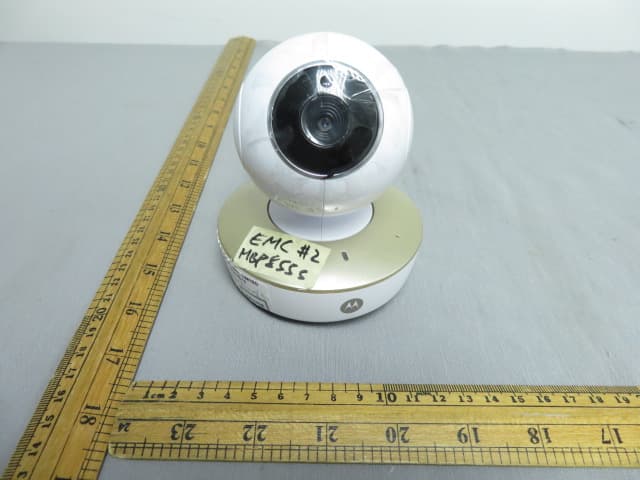
VLJ-MBP855BU
Dec 17, 20205inch Wi-Fi Video Baby Monitor
Equipment Class
DSS - Part 15 Spread Spectrum Transmitter