VW4A09-0490ATAVRRZ600
Microchip Technology Inc.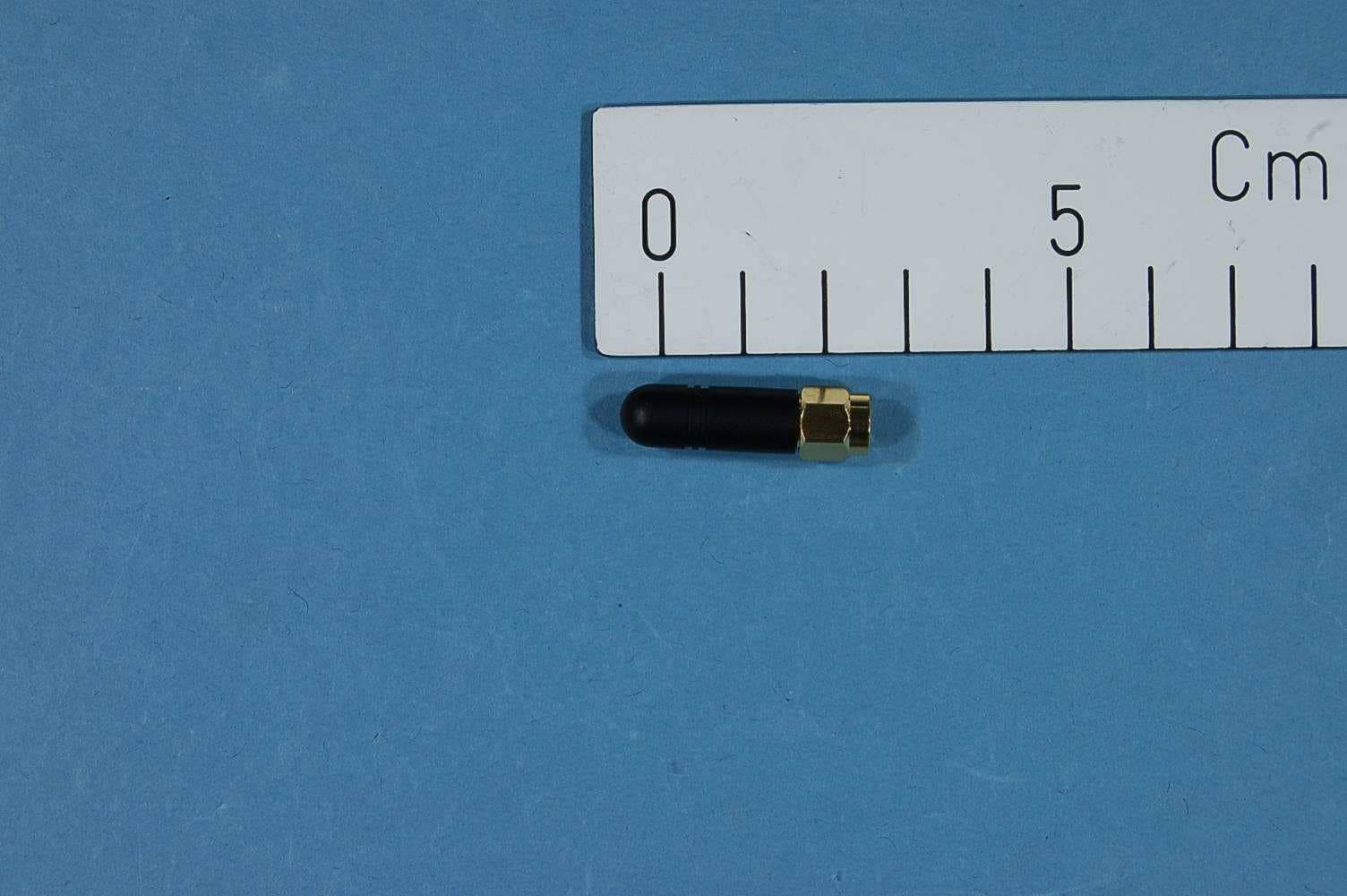
Click to zoom
Application Details
- Equipment Class
- DTS - Digital Transmission System
- Date of Grant
- Mar 17, 2010
- Application Purpose
- Original Equipment
- Date of Application
- Mar 17, 2010
- Equipment Note
- ATAVRRZ600
- Frequency Range
- 2405.00000000 - 2480.00000000
- Company
- Microchip Technology Inc.
- Country
- United States
Documents & Files
Document Text
Text extracted from the exhibit documents filed with the FCC. Open a document above to read the original.
Users Manual
AVR600: RZ600 HW Manual Features • Contains the full selection of AT86RF family radio transceivers. • Covers the 2.4GHz ISM band and 700, 800 and 900 MHz frequency bands. • In total 3 pair of radio transceivers are available – one pair per radio transceiver. • Two AT32UC3A3256 based USB host boards are included - Based on Atmel ® AVR ® UC3 core - 80 Dhrystone MIPS and Draws Only 40 mA at 66 MHz - Low, full and high speed USB compliant - Ideal for PC to RF gateways, packet sniffers and network commissioning tools • On board ID chip for easy IEEE MAC address • Stub antennas for all frequency bands 1 Introduction The RZ600 kit is an evaluation kit for the Atmel AT86RF family of radio frequency devices. The family contains the two 2.4 GHz device AT86RF230 and AT86RF231. These are highly acclaimed networking devices within low power personal area networks. In addition to this the world’s first IEEE 802.15.4 enabled sub gigahertz radio is provided – the AT86RF212. With the kit you also receive two AVR UC3 based host nodes that can be used to evaluate a point to point network connection. That being said; the RZ600 radio boards sport an Atmel standardized 10-pin connector that will enable the RF boards to be connected to any AVR microcontroller. A wide range of the standard Atmel AVR design tools have the host end of the standardized 10-pin connector – so as a customer you will be able to evaluate Atmel radio transceivers in virtually any application segment. The RZ600 kit enables RF4CE, IEEE 802.15.4, ZigBee ® and 6lowPAN network technologies to run on the full Atmel portfolio of low power AVR microcontrollers. Figure 1-1. RZ600 HW Overview Microcontrollers Application Note Rev. 8293-AVR-02/10 2 AVR600 8293-AVR-02/10 2 Related Items AVR32 Studio (Atmel’s free IDE) http://www.atmel.com/dyn/products/tools_card.asp?tool_id=4116 GNU Toolchain (Atmel’s free Compiler and Utilities) http://www.atmel.com/dyn/products/tools_card.asp?tool_id=4118 JTAGICE mkII (On-chip programming and debugging tool) http://www.atmel.com/dyn/products/tools_card.asp?tool_id=3353 AVR ONE! (On-chip programming and debugging tool) http://www.atmel.com/dyn/products/tools_card.asp?tool_id=4279 3 Overview This section gives an overview of the RZ600 kit from a system perspective as well as what the kit contains and its minimum requirements. A set of condensed instructions are then given on how to get the evaluation application for the kit up and running in the shortest time possible. Figure 3-1 shows how the two processor boards paired with the radio frequency boards also available in the kit can form a wireless peer to peer data connection over USB. The application that is pre programmed by Atmel on the AT32UC3A3256 is indeed such a USB to RF gateway. AVR600 3 8293-AVR-02/10 Figure 3-1 RZ600 used in conjuntion with PC RF Link RZ600 Processor Board RZ600 RF Board 3.1 Kit Contents The RZ600 kit contains the following pieces of hardware: • 2 pcs. AT86RF230 radio cards: miniature carrier board with the AT86RF230 radio transceiver mounted, SMA antenna connector, one wire ID chip and Atmel standard 10-pin connector. • 2 pcs. AT86RF231 radio cards: miniature carrier board with the AT86RF231 radio transceiver mounted, SMA antenna connector, one wire ID chip and Atmel standard 10-pin connector. • 2 pcs. AT86RF212 radio cards: miniature carrier board with the AT86RF212 radio transceiver mounted, SMA antenna connector, one wire ID chip and Atmel standard 10-pin connector. • 2 pcs. AVR UC3 based processor cards: usb dongle form factor board with AT32UC3A3256 processor mounted, LEDs, UART connection and host side Atmel standard 10-pin connector. • 2 pcs. 2.4GHz SMA stub antenna. These are shared between the AT86RF230 and AT86RF231 radio transceivers. 4 AVR600 8293-AVR-02/10 • 2 pcs. Sub gigahertz SMA stub antenna. Used with the AT86RF212 radio transceiver. • 2 pcs. Bag with wires and squid cable: The squid cable fits the radio frequency boards and will enable wiring to a hardware that does not contain the standard Atmel 10-pin accessory header. • 1 pcs. Technical Library CD 3.2 System Requirements Table 3-1 contains the minimum system requirements for the RZ600 kit when connected to a PC for application development on the AT32UC3A3256 microcontroller. Table 3-1. Minimum System Requirements Parameter Value Comment Hardware PC/CPU Intel ® Pentium III or better, 800 MHz PC/RAM 128 MBytes PC/Video 1024x768, SVGA PC/ Hard disk free space 200 Mbytes On-Chip Debugger and programmer AVR JTAGICE mkII or AVRONE! The AVR JTAGICE mkII or AVRONE! is needed if the user wishes to debug and do custom application development. Software Operating System Windows ® 2000/XP/Vista IDE AVR32 Studio or IAR Embedded Workbench AVR32 Studio with compiler utilities is required for reprogramming the processor board and for application development. 3.3 Quick Start Guide To following sequence is suggested when testing the evaluation application the RZ600 kit: 1. Unpack the kit and verify contents 2. Identify the processor boards and select two radio frequency boards with the same radio transceiver mounted. It is suggested to do this even though there are two different radio transceivers for the 2.4GHz band that are fully compatible with each other: AT86RF230 vs. AT86RF231. 3. Mount a radio frequency board to each of the processor boards 4. Insert the assembly into a free USB port on the computer. 5. Let the devices enumerate – they should become available as two CDC virtual COM ports. 6. Open two terminal windows and start typing. Verify that the text in the two terminals is the same. AVR600 5 8293-AVR-02/10 4 Hardware Description This chapter walks through the different pieces of hardware that you will find in the RZ600 kit in greater detail. 4.1 Radio Frequency Board A total of six radio frequency boards included in the kit, two boards per radio transceiver: • AT86RF230: First generation 2.4GHz ISM band radio transceiver from Atmel. • AT86RF231: Second generation 2.4GHz …
Text truncated - open the document above for the full version.
Block Diagram
Radio chip AT86RF231 MCU: AT32UC3A3256, USB and RF Stacks 12MHz Xtal USB interface 10 pin con 2-way sync Serial comm 16MHz Xtal MCU oscillator Antenna M01-SS2 32kHz Xtal Realtime Clock oscillator SMA connector USB card A09-0831 RF card A09-0490 Block Diagram, ATAVRRZ600, A09-0490
External Photos
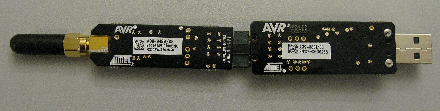
FCC Part 15 & RSS-210 Project no.: 140235 Page 1 of 2 Nemko AS, NO-2007 Kjeller INTERNAL PHOTOS A09-0490 Rear view Top view FCC Part 15 & RSS-210 Project no.: 140235 Page 2 of 2 Nemko AS, NO-2007 Kjeller Whip antenna
Internal Photos
FCC Part 15 & RSS-210 Project no.: 140235 Page 1 of 2 Nemko AS, NO-2007 Kjeller INTERNAL PHOTOS A09-0490 Rear view Top view FCC Part 15 & RSS-210 Project no.: 140235 Page 2 of 2 Nemko AS, NO-2007 Kjeller Whip antenna
Operational Description
Features •High Performance RF-CMOS 2.4 GHz Radio Transceiver Targeted for IEEE 802.15.4 ™ , ZigBee ® , 6LoWPAN, RF4CE, SP100, WirelessHART ™ and ISM Applications •Industry Leading Link Budget (104 dB) – Receiver Sensitivity -101 dBm – Programmable Output Power from -17 dBm up to +3 dBm •Ultra-Low Current Consumption: •Ultra-Low Supply Voltage (1.8V to 3.6V) with Internal Regulator •Optimized for Low BoM Cost and Ease of Production: – Few External Components Necessary (Crystal, Capacitors and Antenna) – Excellent ESD Robustness •Easy to Use Interface: – Registers, Frame Buffer and AES Accessible through Fast SPI – Only Two Microcontroller GPIO Lines Necessary – One Interrupt Pin from Radio Transceiver – Clock Output with Prescaler from Radio Transceiver •Radio Transceiver Features: – 128-byte FIFO (SRAM) for Data Buffering – Programmable Clock Output, to Clock the Host Microcontroller or as Timer Reference – Integrated RX/TX Switch – Fully Integrated, Fast Settling PLL to support Frequency Hopping – Battery Monitor – Fast Wake-Up Time < 0.4 msec •Special IEEE 802.15.4-2006 Hardware Support: – FCS Computation and Clear Channel Assessment – RSSI Measurement, Energy Detection and Link Quality Indication •MAC Hardware Accelerator: – Automated Acknowledgement, CSMA-CA and Retransmission – Automatic Address Filtering – Automated FCS Check •Extended Feature Set Hardware Support: – AES 128-bit Hardware Accelerator – RX/TX Indication (external RF Front-End Control) – RX Antenna Diversity – Supported PSDU data rates: 250 kb/s, 500 kb/s, 1 Mb/s and 2 Mb/s – True Random Number Generation for Security Application •Industrial and Extended Temperature Range: – -40°C to +85°C and -40°C to +125°C •I/O and Packages: – 32-pin Low-Profile QFN Package 5 x 5 x 0.9 mm³ – RoHS/Fully Green •Compliant to IEEE 802.15.4-2006 and IEEE 802.15.4-2003 •Compliant to EN 300 328/440, FCC-CFR-47 Part 15, ARIB STD-T66, RSS-210 – SLEEP = 0.02 μA – TRX_OFF = 0.4 mA – RX_ON = 12.3 mA – BUSY_TX = 14 mA (at max. Transmit Power of +3 dBm) Low Power 2.4 GHz Transceiver for ZigBee, IEEE 802.15.4, 6LoWPAN, RF4CE, SP100, WirelessHART, and ISM Applications AT86RF231-ZU AT86RF231-ZF 8111C–MCU Wireless–09/09 2 8111C–MCU Wireless–09/09 AT86RF231 1. Pin-out Diagram Figure 1-1.AT86RF231 Pin-out Diagram Note:The exposed paddle is electrically connected to the die inside the package. It shall be soldered to the board to ensure electrical and thermal contact and good mechanical stability. 32 24 23 22 21 20 19 18 17 1 2 3 4 5 6 7 8 AT86RF231 CLKM DVSS DIG3 DIG4 AVSS AVSS RFP RFN DVSS /R S T DIG1DIG2 SLP_TR DVSS DVD DDVD D DEVD D DVSS SCLK MISO DVSS MOSI /SEL IR Q XTAL2XTAL1AVSSEVDDAVDDAVSSAVSSAVSS 31 30 29 28 27 26 25 9 10111213141516 AVSS exposed paddle 3 8111C–MCU Wireless–09/09 AT86RF231 1.1Pin Descriptions Table 1-1.Pin Description AT86RF231 PinsNameTypeDescription 1DIG3Digital output (Ground) 1. RX/TX Indicator, see Section 11.5 2. If disabled, pull-down enabled (AVSS) 2DIG4Digital output (Ground) 1. RX/TX indicator (DIG3 inverted), see Section 11.5 2. If disabled, pull-down enabled (AVSS) 3AVSSGroundGround for RF signals 4RFPRF I/ODifferential RF signal 5RFNRF I/ODifferential RF signal 6AVSSGroundGround for RF signals 7DVSSGroundDigital ground 8/RSTDigital inputChip reset; active low 9DIG1Digital output (Ground) 1. Antenna Diversity RF switch control, see Section 11.4 2. If disabled, pull-down enabled (DVSS) 10DIG2Digital output (Ground) 1. Antenna Diversity RF switch control (DIG1 inverted), see Section 11.4 2. Signal IRQ_2 (RX_START) for RX Frame Time Stamping, see Section 11.6 3. If functions disabled, pull-down enabled (DVSS) 11SLP_TRDigital inputControls sleep, transmit start, receive states; active high, see Section 6.5 12DVSSGroundDigital ground 13DVDDSupplyRegulated 1.8V voltage regulator; digital domain, see Section 9.4 14DVDDSupplyRegulated 1.8V voltage regulator; digital domain, see Section 9.4 15DEVDDSupplyExternal supply voltage; digital domain 16DVSSGroundDigital ground 17CLKMDigital outputMaster clock signal output; low if disabled, see Section 9.6 18DVSSGroundDigital ground 19SCLKDigital inputSPI clock 20MISODigital outputSPI data output (Master Input Slave Output) 21DVSSGroundDigital ground 22MOSIDigital inputSPI data input (Master Output Slave Input) 23/SELDigital inputSPI select, active low 24IRQDigital output 1. Interrupt request signal; active high or active low; configurable 2. Frame Buffer Empty Indicator; active high, see Section 11.7 25XTAL2Analog inputCrystal pin, see Section 9.6 26XTAL1Analog inputCrystal pin or external clock supply, see Section 9.6 27AVSSGroundAnalog ground 28EVDDSupplyExternal supply voltage, analog domain 4 8111C–MCU Wireless–09/09 AT86RF231 29AVDDSupplyRegulated 1.8V voltage regulator; analog domain, see Section 9.4 30AVSSGroundAnalog ground 31AVSSGroundAnalog ground 32AVSSGroundAnalog ground PaddleAVSSGroundAnalog ground; Exposed paddle of QFN package Table 1-1.Pin Description AT86RF231 (Continued) PinsNameTypeDescription 5 8111C–MCU Wireless–09/09 AT86RF231 1.2Analog and RF Pins 1.2.1Supply and Ground Pins EVDD, DEVDD EVDD and DEVDD are analog and digital supply voltage pins of the AT86RF231 radio transceiver. AVDD, DVDD AVDD and DVDD are outputs of the internal 1.8V voltage regulators. The voltage regulators are controlled independently by the radio transceivers state machine and are activated dependent on the current radio transceiver state. The voltage regulators can be configured for external supply. For details, refer to Section 9.4 “Voltage Regulators (AVREG, DVREG)” on page 110. AVSS, DVSS AVSS and DVSS are analog and digital ground pins respectively. The analog and digital power domains should be separated on the PCB. 1.2.2RF Pins RFN, RFP A differential RF port (RFP/RFN) provides common-mode rejection to suppress the switching noise of the internal digital signal processing blocks. At board-level, the differential RF layout ensures high receiver sensitivity by rejecting any spuri…
Text truncated - open the document above for the full version.
Operational Description
100 8111C–MCU Wireless–09/09 AT86RF231 tain LQI value. Since the packet error rate is a statistical value, the PER shown in Section 8-6 “Conditional Packet Error Rate versus LQI” on page 99 is based on a huge number of transac- tions. A reliable estimation of the packet error rate cannot be based on a single or a small number of LQI values. 8.6.2Request an LQI Measurement The LQI byte can be obtained after a frame has been received by the radio transceiver. One additional byte is automatically attached to the received frame containing the LQI value. This information can also be read via Frame Buffer read access, see Section 6.2.2 “Frame Buffer Access Mode” on page 20. The LQI byte can be read after IRQ_3 (TRX_END) interrupt. 8.6.3Data Interpretation According to IEEE 802.15.4 a low LQI value is associated with low signal strength and/or high signal distortions. Signal distortions are mainly caused by interference signals and/or multipath propagation. High LQI values indicate a sufficient high signal power and low signal distortions. Note, the received signal power as indicated by received signal strength indication (RSSI) value or energy detection (ED) value of the AT86RF231 do not characterize the signal quality and the ability to decode a signal. As an example, a received signal with an input power of about 6 dB above the receiver sensitiv- ity likely results in a LQI value close to 255 for radio channels with very low signal distortions. For higher signal power the LQI value becomes independent of the actual signal strength. This is because the packet error rate for these scenarios tends towards zero and further increased signal strength, i.e. increasing the transmission power does not decrease the error rate any fur- ther. In this case RSSI or ED can be used to evaluate the signal strength and the link margin. ZigBee networks often require the identification of the "best" routing between two nodes. Both, the LQI and the RSSI/ED can be used for this, dependent on the optimization criteria. If a low packet error rate (corresponding to high throughput) is the optimization criteria then the LQI value should be taken into consideration. If a low transmission power or the link margin is the optimization criteria then the RSSI/ED value is also helpful. Combinations of LQI, RSSI and ED are possible for routing decisions. As a rule of thumb RSSI and ED values are useful to differentiate between links with high LQI values. Transmission links with low LQI values should be discarded for routing decisions even if the RSSI/ED values are high. This is because RSSI/ED does not say anything about the possibility to decode a signal. It is only an information about the received signal strength whereas the source can be an interferer. 101 8111C–MCU Wireless–09/09 AT86RF231 9. Module Description 9.1Receiver (RX) 9.1.1Overview The AT86RF231 receiver is split into an analog radio front end and a digital base band proces- sor (RX BBP), see Figure 9-1 on page 101. Figure 9-1.Receiver Block Diagram The differential RF signal is amplified by a low noise amplifier (LNA), filtered (PPF) and down converted to an intermediate frequency by a mixer. Channel selectivity is performed using an integrated band pass filter (BPF). A limiting amplifier (Limiter) provides sufficient gain to over- come the DC offset of the succeeding analog-to-digital converter (ADC) and generates a digital RSSI signal. The ADC output signal is sampled and processed further by the digital base band receiver (RX BBP). The RX BBP performs additional signal filtering and signal synchronization. The frequency offset of each frame is calculated by the synchronization unit and is used during the remaining receive process to correct the offset. The receiver is designed to handle frequency and symbol rate devi- ations up to ±120 ppm, caused by combined receiver and transmitter deviations. For details refer to Section 12.5 “General RF Specifications” on page 158 parameter 12.5.8. Finally the sig- nal is demodulated and the data are stored in the Frame Buffer. In Basic Operating Mode, refer to Section 7.1 “Basic Operating Mode” on page 33, the reception of a frame is indicated by an interrupt IRQ_2 (RX_START). Accordingly its end is signalized by an interrupt IRQ_3 (TRX_END). Based on the quality of the received signal a link quality indica- tor (LQI) is calculated and appended to the frame, refer to Section 8.6 “Link Quality Indication (LQI)” on page 99. Additional signal processing is applied to the frame data to provide further status information like ED value (register 0x07, ED_LEVEL) and FCS correctness (register 0x06, PHY_RSSI). Beyond these features the Extended Operating Mode of the AT86RF231 supports address filter- ing and pending data indication. For details refer to Section 7.2 “Extended Operating Mode” on page 47. LNAPPFBPFLimiterADC AGC RSSI RFP RFN Analog DomainDigital Domain SPIRX BBP Frame Buffer LO Control, Registers SPI I/F μC I/F 102 8111C–MCU Wireless–09/09 AT86RF231 9.1.2Frame Receive Procedure The frame receive procedure including the radio transceiver setup for reception and reading PSDU data from the Frame Buffer is described in Section 10.1 “Frame Receive Procedure” on page 126. 9.1.3Configuration In Basic Operating Mode the receiver is enabled by writing command RX_ON to register bits TRX_CMD (register 0x02, TRX_STATE) in states TRX_OFF or PLL_ON. Similarly in Extended Operating Mode, the receiver is enabled for RX_AACK operation from states TRX_OFF or PLL_ON by writing the command RX_AACK_ON. There is no additional configuration required to receive IEEE 802.15.4 compliant frames when using the Basic Operating Mode. However, the frame reception in the Extended Operating Mode requires further register configurations, for details refer to Section 7.2 “Extended Operating Mode” on page 47. The AT86RF231 receiver has an outstanding sensitivity performance of -101 dBm. At certain environmental conditions or for High Data Rate Mode…
Text truncated - open the document above for the full version.
Operational Description
Tekfun Co., Ltd. ________________________________________________________________________________________________________________________________________________________________________________________________________________________________ ___ TEKFUN CO., Ltd. E-mail: [email protected] URL: www.tekfun.com.tw 4F., No.32, Kunming St., Jhongli City, Taoyuan Hsien 32089, Taiwan Tel : 886-3-4280826 Fax:886-3-4280010 SPECIFICATION FOR APPROVAL CUSTOMER DESCRIPTION 2.4GHz Rubber Stubby Antenna with SMA Male Straight PART NO. M01-SS2 DATE DESIGNER DIRECTOR Approved by Customer/date: Tekfun Co., Ltd. Page1 of 6 ________________________________________________________________________________________________________________________________________________________________________________________________________________________________ ___ TEKFUN CO., Ltd. E-mail: [email protected] URL: www.tekfun.com.tw 4F., No.32, Kunming St., Jhongli City, Taoyuan Hsien 32089, Taiwan Tel : 886-3-4280826 Fax:886-3-4280010 ANTENNA SPECIFICATIONS FOR APPROVAL 1. GENERAL DESCRIPION 1.1 Type No. : M01-SS2 1.2 Customer P/N : 2. DESCRIPTION & APPLICATION 2.4GHz Rubber Stubby Antenna with SMA Male Straight 3. ELECTRICAL CHARACTERISTICS 3.1 Frequency Range : 2.4GHz (2.4~2.5GHz) 3.2 Electric Wave : 1/4, Monopole Antenna 3.3 V.S.W.R : < 2 3.4 Impedance : 50 Ω, Nominal 3.5 Gain : < 0dBi 3.6 Connector : SMA Male Straight 4. PACKING STYLE Poly Bag Tekfun Co., Ltd. ________________________________________________________________________________________________________________________________________________________________________________________________________________________________ ___ TEKFUN CO., Ltd. E-mail: [email protected] URL: www.tekfun.com.tw 4F., No.32, Kunming St., Jhongli City, Taoyuan Hsien 32089, Taiwan Tel : 886-3-4280826 Fax:886-3-4280010 5. APPEARANCE DRAWING Tekfun Co., Ltd. ________________________________________________________________________________________________________________________________________________________________________________________________________________________________ ___ TEKFUN CO., Ltd. E-mail: [email protected] URL: www.tekfun.com.tw 4F., No.32, Kunming St., Jhongli City, Taoyuan Hsien 32089, Taiwan Tel : 886-3-4280826 Fax:886-3-4280010 6. Test Report VSWR Tekfun Co., Ltd. ________________________________________________________________________________________________________________________________________________________________________________________________________________________________ ___ TEKFUN CO., Ltd. E-mail: [email protected] URL: www.tekfun.com.tw 4F., No.32, Kunming St., Jhongli City, Taoyuan Hsien 32089, Taiwan Tel : 886-3-4280826 Fax:886-3-4280010 7. Test Report Return LOSS
Parts List/Tune Up Info
Qty Designator Description MPN Manufacturer ShortName 1 C105 Ceramic capacitor, SMD 0402, NP0, 50V, +/-0.25pF 1.5p 2 C103, C104 Ceramic capacitor, SMD 0402, NP0, 50V, +/-5% 12p 1 C111 Ceramic capacitor, SMD 0402, X7R, 25V, +/-10% 10n 1 C110 Ceramic capacitor, SMD 0402, X7R, 16V, +/-10% C0402C104K4RACTU Kemet 100n 9 C101, C102, C106, C107, C108, C109, C112, C113, C114 Ceramic capacitor, SMD 0402, X5R, 6.3V, +/-10% C0402C105K9PAC Kemet 1u 4 R102, R104, R105, R109 Thick film resistor, SMD 0402, 1/16W, 1% 0R 1 R106 Thick film resistor, SMD 0402, 1/16W, 1% 470R 1 R111 Thick film resistor, SMD 0402, 1/16W, 1% 2.2k 1 L101 SMD RF inductor 0805. Z=1000Ohm (@100MHz), Max R(dc)=0.45Ohm, Max current=200mA BLM21AG102SN1D Murata BLM21AG102SN1D 1 L102 2,4 - 2,5GHZ FilterBalun, 2x1,25mm 2450FB15L0001E Johanson Technology 2,4GHz FilterBalun 1 U101 2.4GHz ZigBee/802.15.4 tranceiver AT86RF231-ZU ATMEL AT86RF231-ZU 1 U103 1-wire Serial number chip DS2411R/T&R Maxim DS2411R 1 U102 LDO 3.3V 150mA SOT23-5 LP2985AIM5-3.3 National Semiconductor LP2985 3.3V 1 XC101 SMT Crystal Resonator, 16.000 MHz,10 ppm,12 pF, 2520(Q) SCQ18D48-16.000MHZ TR SUNTSU FREQUENCY CONTROL 16MHz 1 J101 Samtec SMH 2x5 Pin Socet Right-angle 2,54mm Pitch (Mirrored footprint) SMH-105-02-T-D-TR SAMTEC SMH-105-02-T-D-TR 1 PCB101 RZ600 RF board PCB NCAB RZ600 RF board PCB 1 J102 SMA PCB mounted connector LTI-SASF56GT Lighthorse Technologies inc. LTI-SASF56GT 1 Z102 Label for use on wireless PCBA that needs 64 bit MAC and FCC ID 505462 ACT Logimark AS Label PCBA with MAC64 and FCC ID 1 PCBA101 RZ600 RF board PCBA RZ600 RF board PCBA
Schematics
1 1 2 2 3 3 4 4 5 5 6 6 7 7 8 8 DD CC BB AA A12-0171 A08-0671 Rev3.SchDoc 111/8/20101:00:05 PM RF Board Embedded Wireless Labs Sdn Bhd 702, Uptown 2, SS21/37 Damansara Uptown PJ, Sel, Malaysia PAGE:of TITLE: Document number:Revision:Rev 3 Date: Jeyaraman * * 12 34 56 78 910 SMH-105-02-T-D-TR J101 AVSS 1 AVSS 2 AVSS 3 RFP 4 RFN 5 AVSS 6 TST 7 RST 8 DVSS 9 DVSS 10 SLP_TR 11 DVSS 12 DVDD 13 DVDD 14 DEVDD 15 DVSS 16 CLKM 17 DVSS 18 SCLK 19 MISO 20 DVSS 21 MOSI 22 SEL 23 IRQ 24 XTAL1 25 XTAL2 26 AVSS 27 EVDD 28 AVDD 29 AVSS 30 AVSS 31 AVSS 32 AVSS 33 U101 AT86RF230-ZU UnBal 1 GND 2 BAL1 3 BAL2 4 GND 5 GND/NC 6 L102 2450FB15L0001 10K R104 1 2 3 CD75014 1X3 J104 1 24 3 SCQ18D48-16.000MHz TR XC101 I/O 1 VCC 2 GND 3 U103 DS2411-R RF_VCC 12pF C104 12pF C103 1uF C101 1uF C102 1uF C112 1uF C113 RF_VCC VCC 1uF C114 VCC 2.2K R111 VCC IRQ SEL MOSI MISO SCLK CLKM 1uF C106 100nF C110 RSTRST SLP_TR RST IRQ SEL MISO SLP_TR MOSI SCLK 12 CD075014 1X2 J103 RF_VCC TST ID LTI-SASF56GT RF 1 GND 2 GND 3 J102 0R / NM R108 0R R109 0R / NM R110 MISC MISC Private & Confidential BLM21AG102SN1D L1010R R105 470R R106 0R / NM R107 0R / NM R103 0R / NM R101 1.5pF C105 L102: For RF212: Use P/N 0896FB15A0100E, Johanson Technology U101: For RF212: Use P/N AT86RF212-ZU, Atmel For RF231: Use P/N AT86RF231-ZU, Atmel 1uF C107 1uF C108 1uF C109 R104: For RF212: Use 0R Value For RF231: Use 0R Value R102: For RF212: Use 100pF Capacitor 0R R102 PCB101 A08-0671 GND 2 GND 1 GND 3 GND 4 Z101 Z102 PCBA Label Place Label on the Bottom Side Place EMI Shield on Top Side IN 1 OUT 5 2 BYP 4 ON/OFF 3 GND LP2985AIM5-3.3/NOPB U102 10nF C111 TP112 TP104TP105 TP109 TP113 TP110 TP101 TP102 TP107TP111TP108TP106 RF_P RF_N A a i PCB Rule i PCB Rule i PCB Rule i PCB Rule TP114 MISC RST SLP_TR MISC CLKM TP115 0R / NM R112 R101, R103, R107, R112 Equip for RF230 Do not Equip for RF231 & RF212 TP116TP117TP118TP119TP120TP121TP122 SCLKMOSISLP _TR SEL MISOIRQ RST TP123 MISC Transciever Current Measurement: Mount J103 & Remove R105 PIC10101PIC10102 COC101 PIC10201PIC10202 COC102 PIC10301 PIC10302 COC103 PIC10401 PIC10402 COC104 PIC10501 PIC10502 COC105 PIC10601 PIC10602 COC106 PIC10701 PIC10702 COC107 PIC10801 PIC10802 COC108 PIC10901 PIC10902 COC109 PIC11001 PIC11002 COC110 PIC11101 PIC11102 COC111 PIC11201 PIC11202 COC112 PIC11301 PIC11302 COC113 PIC11401 PIC11402 COC114 PIJ10101PIJ10102 PIJ10103PIJ10104 PIJ10105PIJ10106 PIJ10107PIJ10108 PIJ10109PIJ101010 COJ101 PIJ10201 PIJ10202 PIJ10203 COJ102 PIJ10301PIJ10302 COJ103 PIJ10401 PIJ10402 PIJ10403 COJ104 PIL10101PIL10102 COL101 PIL10201 PIL10202 PIL10203 PIL10204 PIL10205PIL10206 COL102 COPCB101 PIR10101PIR10102 COR101 PIR10201PIR10202 COR102 PIR10301PIR10302 COR103 PIR10401 PIR10402 COR104 PIR10501PIR10502 COR105 PIR10601 PIR10602 COR106 PIR10701 PIR10702 COR107 PIR10801 PIR10802 COR108 PIR10901 PIR10902 COR109 PIR11001 PIR11002 COR110 PIR11101 PIR11102 COR111 PIR11201 PIR11202 COR112 PITP10101 COTP101 PITP10201 COTP102 PITP10401 COTP104 PITP10501 COTP105 PITP10601 COTP106 PITP10701 COTP107 PITP10801 COTP108 PITP10901 COTP109 PITP11001 COTP110 PITP11101 COTP111 PITP11201 COTP112 PITP11301 COTP113 PITP11401 COTP114 PITP11501 COTP115 PITP11601 COTP116 PITP11701 COTP117 PITP11801 COTP118 PITP11901 COTP119 PITP12001 COTP120 PITP12101 COTP121 PITP12201 COTP122 PITP12301 COTP123 PIU10101 PIU10102 PIU10103 PIU10104 PIU10105 PIU10106 PIU10107 PIU10108 PIU10109PIU101010PIU101011PIU101012PIU101013PIU101014PIU101015PIU101016 PIU101017 PIU101018 PIU101019 PIU101020 PIU101021 PIU101022 PIU101023 PIU101024 PIU101025PIU101026PIU101027PIU101028PIU101029PIU101030PIU101031PIU101032PIU101033 COU101 PIU10201 PIU10202 PIU10203PIU10204 PIU10205 COU102 PIU10301PIU10302 PIU10303 COU103 PIXC10101 PIXC10102 PIXC10103 PIXC10104 COXC101 PIZ10101PIZ10102PIZ10103PIZ10104 COZ101 COZ102 PIC10501 PIJ10401 PIR10601 PIR11001 NLCLKM PIC10101 PIC10201 PIC10302PIC10402 PIC10502 PIC10602PIC10702PIC10802PIC10902PIC11002 PIC11102 PIC11201PIC11301 PIC11401 PIJ10109 PIJ10202 PIJ10203 PIL10202PIL10205PIL10206 PIR10102 PIR10302 PIR10401 PIR10701 PIR11201 PITP11201 PITP11401 PIU10103 PIU10106 PIU101012PIU101016 PIU101018 PIU101021 PIU101027PIU101030PIU101031PIU101032PIU101033 PIU10202 PIU10303 PIZ10101PIZ10102PIZ10103PIZ10104 PIJ10402 PIR10901 PIR11101 PIU10301 NLID PIJ10103 PITP11701 PIU101024 NLIRQ PIJ10102 PIR10802PIR10902PIR11002 PITP12301 NLMISC PIJ10107 PITP12101 PIU101020 NLMISO PIJ10106 PITP12001 PIU101022 NLMOSI PIC10202 PITP10201 PIU101029 PIC10301 PIU101025 PIXC10101 PIC10401 PIU101026 PIXC10103 PIC10601 PIJ101010 PITP10701 PIU10201 PIU10203 PIC11101 PITP11101 PIU10204 PIC11202 PITP11301 PIU101013PIU101014 PIJ10201PIR10202 PIJ10301 PIL10101 PIR10502 PITP10601 PIL10201PIR10201 PIR10101 PITP10401 PIU10101 PIR10301 PITP10501 PIU10102 PIR10602 PITP11001 PIU101017 PIR10702 PITP10901 PIU10109 PIR11202 PITP11501 PIU101010 PIXC10102PIXC10104 PIJ10101 PITP11601 PIU10108 NLR\S\T\ PIL10203 PIU10105 NLRF0N PIL10204 PIU10104 NLRF0P PIC10102 PIC11302 PIL10102 PITP10101 PIU101015 PIU101028 PIJ10105 PITP11901 PIU101023 NLS\E\L\ PIJ10108 PITP12201 PIU101019 NLSCLK PIJ10104 PITP11801 PIU101011 NLSLP0TR PIJ10403 PIR10402 PIR10801 PIU10107 NLTST PIC10701PIC10801PIC10901PIC11001 PIC11402 PIJ10302 PIR10501 PIR11102 PITP10801 PIU10205 PIU10302
Schematics
1 1 2 2 3 3 4 4 5 5 6 6 7 7 8 8 DD CC BB AA A12-0172 A08-0672 Rev3.SchDoc 111/8/201012:57:53 PM USB Adaptor Embedded Wireless Labs Sdn Bhd 702, Uptown 2, SS21/37 Damansara Uptown, PJ, Sel, Malaysia PAGE:of TITLE: Document number:Revision:Rev 3 Date: Jeyaraman * * USB_P USB_N PA0 G11 PA1 G12 PA2 D8 PA3 G10 PA4 F9 PA5 F10 PA6 F8 PA7 E10 PA8 C11 PA9 B12 PA10 C12 PA11 D10 PA12 E12 PA13 F11 PA14 J6 PA15 J7 PA16 F12 PA17 H7 PA18 K8 PA19 J8 PA20 J9 PA21 H9 PA22 H10 PA23 G8 PA24 G9 PA25 E9 PA26 D9 PA27 A4 PA28 A3 PA29 A6 PA30 C7 PC0/XIN32 K5 PC1/XOUT32 H6 PC2/XIN0 A7 PC3/XOUT0 B7 PC4/XIN1 A8 PC5/XOUT1 A9 PA31 B3 FSDM B10 FSDP C9 HSDM A11 HSDP A10 VBUS A12 VBIAS B9 RESET_N J12 TCK K12 TDO J11 TDI L12 TMS J10 VDDCORE E11 ONREG L8 VDDIN E8 GNDCORE C10 GNDPLL B11 VDDANA H11 GNDANA L11 VDDIO E2 GNDIO C3 VDDIO H2 GNDIO L2 VDDIO B5 GNDIO K3 VDDIO E5 GNDIO F6 GNDIO G6 VDDIO H5 VDDIO/VBOOST H8 GNDIO F7 VDDIO L5 GNDIO G7 GNDIO K10 VDDIO B8 PX0 G1 PX1 H1 PX2 J2 PX3 K1 PX4 J1 PX5 G2 PX6 F3 PX7 F2 PX8 D1 PX9 C1 PX10 B1 PX11 L1 PX12 D6 PX13 C6 PX14 M4 PX15 E6 PX16 C5 PX17 K6 PX18 L6 PX19 D5 PX20 L4 PX21 M5 PX22 M1 PX23 M6 PX24 M7 PX25 M8 PX26 L9 PX27 K9 PX28 L10 PX29 K11 PX30 M11 PX31 M10 PX32 M9 PX33 M12 PX34 J3 PX35 C2 PX36 D3 PX37 D2 PX38 E1 PX39 F1 PX40 A1 PX41 M2 PX42 M3 PX43 L7 PX44 K2 PX45 L3 PX46 K4 PX47 D4 PX48 F5 PX49 F4 PX50 G4 PX51 G5 PX52 K7 PX53 E4 PX54 E3 PX55 J5 PX56 J4 PX57 H4 PX58 H3 PX59 G3 PB0 A2 PB1 C4 PB2 B4 PB3 A5 PB4 B6 PB5 H12 PB6 D12 PB7 D11 PB8 C8 PB9 E7 PB10 D7 PB11 B2 U101 AT32UC3A3256S 10K R101 1uF C105 VCC RESET_N USB_P USB_N 6810R R102 VUSB VUSB 12 34 56 78 910 STL21-0730 G TT-10U J103 TCK TDO TMS TDI 1uF C111 VCC 12pF C104 12p…
Text truncated - open the document above for the full version.
Contact Information
Applicant
Steve Caldwell(Vice President, Wireless Solutions Group)
Test Firm
Nemko ASFrode Sveinsen
Technical Specifications
| # | Rule Parts | Frequency Range | Power Output |
|---|---|---|---|
| 1 | 15C | 2.40 GHz - 2.48 GHz | 530.00 µW |
Other Applications from Microchip Technology Inc.
VW4A091980
Dec 22, 2015ATREB215-XPRO
Equipment Class
DXX - Part 15 Low Power Communication Device TransmitterVW4A092412
Mar 27, 2015ATSAMR21ZLL-EK
Equipment Class
DTS - Digital Transmission System
VW4A091982
Mar 21, 2015ATREB215-XPRO
Equipment Class
DTS - Digital Transmission System
VW4ATWILC1000
Dec 03, 2014Wireless Module
Equipment Class
DTS - Digital Transmission System
VW4ATWINC1500
Nov 17, 2014Wireless Module
Equipment Class
DTS - Digital Transmission System