VW4A09-0743ATMEGA128RFA1-EK1
Microchip Technology Inc.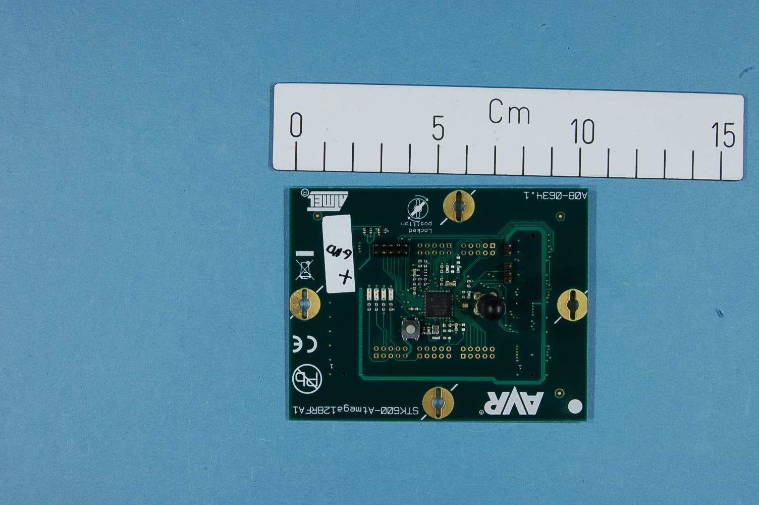
Click to zoom
Application Details
- Equipment Class
- DTS - Digital Transmission System
- Date of Grant
- Mar 17, 2010
- Application Purpose
- Original Equipment
- Date of Application
- Mar 16, 2010
- Equipment Note
- ATMEGA128RFA1-EK1
- Frequency Range
- 2405.00000000 - 2480.00000000
- Company
- Microchip Technology Inc.
- Country
- United States
Documents & Files
Document Text
Text extracted from the exhibit documents filed with the FCC. Open a document above to read the original.
Users Manual
RCB Certification Firmware Manual Features • User Manual for RCB Certification Firmware 1 Introduction The manual describes the usage of RCB (DUT) firmware for certification purposes. Figure 1-1 as an example shows one target board demonstrating the 8 bit AVR microcontroller with integrated low power 2.4 GHz transceiver [1]. Figure 1-1. RCB128RFA1 – Single-Chip Radio Controller Board Other DUTs may look different with a slightly different user interface, for details refer to section 2. RCB Certification Firmware Manual Rev. 0001B-AVR-10/09 2 AVR0000 0001B-AVR-10/09 2 Hardware Description 2.1 RCB128RFA1 v6.3.1 The RCB features the following user interface: • (3) STATUS LED’s (LED_0 ... LED_2) • (1) RESET LED (LED_R) • (1) Push Button (Button) • (1) Power Switch (Sw) Figure 2-1. RCB128RFA1 v6.3.1 – User Interface Main components: • 8 bit AVR microcontroller with integrated low power 2.4 GHz transceiver [1] • AT25010A, EEPROM • Antenna, Mobile Mark PSTG0-2400HS Figure 1-1 shows the RCB without shielding cover in an active state, the microcontroller part is running and the radio transceiver part is in TRX_OFF state (IDLE / Standby). For details refer to the next sections. The RCB is manufactured, tested and shipped with shielding cover attached to the frame. AVR0000 3 0001B-AVR-10/09 2.2 RCB231 v4.0.2 The RCB features the following user interface: • (3) STATUS LED’s (LED_0 ... LED_2) • (1) Push Button (Button) • (1) Power Switch (Sw) Figure 2-2. RCB231 v4.0.2 – User Interface Main components: • AT86RF231, 2.4 GHz low power radio transceiver [2] • ATmega1281, 8 bit AVR microcontroller • AT25010A, EEPROM • Antenna, on board or antenna connector The picture shows the RCB in an active state, the microcontroller part is running and the radio transceiver part is in TRX_OFF state (IDLE / Standby). For details refer to the next sections. Note the different order or weighting of the LED’s compared to the RCB shown in 2.1. 4 AVR0000 0001B-AVR-10/09 2.3 RCB231LPA v4.3.2 The RCB features the following user interface: • (3) STATUS LED’s (LED_0 ... LED_2) • (1) Push Button (Button) • (1) Power Switch (Sw) Figure 2-3. RCB231LPA v4.3.2 – User Interface Main components: • AT86RF231, 2.4 GHz low power radio transceiver [2] • uPG2314T5N, Power Amplifier • ATmega1281, 8 bit AVR microcontroller • AT25010A, EEPROM • Antenna, Mobile Mark PSTG0-2400HS The picture shows the RCB in OFF state. Note the different order or weighting of the LED’s compared to the RCB shown in 2.1. Figure 2-3 shows the RCB for illustration without shielding cover. However, the board is manufactured, tested and shipped with shielding attached to the frame. AVR0000 5 0001B-AVR-10/09 2.4 RCB212SMA v5.3.2 To be defined, no firmware support yet. 6 AVR0000 0001B-AVR-10/09 3 Firmware Description 3.1 Prerequisites Before power-on the DUT by moving (Sw) to (ON) position, ensure the DUT is equipped with two AAA batteries. These batteries are to be placed at the back side of the DUT in the battery holder. Pay attention to the correct polarity of the batteries. 3.2 Power-On and Configuration There are two possibilities to power-on the DUT: 1. Without DUT configuration update, 2. Configuration mode (press (Button) during power-on). The next sections describe different ways to power-on a DUT in detail. 3.2.1 Without DUT Configuration Update The first choice is the standard selection to power-on the DUT. To select operation without radio transceiver configuration update, power-on the DUT by switching (Sw) to (ON) position. Do not press the (Button). There are two possible system configurations: • The very first power-on cycle (factory reset) enables operation at maximum TX output power and standard PSDU data rate. The DUT starts at test mode state “0”, refer to section 3.3. • All other power-on cycles remember the last radio transceiver configuration and test mode selection before last power-off cycle. If available, the LED indicating the reset state (LED_R) is on for a short time. Once this LED is off again, the microcontroller is waiting for a new (Button) command. 3.2.2 Configuration Mode Power-on the DUT in configuration mode allows either: • Reset to factory configuration, and, if required • Selection of TX output power and/or PSDU data rate, see references [1...2]. To do this, press and hold the (Button) before power-up the DUT. Once the DUT is powered on, the three state LED’s (LED_0 ... LED_2) are switched on. Further handling of the (Button) determines the next configuration options. 3.2.2.1 Factory Reset If the (Button) is pressed during power-on and immediately released afterwards, factory reset configuration is loaded. If TX output power has to be switched to the minimum value do not release the (Button) within two seconds, for details refer to 3.2.2.2. AVR0000 7 0001B-AVR-10/09 If no further (Button) activity is recognized, all three state LED’s are switched off 5 sec later. Continue to select the test mode as described in section 3.3. 3.2.2.2 Transmitter Output Power Selection If the (Button) is not released for about two seconds after power-on, the TX output power is set to the minimum possible value. This is indicated by switching off the three state LED’s (LED_0 ... LED_2), and immediately after switching on state LED (LED_2). Now the (Button) has to be released to continue with PSDU data rate selection, or wait to leave the radio transceiver configuration menu 5 sec later. PSDU Data Rate Selection Release the (Button) either immediately or after TX output power selection, to enable the PSDU rate selection. This is possible independently on a previous TX output configuration. Each new (Button) press toggles the status LED’s similar to a binary counter between 1 through 4. Note, a new (Button) press event to select the PSDU data rate has to be performed within 5 sec after power-on or TX output power selection. Otherwise the configuration menu is left towards the Test Mode Selection, see section 3.3. The PSDU data rate is coded as follow: …
Text truncated - open the document above for the full version.
Block Diagram
Radio chip ATmega128RFA1 GPIO interface 16MHz Xtal MCU oscillator Antenna M01-SS2 32kHz Xtal Realtime Clock oscillator SMA connector Block Diagram, ATmega128RFA1-EK1, A09-0743
Internal Photos
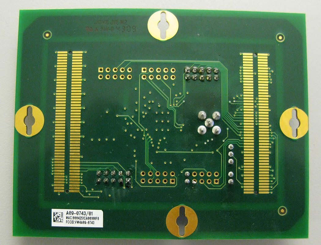
FCC Part 15 & RSS-210 Project no.: 140235 Page 1 of 2 Nemko AS, NO-2007 Kjeller INTERNAL PHOTOS 128RFA1 Top view Rear view FCC Part 15 & RSS-210 Project no.: 140235 Page 2 of 2 Nemko AS, NO-2007 Kjeller Whip antenna
Operational Description
1 8266A-MCU Wireless-12/09 ATmega128RFA1 8-bit Microcontroller with Low Power 2.4GHz Transceiver for ZigBee and IEEE 802.15.4 ATmega128RFA1 PRELIMINARY 8266A-MCU Wireless-12/09 Features • High Performance, Low Power AVR ® 8-Bit Microcontroller • Advanced RISC Architecture - 135 Powerful Instructions – Most Single Clock Cycle Execution - 32x8 General Purpose Working Registers - Fully Static Operation - Up to 16 MIPS Throughput at 16 MHz and 1.8V - On-Chip 2-cycle Multiplier • Non-volatile Program and Data Memories - 128K Bytes of In-System Self-Programmable Flash • Endurance: 2000 Write/Erase Cycles @ 85°C - 4K Bytes EEPROM • Endurance: 2000 Write/Erase Cycles @ 85°C - 16K Bytes Internal SRAM • JTAG (IEEE std. 1149.1 compliant) Interface - Boundary-scan Capabilities According to the JTAG Standard - Extensive On-chip Debug Support - Programming of Flash EEPROM, Fuses and Lock Bits through the JTAG interface • Peripheral Features - Multiple Timer/Counter & PWM channels - Real Time Counter with Separate Oscillator - 10-bit, 330 ks/s A/D Converter; Analog Comparator; On-chip Temperature Sensor - Master/Slave SPI Serial Interface - Two Programmable Serial USART - Byte Oriented 2-wire Serial Interface • Advanced Interrupt Handler • Watchdog Timer with Separate On-Chip Oscillator • Power-on Reset and Low Current Brown-Out Detector • Advanced Power Save Modes • Fully integrated Low Power Transceiver for 2.4 GHz ISM Band - Supported Data Rates: 250 kb/s and 500 kb/s, 1 Mb/s, 2 Mb/s - -100 dBm RX Sensitivity; TX Output Power up to 3.5 dBm - Hardware Assisted MAC (Auto-Acknowledge, Auto-Retry) - 32 Bit IEEE 802.15.4 Symbol Counter - Baseband Signal Processing - SFR-Detection, Spreading; De-Spreading; Framing ; CRC-16 Computation - Antenna Diversity and TX/RX control - TX/RX 128 Byte Frame Buffer • Hardware Security (AES, True Random Generator) • Integrated Crystal Oscillators (32.768 kHz & 16 MHz) • I/O and Package - 38 Programmable I/O Lines - 64-pad QFN (RoHS/Fully Green) • Temperature Range: -40°C to 85°C Industrial • Supply voltage range 1.8V to 3.6V with integrated voltage regulators • Ultra Low Power consumption (1.8 to 3.6V) for Rx/Tx & AVR: <18.6 mA - CPU Active Mode (16MHz): 4.1 mA - 2.4GHz Transceiver: RX_ON 12.5 mA / TX 14.5 mA (maximum TX output power) - Deep Sleep Mode: <250nA @ 25°C • Speed Grade: 0 – 16 MHz @ 1.8 – 3.6V Applications • ZigBee ® / IEEE 802.15.4-2006/2003™ – Full And Reduced Function Device (FFD/RFD) • General Purpose 2.4GHz ISM Band Transceiver with Microcontroller • RF4CE, SP100, WirelessHART™, ISM Applications and IPv6 / 6LoWPAN 2 8266A-MCU Wireless-12/09 ATmega128RFA1 1 Pin Configurations Figure 1-1. Pinout ATmega128RFA1 Note: The large center pad underneath the QFN/MLF package is made of metal and internally connected to AVSS. It should be soldered or glued to the board to ensure good mechanical stability. If the center pad is left unconnected, the package might loosen from the board 2 Disclaimer Typical values contained in this datasheet are based on simulation and characterization results of other AVR microcontrollers and radio transceivers manufactured in a similar process technology. Minimum and Maximum values will be available after the device is characterized. 1 [PF3:ADC3:DIG4] [PF2:ADC2:DIG2] 2 3 [PF5:ADC5:TMS] [PF4:ADC4:TCK] 4 5 [PF7:ADC7:TDI] [PF6:ADC6:TDO] 6 7 [RFP] [AVSS_RFP] 8 9 [AVSS_RFN] [RFN] 10 11 [RSTN] [TST] 12 13 14 [RSTON] [PG0:DIG3] 56 55 54 53 52 51 62 61 60 59 58 57 64 63 ATmega128RFA1 Exposed paddle: [AVSS] [DVSS] [PE0:RXD0:PCINT8] [PE1:TXD0] [PE2:XCK0:AIN0] [CLKI] [DEVDD] [DVSS] [PB0:SSN:PCINT0] [PB1:SCK:PCINT1] [PB2:MOSI:PDI:PCINT2] [PB3:MISO:PDO:PCINT3] [PB4:OC2A:PCINT4] [PB5:OC1A:PCINT5] [PB6:OC1B:PCINT6] 31 32 17 18 19 20 21 23 22 24 25 26 27 0 28 [PD3:TXD1:INT3] [PD2:RXD1:INT2] [PD1:SDA:INT1] [PD0:SCL:INT0] [DVSS] [DEVDD] [DVDD][DVDD] [DVSS:DSVSS] [PG5:OC0B] [PG4:TOSC1][PG3:TOSC2] [PD7:T0][PD6:T1] 42 41 40 39 38 37 36 35 34 33 48 47 46 45 15 16 [PG1:DIG1] [PG2:AMR] [PB7:OC0A:OC1C:PCINT7] [DEVDD] 44 43 29 0 30 [PD5:XCK1] [PD4:ICP1] 50 49 Index corner [DEVDD] [PE7:ICP3:INT7:CLKO] [PE6:T3:INT6] [PE5:OC3C:INT5] [PE4:OC3B:INT4] [PE3:OC3A:AIN1] [XTAL2] [DVSS] [PF1:ADC1] [PF0:ADC0] [AREF] [AVSS:ASVSS] [AVDD] [EVDD] [AVSS] [XTAL1] 3 8266A-MCU Wireless-12/09 ATmega128RFA1 3 Overview The ATmega128RFA1 is a low-power CMOS 8 bit microcontroller based on the AVR enhanced RISC architecture combined with a high data rate transceiver for the 2.4 GHz ISM band. It is derived from the ATmega1281 microcontroller and the AT86RF231 radio transceiver. By executing powerful instructions in a single clock cycle, the device achieves throughputs approaching 1 MIPS per MHz allowing the system designer to optimize power consumption versus processing speed. The radio transceiver provides high data rates from 250 kb/s up to 2 Mb/s, frame handling, outstanding receiver sensitivity and high transmit output power enabling a very robust wireless communication. 3.1 Block Diagram Figure 3-1 Block Diagram The AVR core combines a rich instruction set with 32 general purpose working registers. All 32 registers are directly connected to the Arithmetic Logic Unit (ALU). Two independent registers can be accessed with one single instruction executed in one clock cycle. The resulting architecture is very code efficient while achieving throughputs up to ten times faster than conventional CISC microcontrollers. The system includes internal voltage regulation and an advanced power management. Distinguished by the small leakage current it allows an extended operation time from battery. The radio transceiver is a fully integrated ZigBee solution using a minimum number of external components. It combines excellent RF performance with low cost, small size and low current consumption. The radio transceiver includes a crystal stabilized fractional-N synthesizer, transmitter and receiver, and full Direct Sequence Spread 4 8266A-MCU Wireless-12/09 ATmega128RFA1 Spectrum Signal (DSSS) process…
Text truncated - open the document above for the full version.
Operational Description
262 8266A-MCU Wireless-12/09 ATmega128RFA1 TCNTn and the OCRnx. Note that when working with fixed TOP values, the unused bits are masked to zero when any of the OCRnx Registers are written. As the third period shown in Figure 18-8 illustrates, changing the TOP actively while the Timer/Counter is running in the phase correct mode can result in an asymmetrical output. The reason for this can be found in the update time of the OCRnx Register. Since the OCRnx update occurs at TOP, the PWM period starts and ends at TOP. This implies that the length of the falling slope is determined by the previous TOP value, while the length of the rising slope is determined by the new TOP value. When these two values are not equal the two slopes of the period will differ in length. The difference in length gives the asymmetrical result of the output. It is recommended to use the phase and frequency correct mode instead of the phase correct mode when changing the TOP value while the Timer/Counter is running. When using a static TOP value there are practically no differences between the two modes of operation. In phase correct PWM mode, the compare units allow generating PWM waveforms on the OCnx pins. Setting the COMnx1:0 bits to 2 will produce a non-inverted PWM. An inverted PWM output can be generated by setting the COMnx1:0 to 3 (see Table 18-4 on page 256). The actual OCnx value will only be visible on the port pin if the data direction of the port pin is set to output (DDR_OCnx). The PWM waveform is generated by setting (or clearing) the OCnx Register at the compare match between OCRnx and TCNTn when the counter increments, and by clearing (or setting) the OCnx Register at compare match between OCRnx and TCNTn when the counter decrements. The PWM frequency of the output f OCnxPCPWM when using phase-correct PWM can be calculated with the following equation: )2 /_ TOPN f f OIclk OCnxPCPWM ⋅⋅ = The N variable represents the prescaler divider (1, 8, 64, 256, or 1024). The extreme values for the OCRnx Register represent special cases when generating a PWM waveform output in the phase correct PWM mode. If the OCRnx is set equal to BOTTOM the output will be continuously low and if set equal to TOP the output will be continuously high for non-inverted PWM mode. For inverted PWM the output will have the opposite logic values. If OCR1A is used to define the TOP value (WGM13:0 = 11) and COM1A1:0 = 1, the OC1A output will toggle with a 50% duty cycle. 18.9.5 Phase and Frequency Correct PWM Mode The phase and frequency correct Pulse Width Modulation (PWM) mode (WGMn3:0 = 8 or 9) provides a high resolution phase and frequency correct PWM waveform generation option. The phase and frequency correct PWM mode is, like the phase correct PWM mode, based on a dual-slope operation. The counter counts repeatedly from BOTTOM (0x0000) to TOP and then from TOP to BOTTOM. In non-inverting Compare Output mode, the Output Compare (OCnx) is cleared on the compare match between TCNTn and OCRnx while up-counting, and set on the compare match while down-counting. In inverting Compare Output mode, the operation is inverted. The dual- slope operation gives a lower maximum operation frequency compared to the single- slope operation. However these modes are preferred for motor control applications due to the symmetric feature of the dual-slope PWM modes. The main difference between the phase correct and the phase and frequency correct PWM mode is the time the OCRnx Register is updated by the OCRnx Buffer Register, (see Figure 18-8 on page 261 and Figure 18-9 on page 263). 263 8266A-MCU Wireless-12/09 ATmega128RFA1 The PWM resolution for the phase and frequency correct PWM mode can be defined by either ICRn or OCRnA. The minimum resolution allowed is 2 bit (ICRn or OCRnA set to 0x0003), and the maximum resolution is 16 bit (ICRn or OCRnA set to MAX). The PWM resolution R PFCPWM in bits can be calculated with the following equation: )2log( )1log(+ = TOP R PFCPWM In phase and frequency correct PWM mode the counter is incremented until the counter value matches either the value in ICRn (WGMn3:0 = 8), or the value in OCRnA (WGMn3:0 = 9). The counter has then reached TOP and changes the count direction. The TCNTn value will be equal to TOP for one timer clock cycle. The timing diagram for the phase correct and frequency correct PWM mode is shown in Figure 18-9 below. The figure shows phase and frequency correct PWM mode when OCRnA or ICRn is used to define TOP. The TCNTn value is shown in the timing diagram as a histogram for illustrating the dual-slope operation. The diagram includes non-inverted and inverted PWM outputs. The small horizontal line marks on the TCNTn slopes represent compare matches between OCRnx and TCNTn. The OCnx Interrupt Flag will be set when a compare match occurs. Figure 18-9. Phase and Frequency Correct PWM Mode Timing Diagram OCRnx/TOP Updateand TOVn Interrupt Flag Set (Interrupt on Bottom) OCnA Interrupt Flag Set or ICFn Interrupt Flag Set (Interrupt on TOP) 1234 TCNTn Period OCnx OCnx (COMnx1:0 = 2) (COMnx1:0 = 3) The Timer/Counter Overflow Flag (TOVn) is set at the timer clock cycle when the OCRnx Registers are updated with the double-buffered value (at BOTTOM). The OCnA or ICFn Flag is set after TCNTn has reached TOP when either OCRnA or ICRn is used for defining the TOP value. The Interrupt Flags can then be used to generate an interrupt each time the counter reaches the TOP or BOTTOM value. When changing the TOP value the program must ensure that the new TOP value is higher or equal to the value of all of the Compare Registers. If the TOP value is lower than any of the Compare Registers, a compare match will never occur between the TCNTn and the OCRnx. As Figure 18-9 shows the output generated is, in contrast to the phase correct mode, symmetrical in all periods. Since the OCRnx Registers are updated at BOTTOM, the length of the rising and the falling slopes will always be equal. This gives symmetrical output puls…
Text truncated - open the document above for the full version.
Parts List/Tune Up Info
Qty Designator Description MPN Manufacturer ShortName 2 C10, C9 Ceramic capacitor, SMD 0603, NP0, 50V, ±5 % C0603C100J5GAC Kemet 10p 3 C12, C13, C7 Ceramic capacitor, SMD 0603, NP0, 50V, ±5 % C0603C220J5GAC Kemet 22p 2 C14, C2 Ceramic capacitor, SMD 0603, X7R, 16V, ±10 % 0603YC104KAT2A AVX 100n 7 C1, C11, C3, C4, C5, C6, C8 Ceramic capacitor, SMD 0603, X5R, 6.3V, ±10% GRM188R60J105KA01 Murata 1u 2 R13, R14 Thick film resistor, SMD 0603, 1/10W, 1% 0R 4 R10, R11, R8, R9 Thick film resistor, SMD 0603, 1/10W, 1% 470R 3 R12, R3, R7 Thick film resistor, SMD 0603, 1/10W, 1% RK73H1JTTD1002F KOA 10k 2 R1, R2 Thick film resistor, SMD 0603, 1/10W, 1% 100k 1 L1 SMD RF inductor 0805. Z=1000Ohm (@100MHz), Max R(dc)=0.45Ohm, Max current=200mA BLM21AG102SN1D Murata BLM21AG102SN1D 1 L2 2,4 - 2,5GHZ FilterBalun, 2x1,25mm 2450FB15L0001E Johanson Technology 2,4GHz FilterBalun 2 U2, U3 Configurable 2-input logic gate NC7SZ57P6X_NL Fairchild NC7SZ57P6X 1 U4 2kbit Serial (TWI) EEPROM, AT24C02B, 1.8-5V AT24C02B-TSU-T ATMEL AT24C02B-TSU-T 1 U1 ATmega128RFA1 ATmega128RFA1 ATMEL ATmega128RFA1 1 XC1 SMT Crystal Resonator, 16.000 MHz,10 ppm,12 pF, 2520(Q) SCQ18D48-16.000MHZ TR SUNTSU FREQUENCY CONTROL 16MHz 1 XC2 SMT Crystal Resonator, 32.768 kHz,30 ppm,12.5 pF, 3215(Q) SCP8-32.768KHZ TR SUNTSU FREQUENCY CONTROL 32.768KHZ 1 SW1 6.2x6.2 mm SMD tact switch SKRAALE010 ALPS SKRAALE010 1 J3 SMA ant. conn, 50 ohm, trough-hole std footprint 5-1814832-1 TYCO SMA, 50 ohm, trough-hole 1 J11 1x2 pin header, 2.54 mm pitch, THM MTSW-102-08-L-S-276 SAMTEC MTSW-102-08-L-S-276 1 J10 1x3 pin header, 2.54 mm pitch, THM MTSW-103-08-L-S-276 SAMTEC MTSW-103-08-L-S-276 2 JS1, JS2 Jumper cap for 2.54mm pinheader SNT-100-BK-G SAMTEC SNT-100-BK-G 1 PCB1 STK600-ATMEGA128RFA1 PCB A08-0634 A08-0634 1 Z1 PCBA identification label PP Top White Gloss 505462 ACT Logimark AS Label PCBA 1 D2 LED, Green, Wave length=575nm, SMD 1206 15-21SYGC/S530-E2/TR8 Everlight Yellow-Green LED SMD 2 D4, D5 LED, RED, 11deg SMD 11-21SURC-S530-A2-TR8 Everlight 11-21SURC-S530-A2-TR8 1 D3 LED, Yellow, Wave length=590nm, SMD 1206 11-21UYC/S530-A2 Everlight 11-21UYC/S530-A2
Schematics
55 44 33 22 11 D D C C B B A A PB3PB5PB7PF6PF5 AREF_STK PF4PB2PD3PD5PD7PB3PB1PF7PD1PE3PE5PE7PE1PF3PF5PF7PF1PG3PG5PG1 RESETPB2PB4PB6PB0PD2PD4PD6PD0PE2PE4PE6PE0PF2PF4PF6PF0PG2PG4PG0 PB3PB5PB7PB1 BOARD_ID4BOARD_ID0 BOARD_ID5BOARD_ID1 PD5PD7PD1PD3 PD2PD4PD6PE2PB2PB4PB6PB0 PF0 PF1 PF2PF3PF4PF5PF6PF7 PE2PE1PE0 PE7 PE6 PE5 PE4 PB0PB1PB2PB3PB4PB5PB6PB7 PG5 PD1 PD2 PD0 PD3 PD4 PD5 PD6 PD7 PG0PG1PG2RESETRESET_OUTTST RESET_OUT PB0PB2PB4PB6 PB1PB3PB5PB7 PD0PD2PD4PD6 PD1PD3PD5PD7 PE0PE2PE4PE6 PE1PE3PE5PE7 PF0PF2PF4PF6 PF1PF3PF5PF7 PG0PG2PG4 PG1PG3PG5 RESET VTG_INT BOARD_ID4 BOARD_ID5 BOARD_ID0BOARD_ID1 BOARD_ID0BOARD_ID1 CLKI CLKI AREF_STK PB1 TST VTG_INTVTG_INT PE3 RESETTST AREF_STK AREF PG3PG4 CLKI VTG_INT VTG_INT VTG_INT VTG_INT VTG_INT VTG_INTVTG_INT VTG_INT VTG_INT PE5PE4PE3PE2RESET_OUT VTG_INT VTG_INT VTG_INT VTG_INT AREF VTG GNDGND VTGVTGVTG GNDGND VTG GNDGND VTG GNDGND VTG GND VTG GND VTG GND VTG GNDGNDGNDGNDGNDGNDGND VTG GND VCCVTGVTGVTGVTGVTGVTG GND GND GND GND GND GND GND GND GND GND GND GND GND GND GND GND GND GND GND GND GND GND GND GND GNDGND GND GND GND VCC VCC GND GND GND GNDGND GND GND GND GND GND GND GND GND GND GND GND GND GND TitleSize Document Number Rev Date: Sheet of ATMEL Norway ASVestre Rosten 79N-7075 TILLERNorway <Doc>STK600-ATMEGA128RFA1 A3 1 1 Wednesday, May 13, 2009 1 TitleSize Document Number Rev Date: Sheet of ATMEL Norway ASVestre Rosten 79N-7075 TILLERNorway <Doc>STK600-ATMEGA128RFA1 A3 1 1 Wednesday, May 13, 2009 1 TitleSize Document Number Rev Date: Sheet of ATMEL Norway ASVestre Rosten 79N-7075 TILLERNorway <Doc>STK600-ATMEGA128RFA1 A3 1 1 Wednesday, May 13, 2009 1 MOSIMISOSCKTDITDOTMSTCK TOSC1TOSC2 PDATA0PDATA2PDATA4PDATA6 PDATA1PDATA3PDATA5PDATA7 PCTRL0PCTRL2PCTRL4PCTRL6 PCTRL1PCTRL3PCTRL5PCTRL7 Place close to U1, pin 62 Place close to U1, pin59 ATmega128RFA1 MCU card Board-id: 0x19BOARD_ID4 = /(A+B) = not(BOARD_ID0 or BOARD_ID1)BOARD_ID5 = /(A XOR B) = not(BOARD_ID0 xor BOARD_ID1) Use signal names in silk print for each pin XTAL1 Move jumper to pos 2&3 when doing par. programming.Leave jumper in pos 1&2 otherwiseRemove jumper to do current measurements betweenpins 1 and 2 E6E6 JS1JS1 U1 ATmega128RFA1 U1 ATmega128RFA1 GND-P 65 PF2/ADC2/DIG2 1 PF3/ADC3/DIG4 2 PF4/ADC4/TCK 3 PF5/ADC5/TMS 4 PF6/ADC6/TDO 5 PF7/ADC7/TDI 6 AVSS_RFP 7 RFP 8 RFN 9 AVSS_RFN 10 TST 11 RSTN 12 RSTON 13 PG0/DIG3 14 PG1/DIG1 15 PG2 16 PG3/TOSC2 17 PG4/TOSC1 18 PG5/OC0B 19 DVSS/DSVSS 20 DVDD 21 DVDD 22 DEVDD 23 DVSS 24 PD0/SCL/INT0 25 PD1/SDA/INT1 26 PD2/RXD1/INT2 27 PD3/TXD1/INT3 28 PD4/ICP1 29 PD5/XCK1 30 PD6/T1 31 PD7/T0 32 PE2/XCK0/AIN0 48 PE1/TXD0 47 PE0/RXD0/PCINT8 46 DVSS 45 DEVDD 44 PB7/OC0A/OC1C//PCINT7 43 PB6/OC1B/PCINT6 42 PB5/OC1A/PCINT5 41 PB4/OC2//PCINT4 40 PB3/MISO/PDO/PCINT3 39 PB2/MOSI/PDI/PCINT2 38 PB1/SCK/PCINT1 37 PB0/SSN/PCINT0 36 DVSS 35 DEVDD 34 CLKI 33 PF1/ADC1 64 PF0/ADC0 63 AREF 62 AVSS/ASVSS 61 AVDD 60 EVDD 59 AVSS 58 XTAL1 57 XTAL2 56 DVSS 55 DEVDD 54 PE7/ICP3/INT7/CLKO 53 PE6/T3/INT6 52 PE5/OC3C/INT5 51 PE4/OC3B/INT4 50 PE3/OC3A/AIN1 49 R10 470RR10 470R R1210kR1210k R14 0RR14 0RE2 N.M. E2 N.M. J7 N.M. J7 N.M. 1 2 3 4 5 6 7 8 9 10 C14100nC14100n J11MTSW-102-08-L-S-276J11MTSW-102-08-L-S-276 12 J8 N.M. J8 N.M. 1 2 3 4 5 6 7 8 9 10 J6 N.M. J6 N.M. 1 2 3 4 5 6 7 8 9 10 J3SMA, 50 ohm, trough-holeJ3SMA, 50 ohm, trough-hole RF 1 GND 2 JS2JS2 XC232.768KHZXC232.768KHZ E5E5 C81uC81u J10MTSW-103-08-L-S-276J10MTSW-103-08-L-S-276 123 C910pC910p C31uC31u C111uC111u J5 N.M. J5 N.M. 1 2 3 4 5 6 7 8 9 10 C1010pC1010p C11uC11u E1E1 D2GreenD2Green 21 E4E4 D5RedD5Red 21 R11 470RR11 470R U2 NC7SZ57P6X U2 NC7SZ57P6X I0 3 I1 1 I2 6 Y 4 VCC 5 GND 2 C722pC722p R5 N.M.R5 N.M. R2100kR2100k J1 N.M. J1 N.M. 13579 1113151719212325272931333537394143454749 2468101214161820222426283032343638404244464850 51535557596163656769717375777981838587899193959799 525456586062646668707274767880828486889092949698100 D4RedD4Red 21 R6 N.M.R6 N.M. C51uC51u PCB1A08-0634PCB1A08-0634 L22,4GHz FilterBalunL22,4GHz FilterBalun gnd 2 Unbal 1 gnd/NC 6 BAL1 3 gnd 5 BAL2 4 L1BLM21AG102SN1DL1BLM21AG102SN1D J2 N.M. J2 N.M. 13579 1113151719212325272931333537394143454749 2468101214161820222426283032343638404244464850 51535557596163656769717375777981838587899193959799 525456586062646668707274767880828486889092949698100 J9 N.M. J9 N.M. 1 2 3 4 5 6 7 8 9 10 R13 0RR13 0R R1100kR1100k D3YellowD3Yellow 21 R8 470RR8 470R C61uC61u R710kR710k U3 NC7SZ57P6X U3 NC7SZ57P6X I0 3 I1 1 I2 6 Y 4 VCC 5 GND 2 C4 1u C4 1u C2100nC2100n J4 N.M. J4 N.M. 1 2 3 4 5 6 7 8 9 10 E7 N.M. E7 N.M. XC116MHzXC116MHz 1 3 2 4 C1322pC1322p R9 470RR9 470R SW1SKRAALE010SW1SKRAALE010 1 34 2 E3E3 U4AT24C02B-TSU-TU4AT24C02B-TSU-T SCL 1 SDA 3 WP 5 VCC 4 GND 2 R4 N.M.R4 N.M. C1222pC1222p R310kR310k
Test Report
Nemko AS, Gaustadalléen 30, P.O.Box 73 Blindern, NO-0314 Oslo Norway T +47 22 96 03 30 F +47 22 96 05 50 Enterprise number NO974404532 Visiting address: Nemko Kjeller, Instituttveien 6, P.O.Box 96, NO-2027 Kjeller Norway T +47 64 84 57 00 F +47 64 84 57 05 Test report no. : 140235-12 Item tested : ATmega128FA1-EK1 Type of equipment : IEEE 802.15.4, 2.4 GHz Evaluation Module FCC ID : VW4A09-0743 Client : Atmel Norway AS FCC Part 15.247 Digital Transmission System RSS-210 Issue 7 & RSS Gen Issue 2 Low Power Licence-Exempt Radio communication Devices 09 March 2010 Authorized by : .............................................. Frode Sveinsen Technical Verificator TEST REPORT FCC part 15C Project no.: 140235-12 FCC ID: VW4A09-0743 Nemko AS, NO-2027 Kjeller Page 2 (41) CONTENTS 1 GENERAL INFORMATION ...................................................................................................... 3 1.1 Testhouse Info .......................................................................................................................... 3 1.2 Client Information ...................................................................................................................... 3 1.3 Manufacturer ............................................................................................................................. 3 2 Test Information ...................................................................................................................... 4 2.1 Test Item ................................................................................................................................... 4 2.2 Test Environment ...................................................................................................................... 5 2.2.1 Normal test condition ................................................................................................... 5 2.3 Test Period................................................................................................................................ 5 3 TEST REPORT SUMMARY ..................................................................................................... 6 3.1 General ..................................................................................................................................... 6 3.2 Test Summary ........................................................................................................................... 7 3.3 Description of modification for Modification Filing ..................................................................... 7 3.4 Comments ................................................................................................................................ 7 3.5 Family List Rationale ................................................................................................................ 7 4 TEST RESULTS ....................................................................................................................... 8 4.1 Power-line Conducted Emissions ............................................................................................. 8 4.2 Minimum 6 dB Bandwidth ......................................................................................................... 9 4.3 Peak Power Output ................................................................................................................. 13 4.4 Spurious Emissions (Radiated) .............................................................................................. 17 4.5 Power Spectral Density (PSD) ................................................................................................ 35 5 LIST OF TEST EQUIPMENT .................................................................................................. 39 6 BLOCK DIAGRAM ................................................................................................................. 40 6.1 System set up for radiated measurements ............................................................................. 40 6.2 Test Site Radiated Emission ................................................................................................... 41 TEST REPORT FCC part 15C Project no.: 140235-12 FCC ID: VW4A09-0743 Nemko AS, NO-2027 Kjeller Page 3 (41) 1 GENERAL INFORMATION 1.1 Testhouse Info Name : Nemko AS Nemko Kjeller Address : Instituttveien 6, Box 96 NO-2027 Kjeller, NORWAY Telephone : +47 64 84 57 00 Fax : +47 64 84 57 05 Email: [email protected] FCC test firm : 994405 IC OATS : 2040D-1 Total Number of Pages: 41 1.2 Client Information Name : Atmel Norway AS Address : Vestre Rosten 79, N-7075 Trondheim, Norway Telephone : +47 72 88 43 88 Fax : -- Contact: Name : Ronny F. Larsen Telephone : +47 72 89 75 54…
Text truncated - open the document above for the full version.
Contact Information
Applicant
Steve Caldwell(Vice President, Wireless Solutions Group)
Test Firm
Nemko ASFrode Sveinsen
Technical Specifications
| # | Rule Parts | Frequency Range | Power Output |
|---|---|---|---|
| 1 | 15C | 2.40 GHz - 2.48 GHz | 493.00 µW |
Other Applications from Microchip Technology Inc.
VW4A091980
Dec 22, 2015ATREB215-XPRO
Equipment Class
DXX - Part 15 Low Power Communication Device TransmitterVW4A092412
Mar 27, 2015ATSAMR21ZLL-EK
Equipment Class
DTS - Digital Transmission System
VW4A091982
Mar 21, 2015ATREB215-XPRO
Equipment Class
DTS - Digital Transmission System
VW4ATWILC1000
Dec 03, 2014Wireless Module
Equipment Class
DTS - Digital Transmission System
VW4ATWINC1500
Nov 17, 2014Wireless Module
Equipment Class
DTS - Digital Transmission System