VW4A091743ATZB-RF-212B-0-CN Sub GHz Transciever ZigBit Module
Microchip Technology Inc.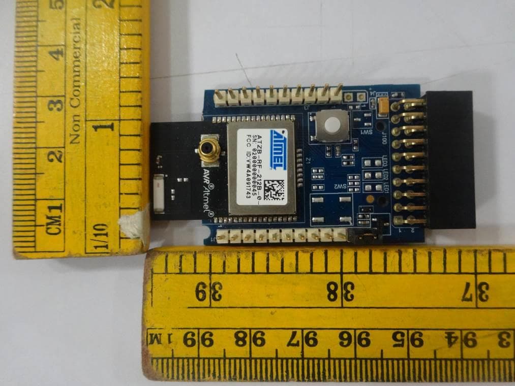
Click to zoom
Application Details
- Equipment Class
- DTS - Digital Transmission System
- Date of Grant
- Jan 06, 2014
- Application Purpose
- Original Equipment
- Date of Application
- Jan 01, 2014
- Equipment Note
- ATZB-RF-212B-0-CN Sub GHz Transciever ZigBit Module
- Frequency Range
- 906.00000000 - 924.00000000
- Company
- Microchip Technology Inc.
- Country
- United States
Documents & Files
Document Text
Text extracted from the exhibit documents filed with the FCC. Open a document above to read the original.
Users Manual
ZIGBIT 900 MHZ WIRELESS MODULES ATZB-RF-212B-0-CN DATASHEET Features Ultra Compact size (30.0 x 20.0 mm) MCU less Tranceiver module with SPI interface High RX sensitivity (-103 dBm) Outperforming link budget (up to +112 dB) Up to +9.0 dBm output power Very low power consumption: 8.7 mA in RX mode (1) 27 mA in TX mode (1) 0.7 μA in sleep mode (2) Internal Clock Output Preassigned Atmel ® MAC address that can be used on end product Capability to use MAC address into the onboard EEPROM IEEE ® 802.15.4 compliant Transceiver 900MHz ISM band Rapid design-in with built-in Chip Antenna RF Test point using MS-147 RF connector Small physical footprint and low profile for optimum fit in very small application boards Mesh networking capability Easy-to-use low cost development kit Single source of support for HW and SW Worldwide license-free operation Note: 1. MCU is in active state with 3V Supply, CPU clock @ 16MHz, RX RPC enabled (for RX current), PHY_TX_PWR=0x0 (for TX current), All digital outputs pulled high. Note: 2. Controller Sleep Mode – SLEEP_MODE_PWR_DOWN Error! Reference source not found. [ZigBit 900 MHz Wireless Modules] 2 Table of Contents 1. Introduction ........................................................................................ 3 1.1 Summary ........................................................................................................... 3 1.2 Applications ....................................................................................................... 3 1.3 Abbreviations and acronyms ............................................................................. 3 1.4 Related documents ........................................................................................... 4 2. ZigBit Module Overview ..................................................................... 6 2.1 Overview ........................................................................................................... 6 3. Specification....................................................................................... 8 3.1 Electrical Characteristics ................................................................................... 8 3.1.1 Absolute Maximum Ratings ................................................................ 8 3.1.2 Power Supply ...................................................................................... 8 3.1.3 RF Characteristics .............................................................................. 9 3.2 Physical/environmental characteristics and outline ......................................... 10 3.3 Pin configuration ............................................................................................. 10 3.4 Antenna Orientation Recommendation ........................................................... 11 3.5 Mounting information ....................................................................................... 11 3.6 Soldering profile .............................................................................................. 16 3.7 Antenna reference designs ............................................................................. 17 4. Section 4 .......................................................................................... 17 4.1.1 General recommendations ................................................................ 17 5. Persistence Memory ........................................................................ 18 6. Ordering information ........................................................................ 18 7. Agency Certifications ....................................................................... 19 7.1 United States (FCC) ........................................................................................ 19 7.2 Canada (IC) .................................................................................................... 19 Appendix A. Revision history ........................................................... 21 Error! Reference source not found. [ZigBit 900 MHz Wireless Modules] 3 1. Introduction 1.1 Summary ATZB-RF-212B-0-CN ZigBit ® is an ultra-compact and low-power 900 MHz IEEE 802.15.4/ZigBee ® OEM module from Atmel ® . Based on the innovative mixed-signal hardware platform from Atmel, this module uses the AT86RF212B [4] 700/800/900 MHz ISM band Transceiver alone on a very compact Module design that provides the customer to integrate the module to any of the recommended Atmel’s Microcontrollers that the application fits. The radio transceiver provides high data rates from 20 kb/s up to 1 Mb/s, frame handling, outstanding receiver sensitivity and high transmit output power enabling a very robust wireless communication. The module is designed for wireless sensing, monitoring, control, data acquisition applications, to name a few. This ZigBit module eliminates the need for costly and time- consuming RF development, and shortens time-to-market for wireless applications. The module has an MS-147 RF connector that can be used as an RF test port. The built-in chip antenna is designed and tuned for the ZigBit design to enable quick integration of the ZigBit into any application. 1.2 Applications The ZigBit module is compatible with robust IEEE 802.15.4/ZigBee stack that supports a self-healing, self-organizing mesh network, while optimizing network traffic and minimizing power consumption. For detailed Software support information, please visit www.atmel.com/wireless The applications include, but are not limited to: Building automation & monitoring o Lighting controls o Wireless smoke- and CO-detectors o Structural integrity monitoring HVAC monitoring & control Inventory management Environmental monitoring Security Water metering Industrial monitoring o Machinery condition and performance monitoring o Monitoring of plant system parameters such as temperature, pressure, flow, tank level, humidity, vibration, etc. Automated mete…
Text truncated - open the document above for the full version.
Block Diagram
Atmel Norway AS Vestre Rosten 79, 7075 Tiller, Norway Tlf:+47 72 88 43 88 Fax +47 72 88 43 99 24-Dec-13 To whomsoever it may concern Product Block diagram This document features the internal block diagram of the product mentioned below. Product name: ZigBit AT86RF212B Product Model: ATZB-RF-212B-0-CN FCC ID: VW4A091743 Product Block diagram: S P I T R X C T R L R E S E T XOSC - 16 MHz crystal C L K M D I G 1 - 4 MS 147 connector C h i p A n t e n n a AT86RF212B Transceiver Balun RFN AVREG 1.8VDVREG 1.8V RFP Atmel Norway AS Vestre Rosten 79, 7075 Tiller, Norway Tlf:+47 72 88 43 88 Fax +47 72 88 43 99 Internal Block diagram of AT86RF212B RF Transceiver IC, showing Internal Voltage Regulator – AVREG, DVREG Sincerely, Saravanakumar Marudhachalam Manager, Tools HW Development, Atmel Norway AS
Cover Letter(s)
Atmel Norway AS Vestre Rosten 79, 7075 Tiller, Norway Tlf:+47 72 88 43 88 Fax +47 72 88 43 99 Applicant/Grantee Atmel Norway AS FCC ID: VW4A091743 Section 15.212 Modular Transmitters Request for Single Modular Approval Request for Limited Single Modular approval SI. No Requirements EUT Conditions Comply (Y/N) 01 The radio elements of the modular transmitter must have their own Shielding. The physical crystal and tuning capacitors may be located external to the shielded radio elements The Module has its own shielding. Shielding can be employed on the board structure. Y 02 The modular transmitter must have buffered modulation/data inputs (if such inputs are provided) to ensure that the module will comply with Part 15 requirements under conditions of excessive data rates or over-modulation All Modulation and data input(s) are buffered. Refer block diagram and schematic diagram. Y 03 The modular transmitter must have its Own power supply regulation. The AT86RF212B IC has internal power supply regulator of 1.8V, that is used to power the Radio core Y 04 The modular transmitter must comply with the antenna and transmission system requirements of Sections 15.203, 15.204(b) and 15.204(c). The antenna must either be permanently attached or employ a “unique” antenna coupler (at all connections between the module and The antenna, including the cable). The “professional installation” provision of Section 15.203 is not applicable to modules but can apply to limited Modular approvals under paragraph (b) of this section. An RF measurement port is provided with a unique connector for probing purpose. Please refer attached query response from FCC in appendix. The Antenna for the module is Built-in Chip Antenna Y 05 The modular transmitter must be tested in a stand-alone configuration, i.e., the module must not be inside another device during testing for compliance With Part 15 requirements. Unless the transmitter module will be battery powered, it must comply with the AC line conducted requirements found in Section 15.207. AC or DC power lines and data input/output lines connected to the module must not contain ferrites, unless they will be marketed with the Y Atmel Norway AS Vestre Rosten 79, 7075 Tiller, Norway Tlf:+47 72 88 43 88 Fax +47 72 88 43 99 Module (see Section 15.27(a)). The length of these lines shall be the length typical of actual use or, if that length is unknown, at least 10 centimeters to insure that there is no coupling between the case of the module and supporting Equipment. Any accessories, peripherals, or support equipment connected to the module during testing shall be Unmodified and commercially available (see Section 15.31(i)). 06 The modular transmitter must be equipped with either a permanently affixed label or must be capable of electronically displaying its FCC Identification number. (A) If using a permanently affixed label, the modular transmitter must be labeled with its own FCC identification number, and, if the FCC identification number is not visible when the module is installed inside another device, then the outside of the device into which the module is Installed must also display a label referring to The enclosed module. This exterior label can use wording such as the following: “Contains Transmitter Module FCC ID: XYZMODEL1” or “Contains FCC ID: XYZMODEL1.” Any similar wording That expresses the same meaning may be used. The Grantee may either provide such a label, an example of which must be included in the application for equipment authorization, or, must provide adequate Instructions along with the module which explain This requirement. In the latter case, a copy of these instructions must be included in the Application for equipment authorization. (B) If the modular transmitter uses an electronic display of the FCC identification number, the information must be readily accessible and visible on the modular transmitter or on the Device in which it is installed. If the module is installed inside another device, then the outside of the device into which the module Refer Zigbit RF212B User Manual document. Y Atmel Norway AS Vestre Rosten 79, 7075 Tiller, Norway Tlf:+47 72 88 43 88 Fax +47 72 88 43 99 is installed must display a label referring to the enclosed Module. This exterior label can use wording such as the following: “Contains FCC certified transmitter module(s).” Any similar wording that expresses the same Meaning may be used. The user manual must include instructions on how to access the Electronic display. A copy of these instructions Must be included in the application for equipment authorization. 07 The modular transmitter must comply with any specific rules or operating requirements that ordinarily apply to a complete transmitter and the manufacturer must provide adequate instructions along with the module to explain any such Requirements. A copy of these Instructions must be included in the application for equipment authorization. . Refer Zigbit RF212B User Manual document. Y 08 The modular transmitter must comply with any applicable RF exposure requirements in its final configuration Y A limited modular approval may be granted for single or split modular transmitters that do not comply with all of the above requirements, e.g., shielding, minimum signaling amplitude, buffered modulation/data inputs, or power supply regulation, if the manufacturer can demonstrate by alternative means in the application for equipment authorization that the modular transmitter meets all the applicable Part 15 requirements under the operating conditions in which the transmitter will be used. Limited modular approval also may be granted in those instances where compliance with RF exposure rules is demonstrated only for particular product configurations. The applicant for certification must state how control of the end product into which the module will be installed will be maintained such that full compliance of the end product is always ensured Sincerely, Saravanakumar Ma…
Text truncated - open the document above for the full version.
External Photos
www.tuv.com Appendix 2 Prüfbericht - Nr.: Test Report No. 19660041 001 Seite 1 von 2 Page 1 of 2 Module Top View Module Bottom View www.tuv.com Appendix 2 Prüfbericht - Nr.: Test Report No. 19660041 001 Seite 2 von 2 Page 2 of 2 Module Dimensional View
ID Label/Location Info
www.tuv.com Appendix 4 Prüfbericht - Nr.: Test Report No. 19660041 001 Seite 1 von 1 Page 1 of 1 Label Diagram Label Location
Internal Photos
www.tuv.com Appendix 3 Prüfbericht - Nr.: Test Report No. 19660041 001 Seite 1 von 1 Page 1 of 1 Module- Shielding Removed
Operational Description
Atmel Norway AS Vestre Rosten 79, 7075 Tiller, Norway Tlf:+47 72 88 43 88 Fax +47 72 88 43 99 24-Dec-13 Theory of Operation/Technical Description – FCC ID: VW4A091743 - RF circuit function: The IEEE 802.15.4 compliant AT86RF212B transceiver generates a modulated carrier wave at 906- 924MHz with 10 IEEE 802.15.4 channels. This transceiver circuit is used by system applications as a physical layer for ZigBee applications. - RF signal flow: The Transceiver IC outputs a differential RF signal- RFP & RFN which is converted to single ended by the balun and then passes through the RF path till the antenna and gets radiated or vice versa during reception - Description of Antenna system: RF signal from/to the front end goes to MS147 Antenna connector and then through tuning elements to the chip antenna. Tuning elements are present to ensure compliance. - Compliance with 15.203 antenna requirements: FCC 15.203 requirements for this design are tested and verified during FCC compliance testing. - Description of all modulation schemes used in the product: Module uses BPSK and O-QPSK with half-sine pulse shaping. Saravanakumar Marudhachalam Manager, Tools HW Development
Operational Description
www.tuv.com Appendix 6 Prüfbericht - Nr.: Test Report No. 19660041 001 Seite 1 von 1 Page 1 of 1 Specifications of EUT Operating Frequency 902 - 928 MHz No. of channel 10 Channel Spacing 2 MHz Modulation DSSS [BPSK] Transmitted Power 10.52dBm Data Rate 250 kbps Antenna Type Ceramic Chip Antenna Number of antenna One Antenna Gain 0dBi Supply Voltage 1.8VDC – 3.6VDC Dimensions 20mm x 30mm Environmental -40 degrees to +85 degrees C
Operational Description
Atmel Norway AS Vestre Rosten 79, 7075 Tiller, Norway Tlf:+47 72 88 43 88 Fax +47 72 88 43 99 24-Dec-13 To whomsoever it may concern Product Application This document explains the nature of intended application of the product mentioned below. Product name: ZigBit RF212B Product Model: ATZB-RF-212B-0-CN FCC ID: VW4A091743 Product Application: The ZigBit RF212B is a Zigbit module of the Atmel AT86RF212B radio transceiver. The radio transceiver supports the worldwide accessible 900MHz ISM band. The system is designed standard-based applications such as ZigBee/IEEE 802.15.4, ZigBee RF4CE, and 6LoWPAN, as well as high data rate ISM applications. Sincerely, Saravanakumar Marudhachalam Manager, Tools HW Development, Atmel Norway AS
Operational Description
915 MHz AntennaP/N 0915AT43A0026 Detail Specification: 07/26/2010 Page 1 of 3 Recommended Application ISM General Specifications Part Number0915AT43A0026Operating Temperature-40 to +85°C Frequency Range902 - 928 Storage Temperature+5~+35°C, Peak Gain-1.0 dBi typ. (XZ-total) RangeHumidity 45~75%RH Average Gain-4.0 dBi typ. (XZ-total)Reel Quanity1,000 Return Loss8.5 dB min. Impedance50 Ω Input Power2W max.No.FunctionTerminal Configuration 1 2 Mechanical Dimensions Inmm L±± W±± T a±± Mounting Considerations Mount these devices with brown mark facing up. Units: mm * Line width should be designed to provide 50 Ω impedance matching characteristics. With Matching Circuit **matching circuit and component values will depend on PCB layout, thickness, material, etc. Johanson Technology, Inc. reserves the right to make design changes without notice. All sales are subject to Johanson Technology, Inc. terms and conditions. www.johansontechnology.com 4001 Calle Tecate • Camarillo, CA 93012 • TEL 805.389.1166 FAX 805.389.1821 2010 Johanson Technology, Inc. All Rights Reserved "High Frequency Ceramic Solutions" 0.0080.2767.000.20 0.80 0.0200.012 +0.1/-0.2 0.079 0.031 2.00 +.004/-.008 0.008 Feeding Point NC 0.20 0.500.30 GND Plane GND Plane 1 2 L W a T JTI P/N for Matching Circuit:** Inductor (4.7nH):L-07C4N7SV6T Inductor (10nH): L-07C10NJV6T Cap (0.5pF): 500R07S0R5BV4T 2.0 5.5 8.0 1.0 5.0 7.0 2.5 0.5 0.5 pF 10 nH 4.7 nH Matching circuits** * 915 MHz AntennaP/N 0915AT43A0026 Detail Specification: 07/26/2010 Page 2 of 3 Recommended Application ISM Mounting Considerations Test Board Johanson Technology, Inc. reserves the right to make design changes without notice. All sales are subject to Johanson Technology, Inc. terms and conditions. www.johansontechnology.com 4001 Calle Tecate • Camarillo, CA 93012 • TEL 805.389.1166 FAX 805.389.1821 2010 Johanson Technology, Inc. All Rights Reserved "High Frequency Ceramic Solutions" ) ) ) ) ) ) ) ) ) Antenna Ground 20mm 40mm9.5mm 50Ω Feed Line Return Loss (with matching) Antenna No Ground Ground 20mm 19mm 40mm 9.5mm 50Ω Feed Line 0.60.70.80.91.01.11.20.51.3 -40 -35 -30 -25 -20 -15 -10 -5 -45 0 freq, GHz dB(S(1,1)) m1 m2 m3 m1 freq= dB(S(1,1))=-11.21 7 902.0MHz m2 freq= dB(S(1,1))=-11.80 7 928.0MHz m3 freq= dB(S(1,1))=-43.25 7 915.0MHz 915 MHz AntennaP/N 0915AT43A0026 Detail Specification: 07/26/2010 Page 3 or 3 Recommended Application ISM Johanson Technology, Inc. reserves the right to make design changes without notice. All sales are subject to Johanson Technology, Inc. terms and conditions. www.johansontechnology.com 4001 Calle Tecate • Camarillo, CA 93012 • TEL 805.389.1166 FAX 805.389.1821 2010 Johanson Technology, Inc. All Rights Reserved "High Frequency Ceramic Solutions" ) ) ) ) ) ) ) ) ) Typical Radiation Patterns ) ) ) ) ) ) ) ) ) XY-V/XY-H 180° 270° 0° 90° X Z Y XY-cut scanning direction XY cut @915MHz Vertical Horizontal XZ-V/XZ-H YZ-V/YZ-H 180° 270° 0° 90° X Z Y XZ-cut scanning direction 180° 270° 0° 90° X Z Y YZ-cut scanning direction YZ cut @915MHz Vertical Horizontal XZ cut @915MHz Vertical Horizontal
Parts List/Tune Up Info
Component list Bill of Materials Print For Variant [RFmodule_212B_Variant-NA] of Project [RFonly_212B.PrjPCB] (No PCB Document Selected) Source Data From:RFonly_212B.PrjPCB Project:RFonly_212B.PrjPCB Variant:RFmodule_212B_Variant-NA Report Date:11/18/201312:04:58 PM Print Date:11/18/201312:04:57 PM #DesignatorQuantityValueManufacturerMPNDescription 1A110915AT43A0026Johanson Technology0915AT43A0026Sub 1GHz Chip Antenna 2B110896FB15A0100Johanson Technology0896FB15A0100868/900MHz FilterBalun, SMD 1.25x2.0mm (de26948) 3C1, C2, C6, C741uFAVX0603YD105KAT2ACAP CER 1UF 16V 10% X5R 0603 4C312.2 pFKemetCBR02C229C9GACCAP CER 2.2PF 6.3V NP0 0201 5C5, C8210 pFMurataGRM0335C1E100JA01DCeramic capacitor, SMD 0201, C0G, 25V, +-0.25pF 6C91100nKemetC0201C104K9PACTUCAP CER 0.1UF 6.3V 10% X5R 0201 7C10168pFPanasonicECJ-0EC1H680JCAP CER 68PF 50V 5% NP0 0402 8C1115.6pFJohanson Technology250R05L5R6CV4TCAP CER 5.6PF 25V NP0 0201 9J11MS147HIROSECL358-150-5-01Interface RF Connector with Switch, 10L31BLM15BB221SN1MurataBLM15BB221SN1SMD RF inductor 0402. Z=220Ohm (@100MHz), Max R(dc)=0.80Ohm, Max current=200mA 11L411.8nHJohanson TechnologyL-05B1N8SV6Tceramic chip inductor, 1.8nH,0201 12LABEL11Label PCBAACT Logimark AS505462PCBA identification label PP Top White Gloss 13PCB11ZigBit Sub-GHz RF-only board PCB ZigBit Sub-GHz RF-only board PCB 14Q1116.0MHzEpson ToyocomTSX-3225 16.0000MF09Z-AC316MHz uXtal, 3.2 x 2.5 mm SMD, CL=9pF, 15PPM, ESR=80ohm(Max. 15R11680RYAGEO CORPRC0201JR-07680RLRES 680 OHM 1/20W 5% 0201 SMD 16R5, R6210 kROHMMCR006YZPJ103+Thick film resistor, SMD 0201, 1/20W, 5% 17U11AT86RF212B-ZUATMELAT86RF212B-ZULow Power 700/800/900 MHz Transceiver for IEEE 802.15.4, ZigBee, 6LoWPAN, and ISM Applications (de34572) 18U21AT24MAC602-STUM-TATMELAT24MAC602-STUM-T2kbit Serial (TWI) EEPROM, AT24C02B, 1.8-5V 19Z11ATZB-RF-4-0-C-915ATMELATZB-RF-4-0-C-915ZigBit RF-only SUB_GHz-915 20Z21EMI ShieldDUFU INDUSTRIES SDN BHDEMI Shield ZigBit RF212B 25 Notes Approved Altium Limited Confidential 11/18/2013Page 1
RF Exposure Info
www.tuv.com Appendix 10 Prüfbericht - Nr.: Test Report No. 19660041 001 Seite 1 von 2 Page 1 of 2 RF Exposure Report RF Exposure Measurement The limit for Maximum Permissible Exposure (MPE) specified in FCC 1.1310 is followed. The gain of the antennas used in the product is extracted from the Antenna data sheets provided and also the maximum total power input to the antenna is measured. Through the Friis transmission formula and the maximum gain of the antenna, we can calculate the distance, away from the product, where the limit of MPE is reached. Although the Friis Transmission formula is far field assumption, the calculated result of that is an over- prediction for near field power density. It is taken as worst case to specify the safety range. RF Exposure Limit According to FCC 1.1310: The criteria listed in the following table shall be used to evaluate the environmental impact of the human exposure to radio-frequency (RF) radiation as specified in 1.1307 (b) Limits for Maximum Permissible Exposure (MPE) Frequency Range (MHz) Electric Field Strength (V/m) Magnetic Field Strength (A/m) Power Density (mW/cm²) Limits for Occupational / controlled Exposures 300 - 1500 -- -- F/300 1500 – 100000 -- -- 5.0 Limits for General population / Uncontrolled Exposure 300 - 1500 -- -- F/1500 1500 – 100000 -- -- 1.0 F= Frequency in MHz www.tuv.com Appendix 10 Prüfbericht - Nr.: Test Report No. 19660041 001 Seite 2 von 2 Page 2 of 2 Friss Formula Friss Transmission Formula: Pd = (Pout * G) / (4*pi*r²) Where Pd = power density in mW/cm² Pout = output power to antenna in mW G = gain of antenna in linear scale Pi = 3.1416 R = Distance between observation point and the center of radiator in cm If we know the maximum gain of the antenna and the total output power to the antenna, through calculation, we will know MPE value at distance 20cm. EUT Operation condition EUT was enabled to transmit and receive at lowest, middle and highest channels. Classification The antenna of this product, under normal use condition, is at least 20cm away from the body of the user. Warning statement to the user for keeping at least 20cm or more separation distance from the antenna should be included in the User manual. So, this device is classified as Mobile device. Test Results Highest measured power at 906 MHz i.e. 10.52dBm Gain (G) = 0dBi=1(Linear) Channel Frequency (MHz) Output Power to Antenna (mW) Power Density (mW/cm²) Limit (mW/cm²) 906 11.27197 0.002242 1.000
Schematics
1 1 2 2 3 3 4 4 5 5 6 6 7 7 8 8 DD CC BB AA A08-1565 RFonly_212B.SchDoc 1111/4/20136:13:21 PM ZigBit 900MHz RF-Only ATMEL Chennai RMZ Millenia 2 PERUNGUDI,CHENNAI INDIA PAGE:of TITLE: Document number:Revision:3 Date: OJS MSK * GND GND RESET_N SLP_TR CLKM DIG3 DIG4 IRQ nSEL MOSI SCLK MISO DIG2 DIG1 GND GND i PCB Rule i PCB Rule RESET_N IRQ GND GND MAC_SCL MAC_SDA AN_VCC_3V3 VCC_3V3 VCC_3V3CLKM VCC_3V3 DIG4 2 AVSS 3 RFP 4 RFN 5 AVSS 6 DVSS 7 /RST 8 D I G 1 9 D I G 2 1 0 S L P _ T R 1 1 D V S S 1 2 D V D D 1 3 D V D D 1 4 D E V D D 1 5 D V S S 1 6 CLKM 17 DVSS 18 SCLK 19 MISO 20 DVSS 21 MOSI 22 /SEL 23 IRQ 24 X T A L 2 2 5 X T A L 1 2 6 A V S S 2 7 E V D D 2 8 A V D D 2 9 A V S S 3 0 A V S S 3 1 A V S S 3 2 DIG3 1 P A D 3 3 AT86RF212B-ZU U1 GND GND 50Ohm 1 G N D 2 Bal 3 Bal 4 G N D 5 G N D 6 0896FB15A0100B1 GND SLP_TR MAC_SCL MAC_SDA DIG2 MISO MOSI SCLK nSEL GND 0R R2 0R R3 GND 2 SDA 3 SCL 1 WP 5 VCC 4 AT24MAC602-STUM-T U2 VCC_3V3 GND ZigBit Sub-GHz RF-only board PCB PCB1 AN_VCC_3V3VCC_3V3 BLM15BB221SN1 L3 1uF C6 1uF C7 1uF C1 1uF C2 2.2 pF C3 10 pF C5 10 pF C8 100nC9 1 0 k R 5 1 0 k R 6 680R R1 Product number/revision Serial number Label PCBALABEL1 RF_N RF_P FEED POINT 1 NC 2 0915AT43A0026 A1 RF_IN 1 RF_OUT 2 G N D 3 G N D 4 MS147J1 3.3nH L2 GND GND GND GND GNDGND GNDGNDGND GNDGND 68pF C10 GND 1 nRST 5 VDD 3 GND 2 DIG2 34 SLP_TR 35 SCL 36 SDA 37 MISO 8 MOSI 7 nSEL 6 FEM_SEL 38 GND 41 VDD 4 IRQ 40 GND 42 CLKM 39 SCLK 9 DIG1 10 FEM_CSD 11 DIG4 33 DIG3 32 ATZB-RF-4-0-C-915 Z1 DIG1 DIG3 DIG4 1 3 2 4 16.0MHz Q1 1234 EMI Shield Z2 B a 1.8nHL4 5 . 6 p F C 1 1 tune the values for Antenna matching Place de-coupling closer to TRX Place de-coupling closer to TRX Place xtal circuit closer to TRX . Isolate from digital signals. BoM Varients for Antenna: Japanese/North American Band 0915AT43A0026 European Band 0868AT43A0020 Chinese Band 0783AT43A0008 BoM Varients: Japanese/North American Band DNI-R2, DNI-R3 European Band Mount-R2, DNI-R3 Chinese Band Mount-R2, Mount-R3 Layout: Maintain two ground planes and two power planes BoM varients for Balun: Jap/NA Band 0896FB15A0100 European Band 0896FB15A0100 Chinese Band 0783FB15A0100 PIA101PIA102 COA1 PIB101 PIB102 PIB103 PIB104 PIB105PIB106 COB1 PIC101 PIC102 COC1 PIC201 PIC202 COC2 PIC301PIC302 COC3 PIC501PIC502 COC5 PIC601PIC602 COC6 PIC701PIC702 COC7 PIC801PIC802 COC8 PIC901PIC902 COC9 PIC1001PIC1002 COC10 PIC1101 PIC1102 COC11 PIJ101PIJ102 PIJ103 PIJ104 COJ1 PIL201 PIL202 COL2 PIL301PIL302 COL3 PIL401PIL402 COL4 COLABEL1 COPCB1 PIQ101 PIQ102 PIQ103 PIQ104 COQ1 PIR101PIR102 COR1 PIR201PIR202 COR2 PIR301PIR302 COR3 PIR501 PIR502 COR5 PIR601 PIR602 COR6 PIU101 PIU102 PIU103 PIU104 PIU105 PIU106 PIU107 PIU108 PIU109PIU1010PIU1011PIU1012PIU1013PIU1014PIU1015PIU1016 PIU1017 PIU1018 PIU1019 PIU1020 PIU1021 PIU1022 PIU1023 PIU1024 PIU1025PIU1026PIU1027PIU1028PIU1029PIU1030PIU1031PIU1032PIU1033 COU1 PIU201 PIU202 PIU203 PIU204 PIU205 COU2 PIZ101 PIZ102 PIZ103 PIZ104 PIZ105 PIZ106 PIZ107 PIZ108 PIZ109 PIZ1010 PIZ1011PIZ1032 PIZ1033 PIZ1034 PIZ1035 PIZ1036 PIZ1037 PIZ1038 PIZ1039 PIZ1040 PIZ1041 PIZ1042 COZ1 PIZ201PIZ202PIZ203PIZ204 COZ2 PIC701 PIL301 PIU1028 PIC301PIR101 PIZ1039 PIU109 PIZ1010 PIU1010 PIZ1034 PIU101 PIZ1032 PIU102 PIZ1033 PIB102 PIB105PIB106 PIC101 PIC202 PIC302 PIC501 PIC602 PIC702 PIC801 PIC901 PIC1102 PIJ103 PIJ104 PIL202 PIQ102 PIQ104 PIU103 PIU106 PIU107 PIU1012PIU1016 PIU1018 PIU1021 PIU1027PIU1030PIU1031PIU1032PIU1033 PIU202PIU205 PIZ101 PIZ102PIZ1041 PIZ1042 PIZ201PIZ202PIZ203PIZ204 PIU1024 PIZ1040 PIR601 PIU201 PIZ1036 PIR501 PIU203 PIZ1037 PIU1020 PIZ108 PIU1022 PIZ107 PIZ1038 PIZ1011 PIR302PIR202PIR301 PIR102PIU1017 PIJ102 PIL201 PIL402PIC1002PIJ101 PIC802 PIQ101 PIU1026 PIC601 PIU1029 PIC502 PIQ103 PIU1025 PIC102 PIU1013PIU1014 PIB101PIC1001PIA102PIR201PIA101 PIC1101 PIL401 PIU1023 PIZ106 PIU108 PIZ105 PIB103PIU105 NLRF0N PIB104 PIU104 NLRF0P PIU1019 PIZ109 PIU1011 PIZ1035 PIC201 PIC902 PIL302 PIR502PIR602 PIU1015 PIU204 PIZ103 PIZ104
Schematics
PAA102 PAA101 COA1 PAB104 PAB105 PAB106 PAB103 PAB102 PAB101 COB1 PAC101 PAC102 COC1 PAC201 PAC202 COC2 PAC302 PAC301 COC3 PAC401 PAC402 COC4 PAC502PAC501 COC5 PAC601 PAC602 COC6 PAC701PAC702 COC7 PAC802PAC801 COC8 PAC902 PAC901 COC9 PAC1002PAC1001 COC10 PAJ103 PAJ104 PAJ101 PAJ102 COJ1 PAL102PAL101 COL1 PAL202PAL201 COL2 PAL301 PAL302 COL3 COLABEL1 PAQ101 PAQ102PAQ103 PAQ104 COQ1 PAR101 PAR102 COR1 PAR201PAR202 COR2 PAR301 PAR302 COR3 PAR501 PAR502 COR5 PAR601 PAR602 COR6 PAU1033 PAU1032 PAU1031 PAU1030 PAU1029 PAU1028 PAU1027 PAU1026 PAU1025 PAU1024PAU1023PAU1022PAU1021PAU1020PAU1019PAU1018PAU1017 PAU1016 PAU1015 PAU1014 PAU1013 PAU1012 PAU1011 PAU1010 PAU101PAU102PAU103PAU104PAU105PAU106PAU107PAU108 PAU109 COU1 PAU201 PAU202 PAU203PAU204 PAU205 COU2 PAZ101 PAZ1042PAZ1041PAZ1040PAZ1039PAZ1038PAZ1037PAZ1036PAZ1035PAZ1034PAZ1033PAZ1032PAZ1031PAZ1030PAZ1029PAZ1028PAZ1027PAZ1026 PAZ1025 PAZ1024 PAZ1023 PAZ1022 PAZ1021 PAZ1020 PAZ1019 PAZ1018 PAZ1017PAZ1016PAZ1015PAZ1014PAZ1013PAZ1012PAZ1011PAZ1010PAZ109PAZ108PAZ107PAZ106PAZ105PAZ104PAZ103PAZ102 COZ1 PAZ201PAZ204 PAZ203PAZ202 COZ2 PAC701 PAL301 PAU1028 PAC301PAR101 PAZ1039 PAU109 PAZ1010 PAU1010 PAZ1034 PAU101 PAZ1032 PAU102 PAZ1033 PAB102PAB105 PAB106 PAC101 PAC202 PAC302 PAC501 PAC602 PAC702 PAC801 PAC901 PAJ103 PAJ104 PAL102 PAL202 PAQ102 PAQ104 PAU103PAU106PAU107 PAU1012 PAU1016 PAU1018PAU1021 PAU1027 PAU1030 PAU1031 PAU1032 PAU1033 PAU202 PAU205 PAZ101PAZ102 PAZ1041PAZ1042 PAZ201 PAZ202PAZ203 PAZ204 PAU1024 PAZ1040 PAR601 PAU201 PAZ1036 PAR501 PAU203 PAZ1037 PAU1020 PAZ108 PAU1022 PAZ107 PAA101 PAC402 PAL101 PAA102 PAR201 PAB101 PAC1001 PAC102 PAU1013 PAU1014 PAC401 PAJ102 PAL201 PAC502 PAQ103 PAU1025 PAC601 PAU1029 PAC802 PAQ101 PAU1026 PAC1002PAJ101 PAR102 PAU1017 PAR202 PAR301 PAU1023 PAZ106 PAU108 PAZ105 PAB103 PAU105 PAB104 PAU104 PAU1019 PAZ109 PAU1011 PAZ1035 PAC201 PAC902 PAL302 PAR502 PAR602 PAU1015 PAU204 PAZ103PAZ104 PAA102 PAA101 COA1 PAB104 PAB105 PAB106 PAB103 PAB102 PAB101 COB1 PAC101 PAC102 COC1 PAC201 PAC202 COC2 PAC302 PAC301 COC3 PAC401 PAC402 COC4 PAC502PAC501 COC5 PAC601 PAC602 COC6 PAC701PAC702 COC7 PAC802PAC801 COC8 PAC902 PAC901 COC9 PAC1002PAC1001 COC10 PAJ103 PAJ104 PAJ101 PAJ102 COJ1 PAL102PAL101 COL1 PAL202PAL201 COL2 PAL301 PAL302 COL3 COLABEL1 PAQ101 PAQ102PAQ103 PAQ104 COQ1 PAR101 PAR102 COR1 PAR201PAR202 COR2 PAR301 PAR302 COR3 PAR501 PAR502 COR5 PAR601 PAR602 COR6 PAU1033 PAU1032 PAU1031 PAU1030 PAU1029 PAU1028 PAU1027 PAU1026 PAU1025 PAU1024PAU1023PAU1022PAU1021PAU1020PAU1019PAU1018PAU1017 PAU1016 PAU1015 PAU1014 PAU1013 PAU1012 PAU1011 PAU1010 PAU101PAU102PAU103PAU104PAU105PAU106PAU107PAU108 PAU109 COU1 PAU201 PAU202 PAU203PAU204 PAU205 COU2 PAZ101 PAZ1042PAZ1041PAZ1040PAZ1039PAZ1038PAZ1037PAZ1036PAZ1035PAZ1034PAZ1033PAZ1032PAZ1031PAZ1030PAZ1029PAZ1028PAZ1027PAZ1026 PAZ1025 PAZ1024 PAZ1023 PAZ1022 PAZ…
Text truncated - open the document above for the full version.
Contact Information
Applicant
Steve Caldwell(Vice President, Wireless Solutions Group)
Test Firm
TUV Rheinland (India) Pvt. Ltd.,B GURUPRASAD
Technical Specifications
| # | Rule Parts | Frequency Range | Power Output |
|---|---|---|---|
| 1 | 15C | 906 MHz - 924 MHz | 11.27 mW |
Other Applications from Microchip Technology Inc.
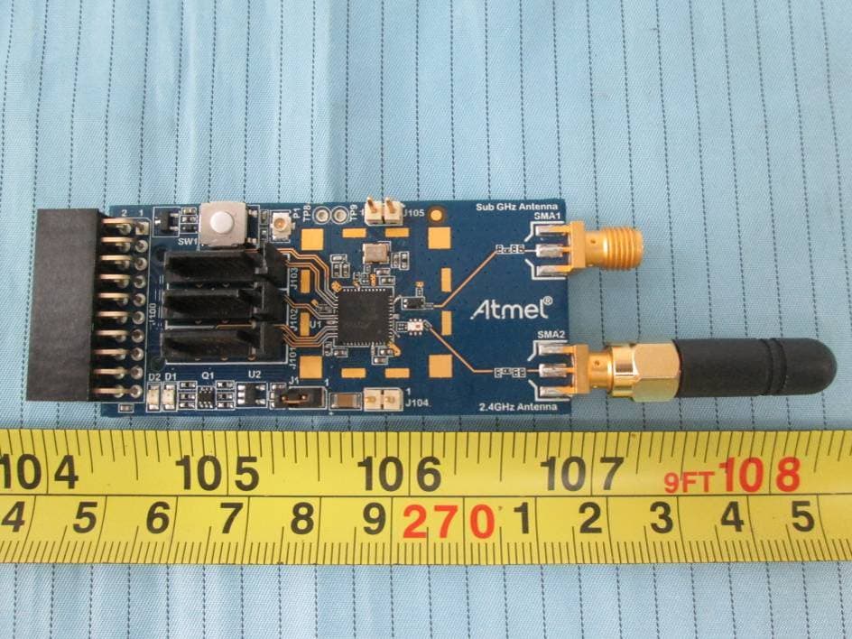
VW4A091980
Dec 22, 2015ATREB215-XPRO
Equipment Class
DXX - Part 15 Low Power Communication Device TransmitterVW4A092412
Mar 27, 2015ATSAMR21ZLL-EK
Equipment Class
DTS - Digital Transmission System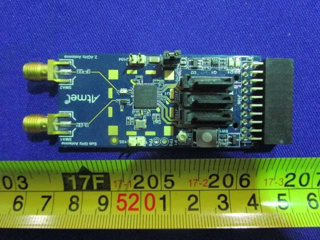
VW4A091982
Mar 21, 2015ATREB215-XPRO
Equipment Class
DTS - Digital Transmission System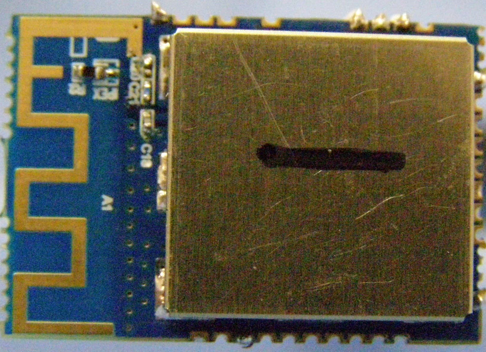
VW4ATWILC1000
Dec 03, 2014Wireless Module
Equipment Class
DTS - Digital Transmission System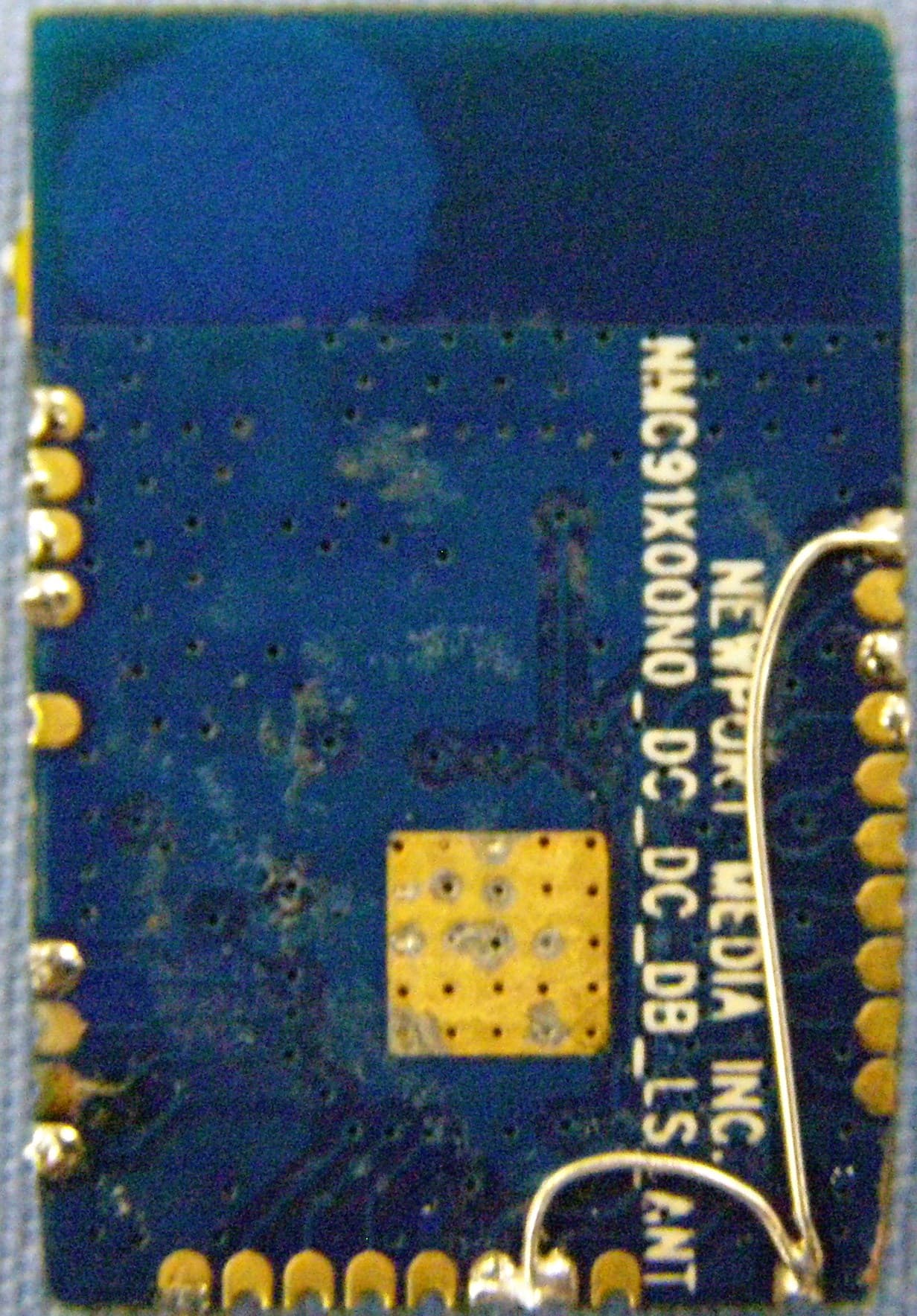
VW4ATWINC1500
Nov 17, 2014Wireless Module
Equipment Class
DTS - Digital Transmission System