VZFSWP23MA2802.11b/g/n Wi-Fi Module with Access Point Function
Suga Electronics Limited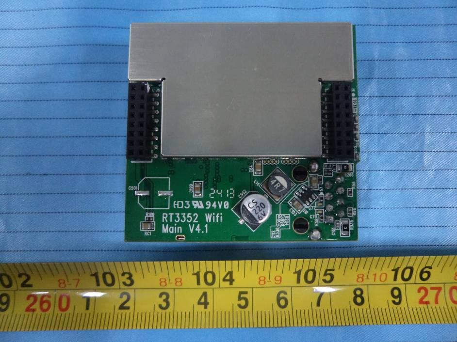
Click to zoom
Application Details
- Equipment Class
- DTS - Digital Transmission System
- Date of Grant
- Jul 17, 2013
- Application Purpose
- Original Equipment
- Date of Application
- Jul 17, 2013
- Equipment Note
- 802.11b/g/n Wi-Fi Module with Access Point Function
- Frequency Range
- 2422.00000000 - 2452.00000000
- Company
- Suga Electronics Limited
- Country
- Hong Kong
Documents & Files
Document Text
Text extracted from the exhibit documents filed with the FCC. Open a document above to read the original.
Users Manual
Suga Electronics Limited © Suga Electronics Ltd. All Rights Reserved. Information in this document is subject to change without prior notice P. 1 802.11b/g/n (2T2R) WLAN AP/Router Module User Manual Model: SWP23MA-2 Version: 1.0 18 Jul 2013 Contents 1.1 FCC Caution.................................................................. 2 1.2 FCC Radiation Exposure Statement................................. ..... 2 1.3 IC Warning................................................................ ..... 2 2.0 Hardware Installation............................................................ 3 2.1 Hardware Installation Guide ........................................ 3 3.0 Software Installation............................................................. 4 3.1 Booting up................................................................ 3 3.2 Operation Mode Configuration...................................... 5 3.3 Local Area Network (LAN) Settings............................... 6 3.4 Basic Wireless Settings................................................ 7 3.5 Advanced Wireless Settings.......................................... 8 3.6 Wireless Security/Encryption Settings............................. 9 3.7 Station List.............................................................. 10 4.0 Device Labelling ............................................................. 11 5.0 Disclaimer...................................................................... 11 Suga Electronics Limited © Suga Electronics Ltd. All Rights Reserved. Information in this document is subject to change without prior notice P. 2 1.1 FCC Caution: Any Changes or modifications not expressly approved by the party responsible for compliance could void the user's authority to operate the equipment. This device complies with part 15 of the FCC Rules. Operation is subject to the following two conditions: (1) This device may not cause harmful interference, and (2) this device must accept any interference received, including interference that may cause undesired operation. IMPORTANT NOTE: 1.2 FCC Radiation Exposure Statement: This equipment complies with FCC radiation exposure limits set forth for an uncontrolled environment .This equipment should be installed and operated with minimum distance 20cm between the radiator & your body. This transmitter must not be co-located or operating in conjunction with any other antenna or transmitter. 1.3 IC WARNING: RSS(Category I Equipment): This device complies with Industry Canada licence-exempt RSS standard(s). Operation is subject to the following two conditions: (1) this device may not cause interference, and (2) this device must accept any interference, including interference that may cause undesired operation of the device. Le présent appareil est conforme aux CNR d'Industrie Canada applicables aux appareils radio exempts de licence. L'exploitation est autorisée aux deux conditions suivantes : (1) l'appareil nedoit pas produire de brouillage, et (2) l'utilisateur de l'appareil doit accepter tout brouillage radioélectrique subi, même si le brouillage est susceptible d'en compromettre le fonctionnement. Under Industry Canada regulations, this radio transmitter may only operate using an antenna of a type and maximum (or lesser) gain approved for the transmitter by Industry Canada. To reduce potential radio interference to other users, the antenna type and its gain should be so chosen that the equivalent isotropically radiated power (e.i.r.p.) is not more than that necessary for successful communication. Conformément à la réglementation d'Industrie Canada, le présent émetteur radio peut fonctionner avec une antenne d'un type et d'un gain maximal (ou inférieur) approuvé pour l'émetteur par Industrie Canada. Dans le but de réduire les risques de brouillage radioélectrique à l'intention des autres utilisateurs, il faut choisir le type d'antenne et son gain de sorte que la puissance isotrope rayonnée équivalente (p.i.r.e.) ne dépasse pas l'intensité nécessaire à l'établissement d'une communication satisfaisante. Suga Electronics Limited © Suga Electronics Ltd. All Rights Reserved. Information in this document is subject to change without prior notice P. 3 Suga Electronics Limited © Suga Electronics Ltd. All Rights Reserved. Information in this document is subject to change without prior notice P. 4 2.2 The SWP23MA-2 WLAN module will be installed into the embedded system user various operation systems(OS) such as Windows 2000/XP/CE or Linux.In this OEM manual,we will use Window XP as an example to show you how to install the driver on the OS. The SWP23MA-2 setup Wizard will guide you through the installation procedure.This Wizard will also guide you installing the utility and drivers. Note :The comments and conditions for other OS platform may be different from this chapter. 3.0 Software Installation 3.1 Booting up Connect the power adapter to two 2x 8pin-2.0mm pitch connectors to power up the module, Connect the Ethernet port to the PC, then enter http://10.10.10.254 into Internet Explorer to open the AP/router home page. As below: Suga Electronics Limited © Suga Electronics Ltd. All Rights Reserved. Information in this document is subject to change without prior notice P. 5 3.2 Operation Mode Configuration Select “Operation Mode” to configure the operation mode to fit you environment, in this menu, there are four options, please follow the description to choose the option you needed. If you want the module to act as an AP and Client, you should select “AP Client” mode and “enable” then click “Apply”. Suga Electronics Limited © Suga Electronics Ltd. All Rights Reserved. Information in this document is subject to change without prior notice P. 6 3.3 Local Area Network(LAN) Settings Select “LAN” option to set your home page IP, subnet mask, default gateway etc. the default IP is 10.10.10.254. Suga Electronics Limited © Suga Electronics Ltd. All Rights Reserved. Information in this document is subject to change wit…
Text truncated - open the document above for the full version.
Block Diagram
RT3352 SPI Flash DDR2 RJ45 PA 1.8VDC 3.3VDC 20MHz Crystal PA Suga Electronics Limited SWP23MA-2 Block Diagram ANT 1 ANT 2 2.4GHz TX/RX 2.4GHz TX/RX
Cover Letter(s)
Suga Electronics Limited 22/F., Tower B, Billion Centre, 1 Wang Kwong Road, Kowloon Bay, Kowloon, Hong Kong. Tel:852-29530383 Fax: 852-29530393 FCC Authorization 2013-7-10 FEDERAL COMMUNICATIONS COMMISSIONS Authorization and Evaluation Division 7435 Oakland Mills Road Columbia, MD 21046 Subject: Agent Authorization To whom it may concern: We, Suga Electronics Limited ,the undersigned, hereby authorizes Bay Area Compliance Laboratories Corporation to act on its behalf in all matters relating to application for Equipment authorization, including the signing of all documents relating to these matters. All acts carried out by Bay Area Compliance Laboratories Corp. on our behalf shall have the same effect as our own action. We, Suga Electronics Limited ,the undersigned, hereby certify that we are not subject to a denial of federal benefits, that includes FCC benefits, pursuant to Section 5301 of the Anti-Drug Abuse Act of 1988, 21 U.S.C. 853(a). This authorization is valid until further written notice from the applicant. Sincerely Yours, Signature: Tony Tsang Asst. Electronic Engineering Manager
Cover Letter(s)
Suga Electronics Limited 22/F., Tower B, Billion Centre, 1 Wang Kwong Road, Kowloon Bay, Kowloon, Hong Kong. Tel:852-29530383 Fax: 852-29530393 MODULAR APPROVAL LETTER 2013-7-10 Dear Application Examiner: Suga Electronics Limited is submitting this application for certification of their Wifi module 802.11 b/g/n with AP (Access Point) / Router function under FCC ID: VZFSWP23MA2. It is seeking modular approval. The radio meets the requirements for modular approval as detailed in FCC 15.212. Compliance to each of the requirements which described below: 1. “The modular transmitter must have its own RF shielding.” The radio portion of the module is contained in its own RF shielding. The shielding is installed at the factory. Please see the EUT Photos . 2. “The modular transmitter must have buffered modulation/data inputs.” The EUT has buffered data inputs to insure compliance with Part 15 requirements under conditions of excessive data rates or over modulation. Please see the Schematics exhibit. 3. “The modular transmitter must have its own power supply regulation.” The EUT has its own power supply regulation to insure compliance with Part 15 requirements regardless of the quality or level of external DC supplying the module from the host unit. Please see user manual. Also, the technical report exhibit contains AC power line conducted emissions data taken with the EUT powered from a linear power supply that contains no EMC suppression components. 4. “The modular transmitter must comply with the antenna requirements of Section 15.203 and 15.204(c).” The EUT meets the FCC antenna requirements. Please see EUT photo, user manual. 5. “The modular transmitter must be tested in a stand-alone configuration.” The EUT was tested in a stand-alone configuration. Please see test setup photos exhibit and technical report exhibit. 6. “The modular transmitter must be labeled with its own FCC ID number.” The module will be labeled with its own FCC ID number. The FCC ID: VZFSWP23MA2 7. “The modular transmitter must comply with any specific rule or operating requirements applicable to the transmitter and the manufacturer must provide adequate instructions along with the module to explain any such requirements.” The module complies with all applicable of FCC rules; instructions for maintaining compliance are given in the use manual 8. “The modular transmitter must comply with any applicable RF exposure requirements.” The EUT is compliant with all applicable RF exposure requirements. Please see technical report and the user manual. Please contact me if you have additional questions. Your attention to this matter is greatly appreciated. Best regards, Signature: Tony Tsang Asst. Electronic Engineering Manager
External Photos
EXHIBIT B - EUT EXTERNAL PHOTOGRAPHS EUT – Top View EUT – Bottom View EUT – Antenna View
ID Label/Location Info
EXHIBIT A - FCC ID LABELING AND LOCATION FCC ID Label FCC ID Label Location The label shown shall be permanently affixed at a conspicuous location on the device and be readily visible to the user at the time purchase (Labeling requirements per 2.925) Label here
Internal Photos
EXHIBIT C - EUT INTERNAL PHOTOGRAPHS EUT – Top Shielding off View EUT – Bottom Shielding off View
Operational Description
Suga Electronics Limited SWP23MA-2 Circuit Description Version 1.0 SWP23MA-2 is a 2T2R AP/Router module which includes an main chip RT3352 with an 802.11n media access controller (MAC) and baseband, a 2.4GHz radio and FEM, a 400 MHz MIPS 24K CPU core, a RF power amplifier (PA), a SPI flash, a 32M*16 DDR2, two 2.4GHz antennas with gain 2dBi, a 20MHz crystal, a 10/100 Ethernet port, two 2x 8pin-2.0mm pitch connectors. This module requires less and includes everything needed to build an AP router from a single chip. The embedded, high performance CPU can process advanced applications effortlessly, such as routing, security, and VoIP. The reserved USB pin can connect a external USB port which can access external storage for digital home applications. The module also includes a wide selection of interfaces to enable many possible applications. RT3352 is a 2T2R/2.4G 802.11n all-in-one AP router-on-a-chip, with an integrated RF front-end module, intelligent NIC (iNIC) design available, providing existing wireless LAN platforms with an easy upgrade path to 802.11n. SPI flash is programmed the boot loader firmware and calibration data. The DDR2 provide the data cache to embedded high performance CPU RT3352 to process advanced management. Two 2x 8pin-2.0mm pitch connectors is provided the power and some certain IO communicated, the 20MHz crystal provide the base core clock for the RT3352, and the 10/100 Ethernet port can act as the LAN or WAN port to meet the user needed. 2x 2dBi 2.4GHz TX/RX antenna is used to transmit and receive 2.4GHz RF signals. About the transmitted paths (TX0/TX1), the 2.4GHz RF transmitted signal is generated from internal of RT3352. Then, it is transmitted to the RF power amplifier (PA, SE2611). Finally, it is transmitted via the 2.4GHz TX/RX antenna and broadcasted out. About the received paths (RX0/RX1), the 2.4GHz RF signal is received by the 2.4GHz TX/RX antenna. Then, it is transmitted to the PA. Then, it is transmitted to the RT3352 processor. Finally, it is demodulated and converted into data bits to meet the IEEE 802.11 b/g/n standards. 04 July 2013
RF Exposure Info
Bay Area Compliance Laboratories Corp. (Shenzhen) Report No.: RSZ130703001-00 FCC Part 15.247 Page 9 of 90 FCC §15.247 (i) & §1.1307 (b) (1) & §2.1091- MAXIMUM PERMISSIBLE EXPOSURE (MPE) Applicable Standard According to subpart 15.247 (i) and subpart 1.1307 (b)(1), 2.1091 systems operating under the provisions of this section shall be operated in a manner that ensures the public is not exposed to RF energy level in excess of the communication guidelines. Limits for General Population/Uncontrolled Exposure Limits for General Population/Uncontrolled Exposure Frequency Range (MHz) Electric Field Strength (V/m) Magnetic Field Strength (A/m) Power Density (mW/cm 2 ) Averaging Time (Minutes) 0.3-1.34 614 1.63 *(100) 30 1.34-30 824/f 2.19/f *(180/f 2 ) 30 30-300 27.5 0.073 0.2 30 300-1500 / / f/1500 30 1500-100,000 / / 1.0 30 f = frequency in MHz; * = Plane-wave equivalent power density Calculated Formulary: Predication of MPE limit at a given distance S = 2 4R PG S = power density (in appropriate units, e.g. mW/cm 2 ) P = power input to the antenna (in appropriate units, e.g., mW). G = power gain of the antenna in the direction of interest relative to an isotropic radiator, the power gain factor, is normally numeric gain. R = distance to the center of radiation of the antenna (appropriate units, e.g., cm) Calculated Data, worst case as below: Antenna Gain Conducted Power Mode Frequency (MHz) (dBi) (numeric)(dBm)(mW) Evaluatio n Distance (cm) Power Density (mW/cm 2 ) MPE Limit (mW/cm 2 ) Limits for General Population/Uncontrolled Exposure 802.11b 2412 2.0 1.58 17.7659.70 20 0.0188 1.0 802.11g 2412 2.0 1.58 19.6792.68 20 0.0291 1.0 802.11n-HT20 2412 2.0 1.58 22.10162.1820 0.0510 1.0 802.11n-HT40 2452 2.0 1.58 22.29169.4320 0.0533 1.0 Result: The device meets FCC MPE limit at 20 cm distance as a mobile device specified in §2.1091. If the device built into a host as a portable usage, the additional RF exposure evaluation may be required as specified by §2.1093.
Schematics
SWP23MA-2 schematic V4.1.1 (FCC) 20130704.sch-1 - Mon Jul 08 09:54:05 2013 (Model SWP23MA-2) Jul 4, 2013Jul 4, 2013 V4.1.1 SHEET: OF QQ Pei RT3352 Wifi Module TONY TSANG APPROVED: ECO NO: LTR ABCD 6 5 4 3 2 1 DATE: DCBA REVISION RECORD SCALE: DRAWING NO: TITLE:COMPANY: RELEASED: DATED: DATED: QUALITY CONTROL:CHECKED: DATED: DATED: DRAWN: CODE: SIZE: REV: 21 1 SUGA ELECTRONICS LTD. A2 Unless otherwise specified: Revision History <CONFIDENTIAL> *** Top *** Page Content P. 1 Top P. 2 CPU_1 P. 3 CPU_2, RF P. 4 CPU_3, DDR I/F P. 5 CPU_4 P. 6P. 7 CPU_5, USB I/F P. 8 CPU_6, LAN I/F P. 9 CPU_8, DC/DC P. 10P. 11 MEMORY_1, SPI Flash P. 12 MEMORY_2, DDR P. 13 MEMORY_3, Boot Option P. 14P. 15P. 16 LED Revision Changes V1.0.0 DateAug 30, 2011 Preliminary release. Table Of Content Resistors specified as SMD(0805) are +/-5%, 1/8WCeramic capacitors >= 10uF are SMD(0805)Ceramic capacitors >= 0.22uF, <10uF, are SMD(0603)Ceramic capacitors <= 0.1uF are SMD(0402)Ceramic and Electrolytic capacitors are 6.3V or higherFerrite beads are SMD(0603).Resistors specified as SMD(0603) are +/-5%, 1/10WResistors are SMD(0402), +/-5%, 1/16W P. 17 POWER P. 18P. 19 CPU_7 P. 20P. 21 WLAN_3ETHERNET_1Connector V2.0.0 Nov 28, 2011 Changed LAN jack. Unless otherwise specified: Revision History <CONFIDENTIAL> *** Top *** Page Content P. 1 Top P. 2 CPU_1 P. 3 CPU_2, RF P. 4 CPU_3, DDR I/F P. 5 CPU_4 P. 6P. 7 CPU_5, USB I/F P. 8 CPU_6, LAN I/F P. 9 CPU_8, DC/DC P. 10P. 11 MEMORY_1, SPI Flash P. 12 MEMORY_2, DDR P. 13 MEMORY_3, Boot Option P. 14P. 15P. 16 LED Revision Changes V1.0.0 DateAug 30, 2011 Preliminary release. Table Of Content Resistors specified as SMD(0805) are +/-5%, 1/8WCeramic capacitors >= 10uF are SMD(0805)Ceramic capacitors >= 0.22uF, <10uF, are SMD(0603)Ceramic capacitors <= 0.1uF are SMD(0402)Ceramic and Electrolytic capacitors are 6.3V or higherFerrite beads are SMD(0603).Resistors specified as SMD(0603) are +/-5%, 1/10WResistors are SMD(0402), +/-5%, 1/16W P. 17 POWER P. 18P. 19 CPU_7 P. 20P. 21 WLAN_3ETHERNET_1Connector V2.0.0 Nov 28, 2011 Changed LAN jack. Unless otherwise specified: Revision History <CONFIDENTIAL> *** Top *** Page Content P. 1 Top P. 2 CPU_1 P. 3 CPU_2, RF P. 4 CPU_3, DDR I/F P. 5 CPU_4 P. 6P. 7 CPU_5, USB I/F P. 8 CPU_6, LAN I/F P. 9 CPU_8, DC/DC P. 10P. 11 MEMORY_1, SPI Flash P. 12 MEMORY_2, DDR P. 13 MEMORY_3, Boot Option P. 14P. 15P. 16 LED Revision Changes V1.0.0 DateAug 30, 2011 Preliminary release. Table Of Content Resistors specified as SMD(0805) are +/-5%, 1/8WCeramic capacitors >= 10uF are SMD(0805)Ceramic capacitors >= 0.22uF, <10uF, are SMD(0603)Ceramic capacitors <= 0.1uF are SMD(0402)Ceramic and Electrolytic capacitors are 6.3V or higherFerrite beads are SMD(0603).Resistors specified as SMD(0603) are +/-5%, 1/10WResistors are SMD(0402), +/-5%, 1/16W P. 17 POWER P. 18P. 19 CPU_7 P. 20P. 21 WLAN_3ETHERNET_1Connector V2.0.0 Nov 28, 2011 Changed LAN jack. Unless otherwise specified: Revision History <CONFIDENTIAL> *** Top *** Page Content P. 1 Top P. 2 CPU_1 P. 3 CPU_2, RF P. 4 CPU_3, DDR I/F P. 5 CPU_4 P. 6P. 7 CPU_5, USB I/F P. 8 CPU_6, LAN I/F P. 9 CPU_8, DC/DC P. 10 CPU_9 (Blank Page) P. 11 MEMORY_1, SPI Flash P. 12 MEMORY_2, DDR P. 13 MEMORY_3, Boot Option P. 14 WLAN_1 (Blank Page) P. 15 WLAN_2 (Blank Page) P. 16 LED Revision Changes V1.0.0 DateAug 30, 2011 Preliminary release. Table Of Content Resistors specified as SMD(0805) are +/-5%, 1/8WCeramic capacitors >= 10uF are SMD(0805)Ceramic capacitors >= 0.22uF, <10uF, are SMD(0603)Ceramic capacitors <= 0.1uF are SMD(0402)Ceramic and Electrolytic capacitors are 6.3V or higherFerrite beads are SMD(0603).Resistors specified as SMD(0603) are +/-5%, 1/10WResistors are SMD(0402), +/-5%, 1/16W P. 17 POWER P. 18P. 19 CPU_7 P. 20P. 21 WLAN_3ETHERNET_1ETHERNET_2 (Blank Pgae)Connector V2.0.0 Nov 28, 2011 Changed LAN jack. V3.1.0 May 2, 2013 Changed RF front end circuit. Added U2, U6. Added C20 (5.6pF), L3 (39nH). PCB requirementsMaterial: FR4Surface treatment: immersion gold plated.Thickness: 1.6mm PCB stack-up for fabrication Layer Assignment 2 Ground 341 Components, CPU, DDR TopNameSIG2GND1 PCB requirementsMaterial: FR4Surface treatment: immersion gold plated.Minimum wire spacing: 5milThickness: 1.6mm PCB stack-up for fabrication Layer Assignment 2 Ground 34 Signal 1 Components, CPU, DDR TopNameGND2GND1 PCB requirementsMaterial: FR4Surface treatment: immersion gold plated.Thickness: 1.6mm PCB stack-up for fabrication Layer Assignment 2 Ground 34 Ground 1 Components, CPU, DDR TopNameGND1 PCB requirementsNumber of layers: 6Copper thickness: 1oz top & bottom; 0.5~1oz all internal layers.Material: FR4Surface treatment: immersion gold plated.Minimum wire width: 3.5mil (Layer_2, Layer_5), 5mil other layersThickness: 1.6mmDimension: 50*51.5mm PCB stack-up for fabrication Layer Assignment 2 Ground 3 Signal 4 Components 1 Components, CPU, DDR Minimum via hole diameter: 8mil TopNameBottomGND1SIG1 56 Changed value of R206, C501, R33~R37, R207, C1. V4.0.0 Jun 7, 2013 Added capacitor C55~58, ferrite bead L4. V4.1.0 Jun 11, 2013 No change of schematic. V4.1.1 Jul 4, 2013 Changed R3, R8 to 196R for FCC. SWP23MA-2 schematic V4.1.1 (FCC) 20130704.sch-2 - Mon Jul 08 09:54:05 2013 Jul 4, 2013Jul 4, 2013 SHEET: OF (Model SWP23MA-2) A2 V4.1.1 QQ Pei TONY TSANG SUGA ELECTRONICS LTD. 2 21 REV: SIZE: CODE: DRAWN: DATED: DATED: CHECKED:QUALITY CONTROL: DATED: DATED: RELEASED: COMPANY:TITLE: DRAWING NO: SCALE: REVISION RECORD ABCD DATE: 1 2 3 4 5 6 DCBA LTR ECO NO: APPROVED: RT3352 Wifi Module *** CPU_1 *** LDORF_Out LDOPLL_Out 1.5V LDO_In 3.3V Input Pin LDOPLL_OUT_V12 is PLL_V12A output.Pin LDORF_OUT_V12 is RF_V12A output. *** CPU_1 *** LDORF_Out LDOPLL_Out 1.5V LDO_In 3.3V Input Pin LDOPLL_OUT_V12 is PLL_V12A output.Pin LDORF_OUT_V12 is RF_V12A output. *** CPU_1 *** LDORF_Out LDOPLL_Out 1.5V LDO_In 3.3V Input Pin LDOPLL_OUT_V12 is PLL_V12A output.Pin LDORF_OUT_V12 is RF_V12A output. *** CPU_1 *** LDORF_Out LDOPLL_Out 1.5V LDO_In 3.3V Input Pin LDOPLL_OUT_V12…
Text truncated - open the document above for the full version.
Test Report
Note: This test report is prepared for the customer shown above and for the equipment described herein. It may not be duplicated or used in part without prior written consent from Bay Area Compliance Laboratories Corp. FCC PART 15.247 TEST REPORT For Suga Electronics Limited 22/F., TowerB, Billion Centre, 1 Wang Kwong Road, Kowloon Bay, Kowloon, Hong Kong FCC ID: VZFSWP23MA2 Report Type: Original Report Product Type: 802.11 b/g/n Module Test Engineer: Candy Li Report Number: RSZ130703001-00 Report Date: 2013-07-18 Reviewed By: Sula Huang RF Engineer Prepared By: Bay Area Compliance Laboratories Corp. (Shenzhen) 6/F, the 3rd Phase of WanLi Industrial Building ShiHua Road, FuTian Free Trade Zone Shenzhen, Guangdong, China Tel: +86-755-33320018 Fax: +86-755-33320008 www.baclcorp.com.cn Bay Area Compliance Laboratories Corp. (Shenzhen) Report No.: RSZ130703001-00 FCC Part 15.247 Page 2 of 90 TABLE OF CONTENTS GENERAL INFORMATION.......................................................................................................................................4 PRODUCT DESCRIPTION FOR EQUIPMENT UNDER TEST (EUT) .....................................................................................4 OBJECTIVE...................................................................................................................................................................4 RELATED SUBMITTAL(S)/GRANT(S).............................................................................................................................4 TEST METHODOLOGY..................................................................................................................................................4 TEST FACILITY.............................................................................................................................................................4 SYSTEM TEST CONFIGURATION ..........................................................................................................................5 DESCRIPTION OF TEST CONFIGURATION......................................................................................................................5 EUT EXERCISE SOFTWARE..........................................................................................................................................5 EQUIPMENT MODIFICATIONS.......................................................................................................................................6 SUPPORT EQUIPMENT LIST AND DETAILS....................................................................................................................7 EXTERNAL I/O CABLE..................................................................................................................................................7 BLOCK DIAGRAM OF TEST SETUP................................................................................................................................7 SUMMARY OF TEST RESULTS...............................................................................................................................8 FCC §15.247 (i) & §1.1307 (b) (1) & §2.1091- MAXIMUM PERMISSIBLE EXPOSURE (MPE)..............................9 APPLICABLE STANDARD..............................................................................................................................................9 FCC §15.203 - ANTENNA REQUIREMENT...........................................................................................................10 APPLICABLE STANDARD............................................................................................................................................10 ANTENNA CONNECTOR CONSTRUCTION....................................................................................................................10 FCC §15.207 (a) - CONDUCTED EMISSIONS .......................................................................................................11 APPLICABLE STANDARD............................................................................................................................................11 MEASUREMENT UNCERTAINTY..................................................................................................................................11 EUT SETUP................................................................................................................................................................11 EMI TEST RECEIVER SETUP.......................................................................................................................................12 TEST PROCEDURE......................................................................................................................................................12 TEST EQUIPMENT LIST AND DETAILS.........................................................................................................................12 TEST RESULTS SUMMARY..........................................................................................................................................13 TEST DATA................................................................................................................................................................13 FCC §15.209, §15.205 & §15.247(d) - SPURIOUS EMISSIONS.............................................................................16 APPLICABLE STANDARD............................................................................................................................................16 MEASUREMENT UNCERTAINTY..................................................................................................................................16 EUT SETUP................................................................................................................................................................16 EMI TEST RECEIVER & SPECTRUM ANALYZER SETUP.........................…
Text truncated - open the document above for the full version.
Test Setup Photos
EXHIBIT D - TEST SETUP PHOTOGRAPHS Conduction Emissions - Front View Conduction Emissions - Side View Radiated Emissions View (Below 1 GHz) Radiated Emissions View (Above 1 GHz)
Contact Information
Applicant
Tony Tsang(Asst. Electronic Engineering Manager)
Test Firm
Bay Area Compliance Laboratory Corp. (Shenzhen)John Chan
Technical Specifications
| # | Rule Parts | Frequency Range | Power Output |
|---|---|---|---|
| 3 | 15C | 2.42 GHz - 2.45 GHz | 169.00 mW |
Other Applications from Suga Electronics Limited
VZFSWN24EA0
Dec 20, 2015Wi-Fi Module
Equipment Class
DTS - Digital Transmission System
VZFSWP33MA0
May 17, 2015Wifi module 802.11 b/g/n with AP (Access Point) / Router function
Equipment Class
DTS - Digital Transmission System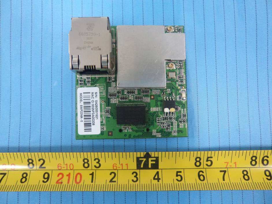
VZFSWP23MA
Sep 26, 2012802.11b/g/n (2T2R) WLAN AP/Router Module
Equipment Class
DTS - Digital Transmission System
VZFSWN21MB
Apr 26, 2012802.11 b/g/n WLAN USB Module
Equipment Class
DTS - Digital Transmission System