W7OMRF24J40MDMEIEEE 802.15.4 RF Transceiver Module
Microchip Technology Incorporated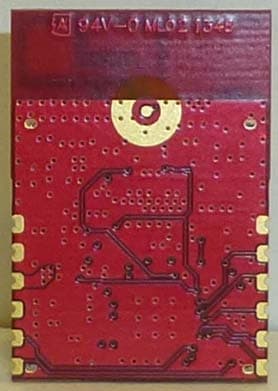
Click to zoom
Application Details
- Equipment Class
- DTS - Digital Transmission System
- Date of Grant
- Mar 05, 2014
- Application Purpose
- Original Equipment
- Date of Application
- Mar 05, 2014
- Equipment Note
- IEEE 802.15.4 RF Transceiver Module
- Frequency Range
- 2405.00000000 - 2475.00000000
- Country
- United States
Documents & Files
Document Text
Text extracted from the exhibit documents filed with the FCC. Open a document above to read the original.
Users Manual
2014 Microchip Technology Inc.PreliminaryDS7XXXXXXXA-page 1 MRF24J40MD/ME Features: • IEEE Std. 802.15.4™ Compliant RF Transceiver • Supports ZigBee ® , MiWi™ Development Environment Proprietary Wireless Networking Protocols • 4-Wire Serial Peripheral Interface (SPI) with Interrupt • Small size: 0.9" x 1.3" (22.9 mm x 33.0 mm), Surface Mountable: Pin Compatible with MRF24J40MB and MRF24J40MC • Integrated Crystal, Internal Voltage Regulator, Matching Circuitry, Power Amplifier, Low Noise Amplifier • PCB Antenna (MRF24J40MD), External Antenna Connector (MRF24J40ME): Ultra Miniature Coaxial (U.FL), 50Ω • Easy Integration into Final Product: Minimize Product Development, Quicker Time to Market • Compliance: - Modular Certified for the United States (FCC) and Canada (IC) - European R&TTE Directive Assessed Radio Module - Australia/New Zealand • Compatible with Microchip microcontroller families (PIC16, PIC18, PIC24, dsPIC33 and PIC32) • Range up to 4000 ft Operational: • Operating Voltage: 3.0V-3.6V (3.3V typical) • Temperature Range: -40°C to +85°C Industrial • Low-Current Consumption: - Rx Mode: 25 mA (typical) - Tx Mode: 77mA (typical) - Sleep: 10 A (typical) RF/Analog Features: • ISM Band 2.405 GHz-2.475 GHz Operation • Data Rate: 250 kbps • -104 dBm Typical Sensitivity with -23 dBm Maximum Input Level • +19 dBm Typical Output Power with 45 dB Tx Power Control Range • Integrated Low Phase Noise VCO, Frequency Synthesizer and PLL Loop Filter • Digital VCO and Filter Calibration • Integrated RSSI ADC and I/Q DACs • Integrated LDO • High Receiver RSSI Dynamic Range MAC/Baseband Features: • Hardware CSMA-CA Mechanism, Automatic ACK Response and FCS Check • Independent Beacon, Transmit and GTS FIFO • Supports all CCA modes and RSS/LQI • Automatic Packet Retransmit Capable • Hardware Security Engine (AES-128) with CTR, CCM and CBC-MAC modes • Supports Encryption and Decryption for MAC Sub layer and Upper Layer Pin Diagram: 2 3 4 5 6 1 7 V IN GND 8 9 10 RESET WAKE SDO SDI SCK CS NC GND INT 12 11GND 2.4 GHz IEEE Std. 802.15.4™ RF Transceiver Module with PA/LNA MRF24J40MD/ME DS7XXXXXXXA-page 2Preliminary 2014 Microchip Technology Inc. Table of Contents 1.0Device Overview .......................................................................................................................................................................... 3 2.0Circuit Description ...................................................................................................................................................................... 11 3.0Regulatory Approval ................................................................................................................................................................... 19 4.0Electrical Characteristics ........................................................................................................................................................... 25 Appendix A: Revision History............................................................................................................................................................... 27 The Microchip Web Site ....................................................................................................................................................................... 29 Customer Change Notification Service ................................................................................................................................................ 29 Product Identification System............................................................................................................................................................... 30 TO OUR VALUED CUSTOMERS It is our intention to provide our valued customers with the best documentation possible to ensure successful use of your Microchip products. To this end, we will continue to improve our publications to better suit your needs. Our publications will be refined and enhanced as new volumes and updates are introduced. If you have any questions or comments regarding this publication, please contact the Marketing Communications Department via E-mail at [email protected] or fax the Reader Response Form in the back of this data sheet to (480) 792-4150. We welcome your feedback. Most Current Data Sheet To obtain the most up-to-date version of this data sheet, please register at our Worldwide Web site at: http://www.microchip.com You can determine the version of a data sheet by examining its literature number found on the bottom outside corner of any page. The last character of the literature number is the version number, (e.g., DS30000A is version A of document DS30000). Errata An errata sheet, describing minor operational differences from the data sheet and recommended workarounds, may exist for current devices. As device/documentation issues become known to us, we will publish an errata sheet. The errata will specify the revision of silicon and revision of document to which it applies. To determine if an errata sheet exists for a particular device, please check with one of the following: • Microchip’s Worldwide Web site; http://www.microchip.com • Your local Microchip sales office (see last page) When contacting a sales office, please specify which device, revision of silicon and data sheet (include literature number) you are using. Customer Notification System Register on our web site at www.microchip.com to receive the most current information on all of our products. 2014 Microchip Technology Inc.PreliminaryDS7XXXXXXXA-page 3 MRF24J40MD/ME 1.0DEVICE OVERVIEW The MRF24J40MD/ME is a 2.4 GHz IEEE Std. 802.15.4™ compliant, surface mount module with integrated crystal, internal voltage regulator, matching circuitry, Power Amplifier (PA), Low Noise Amplifier (LNA) with PCB Trace Antenna (MRF24J40MD) or 50Ω external antenna connector (MRF24J40ME). The MRF24J40MD/ME module operates in the non- licensed 2.4 GHz frequency band. The …
Text truncated - open the document above for the full version.
Block Diagram
MRF24J40MD/ME Wireless Transceiver Module Block Diagram 20 MHz Crystal Oscillator 20 MHz U1 P A LNA U2 X1 U3 U4 enna (MD) ctor (ME) MRF24J40 2.4 GHz Transceiver IC RF Balun RF Switch RF Switch 24 GH SPI Port U5 U6 To Host Controller To PCB Trace Ant Or To U.FL Conne c Nt Cl ill 2 . 4 GH z Bandpass Filter P A PA U6 N o t e: C rysta l osc ill ator, VCO, IF, and other frequency generating circuitry is internal to the MRF24J40 IC. nal ource 2.405 – 2.480 GHz Exter Power S
External Photos
MRF24J40MD/MRF24J40ME Module External Photos Page 1 of 2 Top View MRF24J40MD/MRF24J40ME Module External Photos Page 2 of 2 Bottom View
ID Label/Location Info
MRF24J40MD/MRF24J40ME Module Label and Label Location Page 1 of 2 Bottom View Label will be silkscreened to bottom of PCB assembly. © 2014 Microchip Technology Inc. FCC ID: W7OMRF24J40MDME IC: 7693A-24J40MDME MRF24J40MD/MRF24J40ME Module Label and Label Location Page 2 of 2 Top View Model: MR Model number will be laser etched on RF shield on top of PCB assembly. Model: MRF24J40MD Model: MRF24J40ME
Internal Photos
MRF24J40MD/MRF24J40ME Module Internal Photos Page 1 of 2 Top View MRF24J40MD/MRF24J40ME Module Internal Photos Page 2 of 2 Bottom View
Operational Description
MRF24J40MD/ME Transceiver Module – Circuit Description The MRF24J40MD/ME module is built around the MRF24J40 RF transceiver IC (U2). This IC contains a standard SPI serial data interface to an external data source. The data source will typically be a microcontroller which may also support the application for the product that uses the module. The IC also includes a voltage regulator which provides regulated power to all of the internal circuits on the IC. Bypass capacitors are provided around the IC as needed. An external crystal at 20.000 MHz generates the clock for all of the digital circuitry on the IC. It also serves as a reference for the frequency synthesizer used to generate the RF carrier. This is the only clock source for the IC. The transmitter function of the IC takes the data from the external data source over the SPI interface, and creates packets per the IEEE 802.15.4 standard in the baseband processor. It has an RF signal source and modulator to create the 2.4 GHz RF output signal. The receiver function of the IC takes a signal into the IC and performs a down conversion to base band where the data is taken out of the incoming packets and passed to the external data unit over the SPI interface. After the MRF24J40 IC, a solid state switch (U3) connects the IC to a power amplifier (PA) (U6) for increasing the transmitter power or to a low noise amplifier (LNA) (U1) to increase the receiver sensitivity. The output of the PA and the input of the LNA go to a second switch (U4) to select which of these is connected to the antenna. The PA has input and output matching circuitry to match the impedance and to reduce harmonics. Bandpass filter U5 further filters and reduces any transmitted harmonics. The LNA also has impedance matching circuitry. At the interface from the second switch to the antenna, an external LC filter is provided to reduce harmonics and to match the impedance to the antenna connector J1.
RF Exposure Info
Certificates and reports shall not be reproduced except in full, without the written permission of H.B Compliance Solutions, LLC. Maximum Permissible Exposure Statement For the Microchip Technology Inc. IEEE 802.15.4 RF Transceiver Module with PA/LNA February 21, 2014 Prepared for: Microchip Technology Inc. 2355 W. Chandler Blvd. Chandler, Arizona 85224 Prepared By: H.B. Compliance Solutions 5005 S. Ash Avenue, Suite A-10 Tempe, Arizona 85282 Reviewed By: Hoosamuddin Bandukwala Cert # ATL-0062-E HBCS MPE Report # EMC_13052_2 Page 2 of 2 Prediction of MPE limit at a given distance Equation from page 18 of OET Bulletin 65, Edition 97-01 S = PG/4πR2 Where, S = power density (mW/cm2) P = output power at the antenna terminal (mW) G = gain of transmit antenna (numeric) R = distance from transmitting antenna (cm) Maximum peak output power at antenna input terminal = 20.6 (dBm) Maximum peak output power at antenna input terminal = 114.81 (mW) Antenna gain (typical) = 5 (dBi) Maximum antenna gain = 3.16 (numeric) Prediction distance = 200 (cm) Prediction frequency = 2405 (MHz) MPE limit for uncontrolled exposure at prediction frequency = 1.0 (mW/cm^2) Power density at prediction frequency = 0.07217 (mW/cm^2) To solve for the minimum mounting distance required; R = √ (PG/4πS) R = √ (114.81 x 3.16 / 4π x 0.07217) = 20 cm (Based on continuous transmission) END OF TEST REPORT
Schematics
1 1 2 2 3 3 4 4 5 5 6 6 DD CC BB AA Title Schematic Sheet 1 D. B. Author Revision :R1 Microchip Technology Inc. Date 1/23/2014 2:48:01 PMMRF24J40MD-R2 1-23-14.Sch Doc File 1/ Project MRF24J40 Module VDD NC7SZ125P5X 24 Vcc 5 GND 3 OE 1 U7 VDD CS CS SCK SDI INT WAKE SCK SDIINT WAKESDO SDO 33pF C6 1uF C5 0.01uF C10 0.1uF C4 0.01uF C2 1uF C9 33pF C3 0.01uF C7 33pF C1 GND 100pF C31 18pF C32 20M Hz X1 18pF C33 0.1uF C35 0.1uF C34 B1 1 GND 2 B2 3 Vc1 6 Vc2 4 A 5 U3RF3023TR7 4.7nH L2 4.7nH L5 0.5pF C22 1.8pF C19 VDD 0.5pF C20 3.0nH L4 B1 1 GND 2 B2 3 Vc1 6 Vc2 4 A 5 U4RF3023TR7 TXRX RX TX SS T12LN01 RFIN 2 GND 0 VDD 6 RFOUT 5 U1 NP C14 0.0R R10 33pF C29 NP C30 2450 BP15B100E GND 1 OUT 2 GND 3 IN 4 U5 SS T12LP17E VCC2 1 VCC1 2 RFIN 3 VREF 4 DET 5 RFOUT 6 GND 0 U6 33pF C23 0.2pF C27 6.8nH L10 8.2nH L8 1nF C17 1nF C181nF C15 1nF C16 0.1uF C11 2N7002P,215 Q2 BSS84 Q1 VDD 470k R1 RXTX J1-ME UFL Connector RX PA_ON PA_ON_R VDD 0.0R R2 0.0R R3-ME A1A i Po wer Net i 50 Ohm i Po wer Net i Po wer Net i Po wer Net i 50 Ohm i 50 Ohm i 50 Ohm i50 Ohm i50 Ohm i50 Ohm i 50 Ohm i 50 Ohm i 50 Ohm i 50 Ohm i 50 Ohm i50 Ohm i 50 Ohm i 50 Ohm i50 Ohm i 50 Ohm i 50 Ohm GND 1 RESET 2 WAKE 3 INT 4 SDI 5 SCK 6 SDO 7 CS 8 VIN 10 GND 11 GND 12 NC 9 M1 MRF24J40 Module Footprint RF Testpoint NC 1nF C37 1nF C38 2.2uF C26 5.6R R8 33pF C28 1pF C44 33pF C36 GND NP R9 NC GPIO4 10 GPIO5 9 GPIO1 8 GPIO0 7 GND 6 VDD 5 VDD 4 RFN 3 RFP 2 VDD 1 CS 20 SCK 19 SDI 18 SDO 17 INT 16 WAKE 15 GND 14 RESET 13 GPIO3 12 GPIO2 11 NC 30 NC 29 NC 28 NC 27 NC 26 GND 25 GND 24 NC 23 GND 22 VDD 21 LCAP 40 VDD 39 NC 38 VDD 37 GND 36 VDD 35 OSC1 34 OSC2 33 VDD 32 VDD 31 GND 41 U2 GND VDD GND GND GND VDD VDD VDD GND VDD VDD VDDVDD GND 100pF C42 GND NP R7 GNDGND GND GND GND GND GND GND 33pF C8 GND 1.5pF C21 1pF C24 2.7nH L6 GND GND GND RESET RESET 33pF C43 VDD 0.0R R4 0.0R R5 51R R6 PIA101 PIA102 COA1A PIC101 PIC102 COC1 PIC201 PIC202 COC2 PIC301 PIC302 COC3 PIC401 PIC402 COC4 PIC501 PIC502 COC5 PIC601 PIC602 COC6 PIC701 PIC702 COC7 PIC801 PIC802 COC8 PIC901 PIC902 COC9 PIC1001 PIC1002 COC10 PIC1101PIC1102 COC11 PIC1401 PIC1402 COC14 PIC1501 PIC1502 COC15 PIC1601 PIC1602 COC16 PIC1701 PIC1702 COC17 PIC1801 PIC1802 COC18 PIC1901 PIC1902 COC19 PIC2001PIC2002 COC20 PIC2101 PIC2102 COC21 PIC2201 PIC2202 COC22 PIC2301 PIC2302 COC23 PIC2401 PIC2402 COC24 PIC2601 PIC2602 COC26 PIC2701 PIC2702 COC27 PIC2801 PIC2802 COC28 PIC2901 PIC2902 COC29 PIC3001 PIC3002 COC30 PIC3101 PIC3102 COC31 PIC3201 PIC3202 COC32 PIC3301 PIC3302 COC33 PIC3401 PIC3402 COC34 PIC3501PIC3502 COC35 PIC3601 PIC3602 COC36 PIC3701PIC3702 COC37 PIC3801PIC3802 COC38 PIC4201 PIC4202 COC42 PIC4301 PIC4302 COC43 PIC4401 PIC4402 COC44 PIJ10ME01 PIJ10ME02 COJ10ME PIL201 PIL202 COL2 PIL401 PIL402 COL4 PIL501 PIL502 COL5 PIL601 PIL602 COL6 PIL801 PIL802 COL8 PIL1001 PIL1002 COL10 PIM101 PIM102 PIM103 PIM104 PIM105 PIM106PIM107 PIM108 PIM109 PIM1010 PIM1011 PIM1012 COM1 PIQ101 PIQ102 PIQ103 COQ1 PIQ201 PIQ202 PIQ203 COQ2 PIR101PIR102 COR1 PIR201PIR202 COR2 PIR30ME01 PIR30ME02 COR30ME PIR401PIR402 COR4 PIR501PIR502 COR5 PIR601 PIR602 COR6 PIR701PIR702 COR7 PIR801 PIR802 COR8 PIR901PIR902 COR9 PIR1001 PIR1002 COR10 PITP101 COTP1 PIU100 PIU102 PIU105 PIU106 COU1 PIU201 PIU202 PIU203 PIU204 PIU205 PIU206 PIU207 PIU208 PIU209 PIU2010 PIU2011PIU2012 PIU2013PIU2014PIU2015PIU2016PIU2017PIU2018 PIU2019PIU2020 PIU2021 PIU2022 PIU2023 PIU2024 PIU2025 PIU2026 PIU2027 PIU2028 PIU2029 PIU2030 PIU2031PIU2032PIU2033PIU2034PIU2035PIU2036PIU2037PIU2038PIU2039PIU2040PIU2041 COU2 PIU301 PIU302 PIU303 PIU304 PIU305 PIU306 COU3 PIU401 PIU402 PIU403 PIU404 PIU405 PIU406 COU4 PIU501 PIU502 PIU503 PIU504 COU5 PIU600 PIU601 PIU602 PIU603 PIU604PIU605 PIU606 COU6 PIU701 PIU702 PIU703 PIU704 PIU705 COU7 PIX101 PIX102 PIX103 PIX104 COX1 PIM108 PIU2020 PIU701 NLC\S\ PIA102 PIC101 PIC201 PIC301PIC401 PIC501 PIC601 PIC701 PIC801PIC901 PIC1001 PIC1102 PIC1402 PIC1501PIC1601 PIC1701PIC1801 PIC2102 PIC2201 PIC2402 PIC2601 PIC2701 PIC3001 PIC3102 PIC3201PIC3301 PIC3401 PIC3501 PIC3702 PIC3802 PIC4201 PIC4301 PIC4401 PIJ10ME02 PIM101 PIM1011 PIM1012 PIQ202 PIR702 PIR901 PIU100 PIU206 PIU2014 PIU2022 PIU2024 PIU2025 PIU2036PIU2041 PIU302 PIU402 PIU501PIU503 PIU600 PIU703 PIX102PIX104 PIM104 PIU2016 NLINT PIM109 NLNC PIA101 PIR202 PIC1101 PIQ103 PIU106 PIC1401 PIR501 PIU403 PIC1901 PIU305 PIC1902PIC2002 PIL402 PIC2001 PIL201 PIL502 PIU202 PIC2101 PIL602 PIU405 PIC2202 PIL401PIL501 PIU203 PIC2301 PIR602 PIC2302 PIU303 PIC2401 PIC3602 PIL601 PIC2702 PIL801 PIL1002 PIC2801 PIU502 PIC2802 PIR701 PIR801 PIC2901 PIC3002 PIU504 PIC2902 PIU606 PIC3101 PIU2040 PIC3202 PIU2034 PIX101 PIC3302 PIU2033 PIX103 PIC3601 PIR201 PIR30ME02 PITP101 PIC4402 PIR401PIU105 PIJ10ME01 PIR30ME01 PIL802 PIR601 PIL1001 PIU603 PIM107PIU704 PIQ101 PIQ203 PIR102 PIR402 PIU301 PIR502PIU102 PIR802 PIR902 PIR1001 PIR1002 PIU401 PIU209 PIU2010 PIU2012 PIU2023 PIU2026 PIU2027 PIU2028 PIU2029 PIU2030 PIU2038 PIU605 PIC4202 PIU207 PIU604 NLPA0ON NLPA0ON0R PIM102 PIU2013 NLR\E\S\E\T\ PIC1602 PIC1802 PIQ201 PIU2011 PIU304 PIU406 NLRX PIM106 PIU2019 NLSCK PIM105 PIU2018 NLSDI PIU2017 PIU702 NLSDO PIC1502 PIC1702 PIU208 PIU306 PIU404 NLTX PIC102 PIC202 PIC302PIC402 PIC502 PIC602 PIC702 PIC802PIC902PIC1002 PIC2602 PIC3402 PIC3502 PIC3701 PIC3801 PIC4302 PIL202 PIM1010 PIQ102 PIR101 PIU201 PIU204 PIU205 PIU2021 PIU2031PIU2032PIU2035PIU2037PIU2039 PIU601 PIU602 PIU705 NLVDD PIM103 PIU2015 NLWAKE
Test Report
Certificates and reports shall not be reproduced except in full, without the written permission of H.B Compliance Solutions, LLC. Intentional Radiator Test Report For the Microchip Technology Inc. IEEE 802.15.4 RF Transceiver Module with PA/LNA Tested under The FCC Rules contained in Title 47 of the CFR, Part 15.247 for Digitally Transmitting Sequence Prepared for: Microchip Technology Inc. 2355 W. Chandler Blvd. Chandler, AZ 85224 Prepared By: H.B. Compliance Solutions 5005 S. Ash Avenue, Suite # A-10 Tempe, Arizona 85282 Reviewed By: Hoosamuddin Bandukwala Cert # ATL-0062-E Engineering Statement: The measurements shown in this report were made in accordance with the procedure indicated, and the emissions from this equipment were found to be within the limits applicable. I assume full responsibility for the accuracy and completeness of these measurements, and for the qualifications of all persons taking them. It is further stated that upon the basis of the measurement made, the equipment tested is capable of operation in accordance with the requirements of Part 15 of the FCC Rules under normal use and maintenance. HBCS Report # EMC_13052_1 Page 2 of 37 Report Status Sheet Revision # Report Date Reason for Revision Ø February 20, 2014 Initial Issue 1 March 4, 2014 Update references and channel info. HBCS Report # EMC_13052_1 Page 3 of 37 Table of Contents EXECUTIVE SUMMARY ............................................................................................ 4 1. Testing Summary ........................................................................................ 4 EQUIPMENT CONFIGURATION ................................................................................ 5 1. Overview .................................................................................................... 5 2. Test Facility ................................................................................................. 6 3. Description of Test Sample ......................................................................... 6 4. Equipment Configuration ........................................................................... 6 5. Support Equipment .................................................................................... 7 6. Ports and Cabling Information .................................................................... 7 7. Method of Monitoring EUT Operation ........................................................ 7 8. Mode of Operation ..................................................................................... 7 9. Modifications ............................................................................................. 8 10. Disposition of EUT ...................................................................................... 8 Criteria for Un-Intentional Radiators ...................................................................... 9 1. Radiated Emissions ..................................................................................... 9 Emissions Tests Calculations ...................................................................... 10 Criteria for Intentional Radiators .......................................................................... 13 2. Conducted Emissions ................................................................................ 13 1. Occupied Bandwidth ................................................................................ 16 2. RF Power Output ...................................................................................... 19 3. Conducted Spurious Emissions ................................................................. 22 4. Radiated Spurious Emissions and Restricted Band ................................... 27 6. Emissions At Band Edges .......................................................................... 32 7. Power Spectral Density ............................................................................. 34 I. Test Equipment ............................................................................................. 37 HBCS Report # EMC_13052_1 Page 4 of 37 EXECUTIVE SUMMARY 1. Testing Summary These tests were conducted on a sample of the equipment for the purpose of demonstrating compliance with Part 15.247. All tests were conducted using measurement procedure from ANSI C63.10-2009 and FCC DTS Measurement Guidance KDB558074 v03r01 April 09, 2013 as appropriate. Test Name Test Method/Standard Result Comments Unintentional Radiated Emissions 15.109 Pass A/C Powerline Conducted Emissions 15.207 Pass Occupied Bandwidth 15.247(a)(2) Pass Peak Output Power 15.247(b) Pass Conducted Spurious Emissions 15.247(d) Pass Radiated Spurious Emissions & Restricted Band 15.247(d), 15.209(a), 15.205 Pass Emissions At Band Edges 15.247(d), 15.209(a), 15.205 Pass Power Spectral Density 15.247(e) Pass HBCS Report # EMC_13052_1 Page 5 of 37 EQUIPMENT CONFIGURATION 1. Overview H.B Compliance Solutions was contracted by Microchip Technology Inc. to perform testing on the IEEE 802.15.4 RF Transceiver module under the purchase order number 209594. This document describes the test setups, test methods, required test equipment, and the test limit criteria used to perform compliance testing of the Microchip Technology Inc., IEEE 802.15.4 RF Transceiver module. The tests were based on FCC Part 15 Rules. The tests described in this document were formal tests as described with the objective of the testing was to evaluate compliance of the Equipment Under Test (EUT) to the requirements of the aforementioned specifications. Microchip Technology should retain a copy of this document and it should be kept on file for at least five years after the manufacturing of the EUT has been permanently discontinued. The results obtained relate only to the item(s) tested. Product Name: IEEE 802.15.4 RF Transceiver module with PA/LNA Model(s) Tested: MRF24J40MD & MRF24J40ME FCC ID: W70-MRF24J40MDME Supply Voltage Input: Primary Power : 3.3 Vdc Frequency Rang…
Text truncated - open the document above for the full version.
Test Setup Photos
Test Setup Photo 1 Test Setup Photo 2 Test Setup Photo 3 Test Setup Photo 4 Test Setup Photo 5
Contact Information
Applicant
Steve Caldwell(Director, Wireless Product Division)
Technical Contact
Microchip TechnologySteven Bible
[email protected]4807924298
2355 W. Chandler Blvd. · Chandler, Arizona · United States
Test Firm
SMART EC Product Testing ServicesTeresa Kaczmarowski
[email protected]602 437 6898
Technical Specifications
| # | Rule Parts | Frequency Range | Power Output |
|---|---|---|---|
| 1 | 15C | 2.40 GHz - 2.48 GHz | 115.00 mW |
Other Applications from Microchip Technology Incorporated
W7O24WN0
Aug 26, 2015802.11BGN 1X1 MODULE
Equipment Class
DTS - Digital Transmission System
W7OMRF24WG0MAMB
Aug 30, 2012802.11b/g Radio Card
Equipment Class
DTS - Digital Transmission System