W7OMRF24WG0MAMB802.11b/g Radio Card
Microchip Technology Incorporated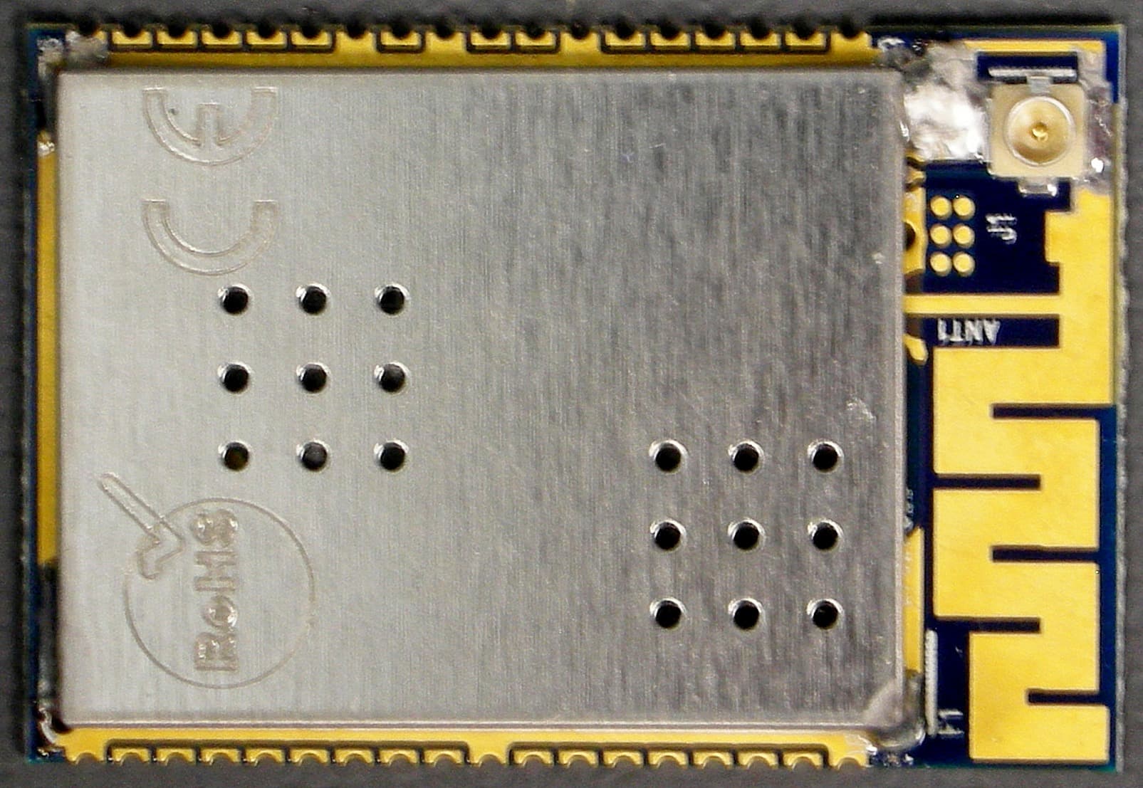
Click to zoom
Application Details
- Equipment Class
- DTS - Digital Transmission System
- Date of Grant
- Aug 30, 2012
- Application Purpose
- Original Equipment
- Date of Application
- Aug 30, 2012
- Equipment Note
- 802.11b/g Radio Card
- Frequency Range
- 2412.00000000 - 2462.00000000
- Country
- United States
Documents & Files
Document Text
Text extracted from the exhibit documents filed with the FCC. Open a document above to read the original.
Users Manual
2012 Microchip Technology Inc.Advance InformationDS00000A-page 1 MRF24WG0MA/MB Features: • IEEE 802.11-compliant RF transceiver • Serialized unique MAC address • Data rate: 1 to 11 Mbps for 802.11b / 6 to 54 Mbps for 802.11g • Compatible with IEEE 802.11b/g/n networks • Small size: 21 mm x 31 mm 36-pin Surface Mount module • Integrated PCB antenna (MRF24WG0MA) • External antenna option (MRF24WG0MB) with ultra-miniature coaxial (U.FL) connector • Easy integration into final product – accelerates product development, provides quicker time to market • Radio regulation certification for United States (FCC), Canada (IC), and Europe (ETSI) • Designed for use with Microchip microcontroller families (PIC18, PIC24, dsPIC33, and PIC32) with downloadable Microchip TCP/IP Stack Operational: • Single operating voltage: 2.8V to 3.6V (3.3V typical) • Temperature range: -40°C to +85°C • Simple, four-wire SPI interface with interrupt • Low-current consumption: - RX mode – 95 mA (typical) - TX mode – 240 mA (+18 dBm typical) - PS mode – 4 mA (typical) - Hibernate mode – 0.1 mA (typical) RF/Analog Features: • ISM Band 2.400 to 2.484 GHz operation • 14 Channels selectable individually or domain- restricted • DSSS/OFDM modulation • Application throughput: 4500 kbps • -95 dBm Typical sensitivity at 1 Mbps • +18 dBm Typical 802.11b TX power with control • +16 dBm Typical 802.11g TX power with control • Integrated low phase noise VCO, RF frequency synthesizer, PLL loop filter and PA • Integrated RSSI ADC and I/Q DACs, RSSI readings available to host MAC/Baseband Features: • Hardware CSMA/CA access control, automatic ACK, and FCS creation and checking • Automatic MAC packet retransmit • Hardware Security Engine for AES and RC4-based ciphers • Supports 802.1x, 802.1i security: WEP, WPA-PSK, and WPA-2-PSK. Applications: • Utility and Smart Energy: - Thermostats - Smart Meters - White Goods -HVAC • Consumer Electronics: - Remote Control - Internet Radio - Home Security -Toys • Industrial Controls: - Chemical Sensors -HVAC - Security Systems - M2M Communication • Remote Device Management: - Location and Asset Tracking - Automotive - Code Update • Retail: - POS Terminals - Wireless Price Tags - Digital Remote • Medical, Fitness, and Health Care: - Glucose Meters - Fitness Equipment - Patient Asset Tracking MRF24WG0MA/MB Data Sheet 2.4 GHz IEEE 802.11b/g™ MRF24WG0MA/MB DS00000A-page 2Advance Information 2012 Microchip Technology Inc. Pin Diagram Note:Antenna connector on MRF24WG0MB only. 2012 Microchip Technology Inc.Advance InformationDS00000A-page 3 MRF24WG0MA/MB Table of Contents 1.0Device Overview .......................................................................................................................................................................... 5 2.0Circuit Description ...................................................................................................................................................................... 11 3.0Regulatory Approval................................................................................................................................................................... 21 4.0Electrical Characteristics ............................................................................................................................................................ 27 Appendix A: Revision History............................................................................................................................................................... 31 The Microchip Web Site ....................................................................................................................................................................... 33 Customer Change Notification Service ................................................................................................................................................ 33 Customer Support ................................................................................................................................................................................ 33 Reader Response ................................................................................................................................................................................ 34 Product Identification System .............................................................................................................................................................. 35 TO OUR VALUED CUSTOMERS It is our intention to provide our valued customers with the best documentation possible to ensure successful use of your Microchip products. To this end, we will continue to improve our publications to better suit your needs. Our publications will be refined and enhanced as new volumes and updates are introduced. If you have any questions or comments regarding this publication, please contact the Marketing Communications Department via E-mail at [email protected] or fax the Reader Response Form in the back of this data sheet to (480) 792-4150. We welcome your feedback. Most Current Data Sheet To obtain the most up-to-date version of this data sheet, please register at our Worldwide Web site at: http://www.microchip.com You can determine the version of a data sheet by examining its literature number found on the bottom outside corner of any page. The last character of the literature number is the version number, (e.g., DS30000A is version A of document DS30000). Errata An errata sheet, describing minor operational differences from the data sheet and recommended workarounds, may exist for current devices. As device/documentation issues become known to us, we will publish an errata sheet. The errata will specify the revision of silicon and revision of document to which it applies. To determine if an errata sheet exists for a particular device, please check with one of the following: • Microchip’s Worldwide Web site; http://ww…
Text truncated - open the document above for the full version.
Block Diagram
MRF24WG0MAMB Transceiver Module – Block Diagram MRF24WG0 MAC/Baseband IC SPI Interface Baseband packet Processing Voltage 40MHz tx rx ctl Regulator Antenna Matching Circuitry 40.0000 MHz crystal External data source External Power source PCB Antenna J1 PCB Ante nna AL2236 transceiver IC RF generation and reception Voltage Regulator External Antenna Option
Cover Letter(s)
Applicant/Grantee Microchip Technology Incorporated FCC ID: W70MRF24WG0MAMB Section 15.212 Modular Transmitters Request for Modular Approval Request for Limited Modular Approval Requirements EUT Conditions Comply (Y/N) Single Modular Approval Requirements 1 The radio elements of the modular transmitter must have their own shielding. The physical crystal and tuning capacitors may be located external to the shielded radio elements. Y 2 The modular transmitter must have buffered modulation/data inputs (if such inputs are provided) to ensure that the module will comply with Part 15 requirements under conditions of excessive data rates or over-modulation. Y 3 The modular transmitter must have its own power supply regulation. Y 4 The modular transmitter must comply with the antenna and transmission system requirements of Sections 15.203, 15.204(b) and 15.204(c). The antenna must either be permanently attached or employ a “unique” antenna coupler (at all connections between the module and the antenna, including the cable). The “professional installation” provision of Section 15.203 is not applicable to modules but can apply to limited modular approvals under paragraph (b) of this section. Y 5 The modular transmitter must be tested in a stand-alone configuration, i.e., the module must not be inside another device during testing for compliance with Part 15 requirements. Unless the transmitter module will be battery powered, it must comply with the AC line conducted requirements found in Section 15.207. AC or DC power lines and data input/output lines connected to the module must not contain ferrites, unless they will be marketed with the module (see Section 15.27(a)). The length of these lines shall be the length typical of actual use or, if that length is unknown, at least 10 centimeters to insure that there is no coupling between the case of the module and supporting Y equipment. Any accessories, peripherals, or support equipment connected to the module during testing shall be unmodified and commercially available (see Section 15.31(i)). 6 The modular transmitter must be equipped with either a permanently affixed label or must be capable of electronically displaying its FCC identification number. (A) If using a permanently affixed label, the modular transmitter must be labeled with its own FCC identification number, and, if the FCC identification number is not visible when the module is installed inside another device, then the outside of the device into which the module is installed must also display a label referring to the enclosed module. This exterior label can use wording such as the following: “Contains Transmitter Module FCC ID: XYZMODEL1” or “Contains FCC ID: XYZMODEL1.” Any similar wording that expresses the same meaning may be used. The Grantee may either provide such a label, an example of which must be included in the application for equipment authorization, or, must provide adequate instructions along with the module which explain this requirement. In the latter case, a copy of these instructions must be included in the application for equipment authorization. (B) If the modular transmitter uses an electronic display of the FCC identification number, the information must be readily accessible and visible on the modular transmitter or on the device in which it is installed. If the module is installed inside another device, then the outside of the device into which the module is installed must display a label referring to the enclosed module. This exterior label can use wording such as the following: “Contains FCC certified transmitter module(s).” Any similar wording that expresses the same meaning may be used. The user manual must include instructions on how to access the electronic display. A copy of these instructions must be included in the application for equipment authorization. Y 7 The modular transmitter must comply with any specific rules or operating requirements that ordinarily apply to a complete transmitter and the manufacturer must provide adequate instructions along with the module to explain any such requirements. A copy of these instructions must be included in the application for equipment authorization. Y 8 The modular transmitter must comply with any applicable RF exposure requirements in its final configuration. Y A limited modular approval may be granted for single or split modular transmitters that do not comply with all of the above requirements, e.g., shielding, minimum signaling amplitude, buffered modulation/data inputs, or power supply regulation, if the manufacturer can demonstrate by alternative means in the application for equipment authorization that the modular transmitter meets all the applicable Part 15 requirements under the operating conditions in which the transmitter will be used. Limited modular approval also may be granted in those instances where compliance with RF exposure rules is demonstrated only for particular product configurations. The applicant for certification must state how control of the end product into which the module will be installed will be maintained such that full compliance of the end product is always ensured.
Operational Description
MRF24WG0MAMB Transceiver Module – Circuit Description The MRF24WG0MAMB module is built around the MRF24WG0 MAC/Baseband IC and AL2236 RF transceiver IC. The WBAA1 MAC/Baseband IC contains a standard SPI serial data interface to an external data source. The data source will typically be a microcontroller which may also support the application for the product that uses the module. The IC also includes a voltage regulator which provides regulated power to all of the internal circuits on the IC. Bypass capacitors are provided around the IC as needed. An external crystal at 40.0000 MHz generates the clock for all of the digital circuitry on the IC. It also serves as a reference for the frequency synthesizer used to generate the RF carrier. This is the only clock source for the IC. The transmitter function of the MRF24WG0 MAC/Baseband IC takes the data from the external data source over the SPI interface and creates packets in the MAC and baseband processor. In conjunction with the AL2236 RF transceiver, it generates an RF signal source and modulator to create the 2412 - 2484 MHz RF output signal. The receiver function of the AL2236 RF transceiver down converts the RF signal to baseband where the data is taken out of the incoming packets by the MAC and passed to the external data unit over the SPI interface. There are two versions of this module, one that is configured with an integrated PCB antenna, distinguished as Model: MRF24WG0MA and the other is configured to use an external antenna distinguished as Model: MRF24WG0MB. The antenna output of the MRF24WG0MA is impedance matched to a fixed PCB antenna. The external antenna option on the MRF24WG0MB connects the Rx/Tx output to external connector J1.
Parts List/Tune Up Info
8F, No.63, Juguang Rd, Zhonghe Dist, New Taipei City 235, Taiwan, R.O.C. Tel : +886-2-2225-8209 Fax: +886-2-2225-7523 www.aristotle.com.tw RFA-02-C2M2-D034 Specifications Frequency range 2400 MHz – 2500 MHz Antenna gain 2 dBi VSWR 2.0 : 1 Max. Polarization Linear, vertical Impedance 50 Ω Temperature - 10°C to +55°C Connector R SMA PLUG
Parts List/Tune Up Info
8F, No.63, Juguang Rd, Zhonghe Dist, New Taipei City 235, Taiwan, R.O.C. Tel : +886-2-2225-8209 Fax: +886-2-2225-7523 www.aristotle.com.tw RFA-02-G03-D034 Electrical Specifications Frequency range 2400 MHz – 2500 MHz VSWR 2.0 : 1 Max. Polarization Linear, vertical Power handling 1W (cw) Impedance 50 Ω Connector I-PEX Cable Ø1.13mm Environmental & Mechanical Characteristics Temperature - 10°C to +55°C Humidity 95% @ 25°C
Parts List/Tune Up Info
8F, No.63, Juguang Rd, Zhonghe Dist, New Taipei City 235, Taiwan, R.O.C. Tel : +886-2-2225-8209 Fax: +886-2-2225-7523 www.aristotle.com.tw RFA-02-P05-D034 Electrical Specifications Frequency range 2400 MHz – 2500 MHz Peak Gain 2 dBi Average gain 1 dBi VSWR 2.0 : 1 Max. Polarization Linear, vertical Power handling 1W (cw) Impedance 50 Ω Connector I-PEX Cable Ø1.13mm Environmental & Mechanical Characteristics Temperature - 10°C to +55°C Humidity 95% @ 25°C
RF Exposure Info
FCC Part 1 Subpart I FCC Part 2 Subpart J INDUSTRY CANADA RSS 102 ISSUE 3 RF EXPOSURE REPORT FOR 802.11b/g RADIO CARD- 4 TYPES OF ANTENNAS (INTEGRAL, DIPOLE, PCBA, AND PIFA) FCC ID: W7OMRF24WG0MAMB FCC MODEL NUMBER: MRF24WG0MAMB IC NUMBER: 7693A-24W0MAMB IC MODEL: MRF24WG0MA, MRF24WG0MB REPORT NUMBER: 12U14434-5 ISSUE DATE: AUGUST 3, 2012 Prepared for MICROCHIP TECHNOLOGY, INC. 2355 West Chandler Blvd Chandler, AZ 85224-6199, USA Prepared by UL CCS 47173 BENICIA STREET FREMONT, CA 94538, U.S.A. TEL: (510) 771-1000 FAX: (510) 661-0888 REPORT NO: 12U14434-5 DATE: AUG 3, 2012 FCC ID: W7OMRF24WG0MAMB IC: 7693A-24W0MAMB Page 2 of 10 UL CCS FORM NO: CCSUP4701G 47173 BENICIA STREET, FREMONT, CA 94538, USA TEL: (510) 771-1000 FAX: (510) 661-0888 This report shall not be reproduced except in full, without the written approval of UL CCS. Revision History Rev. Issue Date Revisions Revised By -- 08/03/12 Initial Issue T. LEE REPORT NO: 12U14434-5 DATE: AUG 3, 2012 FCC ID: W7OMRF24WG0MAMB IC: 7693A-24W0MAMB Page 3 of 10 UL CCS FORM NO: CCSUP4701G 47173 BENICIA STREET, FREMONT, CA 94538, USA TEL: (510) 771-1000 FAX: (510) 661-0888 This report shall not be reproduced except in full, without the written approval of UL CCS. TABLE OF CONTENTS 1. ATTESTATION OF TEST RESULTS .................................................................................... 4 2. METHODOLOGY .................................................................................................................. 5 3. REFERENCES ...................................................................................................................... 5 4. FACILITIES AND ACCREDITATION .................................................................................... 5 5. EUT DESCRIPTION .............................................................................................................. 5 6. REQUIREMENTS - LIMITATION OF EXPOSURE ............................................................... 6 6.1. LIMITS ........................................................................................................................... 6 6.1.1. FCC RULES .......................................................................................................... 6 6.1.2. IC RULES .............................................................................................................. 7 6.1.3. LIMITS APPLICABLE TO THE EUT...................... Error! Bookmark not defined. 6.2. EQUATIONS ................................................................................................................. 8 6.3. RESULTS ...................................................................................................................... 9 REPORT NO: 12U14434-5 DATE: AUG 3, 2012 FCC ID: W7OMRF24WG0MAMB IC: 7693A-24W0MAMB Page 4 of 10 UL CCS FORM NO: CCSUP4701G 47173 BENICIA STREET, FREMONT, CA 94538, USA TEL: (510) 771-1000 FAX: (510) 661-0888 This report shall not be reproduced except in full, without the written approval of UL CCS. 1. ATTESTATION OF TEST RESULTS COMPANY NAME: MICROCHIP TECHNOLOGY, INC. 2355 West Chandler Blvd Chandler, AZ 85224-6199, USA EUT DESCRIPTION: 802.11b/g RADIO CARD- 4 TYPES OF ANTENNAS (INTEGRAL, DIPOLE, PCBA, AND PIFA) FCC MODELS: MRF24WG0MAMB IC MODELS: MRF24WG0MA, MRF24WG0MB APPLICABLE STANDARDS STANDARD TEST RESULTS FCC PART 1 SUBPART I & PART 2 SUBPART J Pass INDUSTRY CANADA RSS 102 ISSUE 3 Pass UL CCS calculated the RF Exposure of the above equipment in accordance with the requirements set forth in the above standards, using test results reported in the test report documents referenced below and/or documentation furnished by the applicant. All indications of Pass/Fail in this report are opinions expressed by UL CCS based on interpretations of these calculations. The results show that the equipment is capable of demonstrating compliance with the requirements as documented in this report. Note: The results documented in this report apply only to the tested sample, under the conditions and modes of operation, as described by the referenced documents. This document may not be altered or revised in any way unless done so by UL CCS and all revisions are duly noted in the revisions section. Any alteration of this document not carried out by UL CCS will constitute fraud and shall nullify the document. This report must not be used by the client to claim product certification, approval, or endorsement by NVLAP, NIST, any agency of the Federal Government, or any agency of any government. Approved & Released For UL CCS By: Calculated By: TIM LEE DOUG ANDERSON STAFF ENGINEER EMC ENGINEER UL CCS UL CCS REPORT NO: 12U14434-5 DATE: AUG 3, 2012 FCC ID: W7OMRF24WG0MAMB IC: 7693A-24W0MAMB Page 5 of 10 UL CCS FORM NO: CCSUP4701G 47173 BENICIA STREET, FREMONT, CA 94538, USA TEL: (510) 771-1000 FAX: (510) 661-0888 This report shall not be reproduced except in full, without the written approval of UL CCS. 2. METHODOLOGY All calculations were made in accordance with FCC OET Bulletin 65 Edition 97-01 and IC Safety Code 6. 3. REFERENCES All measurements were made as documented in test report UL CCS Test Report 12U14434-1C for operation in the 2.4 GHz and 5 GHz bands. Output power, Duty cycle and Antenna gain data is excerpted from the applicable test reports. Antenna gain data is excerpted from product documentation provided by the applicant. 4. FACILITIES AND ACCREDITATION The test sites and measurement facilities used to collect data are located at 47173 Benicia Street, Fremont, California, USA. UL CCS is accredited by NVLAP, Laboratory Code 200065-0. The full scope of accreditation can be viewed at http://www.ccsemc.com. 5. EUT DESCRIPTION The EUT is an 802.11b/g transceiver module. Other details regarding the EUT are documented in the applicable test reports and product documentation. REPORT NO: 12U14434-5 DATE: AUG 3, 2012 FCC ID: W7OMRF24WG0MAMB IC: 7693A-24W0MAMB Page 6 of 10 UL CCS FORM NO: CCSUP4701G 47173 BENICIA STREET, FRE…
Text truncated - open the document above for the full version.
Schematics
REV A DESIGN IS RELEASED TO LAYOUT 12/25/2010 B MCHP11-0094-B 03/10/201203/05/201203/05/201202/29/2012 ROBEFE DEL ROSARIORICK MODDY REV A REV 0 MODULE5x5-QFH-G3k_AIROHA-x1 14-A5147 3 11/11/2010 C ECO NO: LTR APPROVED BY: REVISION RECORD SPEC #:DEVICE ID: REVISION HISTORY REV 0 INITIAL SCHEMATIC DEVELOPED FOR SCHEMATIC KICK OFF REV: NOTES: DATE: DESIGN SPECIFIC NOTES DATE: 88/88/8888 14-A8888-XX XX XXXXX XXXXXXX 14-A5147 -03.SCH MICROCHIP TECHNOLOGY INC. DRAWING #: SIZE: RELEASED:CHECKED:DRAWN: DATE: SPEC #:FILE NAME: REV: TITLE:COMPANY: DATE:DATE:DATE: SHEET: OF 14-A5147 5 4321 F E D C B A F E 654321 D C B A ROBEFE DEL ROSARIOSirooj Rambaran PEER REVIEW BY: The information contained in this file is considered confidential and proprietary to Microchip Technology, Inc.as covered in our Non Disclosure Agreement. This information shall not be shared with any other party. MRF24WG0MA/MB/MC 1 GND NC RESET GND SDI SCK INT SDONCGNDVDDGNDDEBUG_TXDEBUG_RXGNDNCCSTEST_0NCHIBERNATEGND JTAG_TDO JTAG_TCK JTAG_TMS JTAG_TDI HW_STRAP JTAG_RST NC GND GPIO_3GPIO_2GPIO_1GPIO_0 WP VDD GND 1 2 3 456789 101112131415161718 36 35 34 333231302928272625242322212019 RF SHIELD MODULE CUSTOMER BOARD PCB STACK UP (FR4) 1.5oz Cu LAYER 1 LAYER 2LAYER 3LATER 4 1. All parts must be placed only on the TOP Antenna area No copper Keepout Area No components 1.0oz Cu1.0oz Cu1.5oz Cu J1 Initial released ADDITIONAL CIRCUITS IN THE SCHEMATIC 02/29/2012 REVB UPDATE PCB WITH RESPECT TO SCHEMATIC MODIFICATION REVB RF SHIELD F F 654321 E D C B A C -03.SCH DRAWING #: SIZE: RELEASED: DRAWN: SPEC #:FILE NAME: DATE:DATE: SHEET: OF 14-A5147 5 4321 ROBEFE DEL ROSARIO 03/05/2012 03/10/2012 3 MCHP11-0094-B 14-A5147 ROBEFE DEL ROSARIO 2 E D C B A TITLE: REV: B MRF24WG0MA/MB/MC PLACE CRYSTAL AS CLOSE AS POSSIBLE TO G3K Do not install Donot install 1 VSSIO 2 VDDIO 3 RF_TX_EN 4 RF_RX_EN 5 RF_RADIO_EN 6 RF_PA_EN 7 VSS 8 VDD12 9 RF_GAIN1 10 RF_GAIN2 11 RF_GAIN3 12 RF_GAIN4 13 RF_GAIN5 14 RF_GAIN6 15 RF_GAIN7 16 VSS 17 VSS_ANA 18 CE_N 19 RXIP 20 RXIN 21 VSS_ANA 66 VSS_IO 65 VDDIO 64 SS_N 63 SI 62 SO 61 SCK 60 VSS 59 VDD12 58 GPIO0 57 GPIO1 56 GPIO2 55 GPIO3 54 RF_CSN 53 INTR_N 52 TIMER_TEST 51 TIMER_CAP 50 VSS_EXT 49 LDO_12_DIG 48 VDD_33_DIG 47 VDD_33_TX 46 LDO_28 45 BFC28_VSS_TX 67 HW_STRAP 68 JTAG_RST 69 JTAG_TDI 70 JTAG_TMS 71 JTAG_TCK 72 JTAG_TDO 73 VSS 74 VDD12 75 TEST_0 76 UART_RX 77 UART_TX 78 U_RTS 79 U_CTS 80 RST_N 81 RF_HP_EN 44 TXIP 43 TXIN 42 VSS_TX 41 VDD_12_TX 40 TXQP 39 TXQN 38 BG 37 VSS_PLL 36 VDD_33_PLL 35 ATB 34 VSS_PLL 33 LDO_12_PLL 32 OSCOUT 31 XTALO 30 XTALI 29 VSS_PLL 28 PLL_TEST_VSS_PLL 27 VSS_ANA 26 LDO_12_ANA 25 VDD_33_ANA 24 PA_DET 23 RX_QN 22 RXQP U4 ICL_G3000_LGA5X5_81L_X C32 4.7uF C334.7uF C3510uF C3610uF C3710uF C5210uF C531uF C544.7uF R5 4.75K GND Y1 R2 4.75K C3 4.7uF R6 4.75K 1 CS 2 SO 3 WP 4 GND 8 VCC 7 HOLD 6 SCK 5 SI U3 ICL_SST25VF020B_WSON_8L_X JTAG_TDO(3) JTAG_TCK(4) JTAG_TMS(5) JTAG_TDI(6) JTAG_RST(9) HW_STRAP(8) TP1 GND(1) VDD(17) RESET(7) HIBERNATE(20) DEBUG_RX(26) DEBUG_TX(27) CS(23) SDI(35) SDO(32) SCK(34) INT(33) VDD(29) GND(10) GND(18) GND(19) GND(25) GND(28) GND(30) GND(36) C12 3.6pF C13 3.6pF C14 3.6pF C213.6pF C24 3.6pF TP2 TP3 R1 4.75K WP(16) TP4 NC(2) NC(11) GPIO_3(12) GPIO_1(14) GPIO_0(15) NC(21) TEST_0(22) NC(24) NC(31) R9 0.0 R10 0.0 R11 0.0 C9 0.1uF C15 0.1uF L7 56nH C18 0.1uF C34 0.1uF L8 56nH GPIO_2(13) L3 56nH C4110uF VDD VCC_2V8 A_TXON A_RXON A_PLLON A_PAON A_GC1 A_GC2A_GC3A_GC4 A_GC5A_GC6 A_GC7 A_RX_IP A_RX_IN A_RX_QP A_RX_QN A_TX_IPA_TX_INA_TX_QPA_TX_QN A_PDOUT A_RXHP_TXBG A_GPIO_0A_GPIO_2 OSC_OUT A_GPIO_1A_GPIO_3 A_RF_CSN VDD VDD A_GPIO_2 A_GPIO_3A_GPIO_1 A_GPIO_0 VDD VDD VDD TITLE: A B C D E 3 ROBEFE DEL ROSARIO 14-A5147 MCHP11-0094-B 3 03/10/201203/05/2012 ROBEFE DEL ROSARIO 1 2 3 4 5 14-A5147 OF SHEET: DATE:DATE: FILE NAME:SPEC #: DRAWN: RELEASED: SIZE: DRAWING #: -03.SCH C A B C D E as covered in our Non Disclosure Agreement. This information shall not be shared with any other party.The information contained in this file is considered confidential and proprietary to Microchip Technology, Inc. 1 2 3 4 5 6 F F REV: B MRF24WG0MA/MB/MC TBD Donot install 50 ohms 50 ohms 50 ohms 50 ohms 50 ohms 50 ohms Donot install 50 ohms 50 ohms TBD TBD 50 ohms Donot install TBD EXT. ANT VIA VIA C1722nF C11 2.2uF C20 3.3pF L1 3.6nH R3 12.10K C622nF C4910uF 31 RBIAS 32 RXHP_TXBG 33 RX_QN 34 RX_QP 35 RX_IN 36 RX_IP 37 VCCMIXZIF 38 RXON 39 GC1 40 GC2 20 PLLON 19 TX_QN 18 TX_QP 17 TX_IN 16 TX_IP 15 TXON 14 VCCPD 13 PDOUT 12 VCCPA1 11 VCCPA2 21 FREF 22 LE 23 CLK 24 DATA 25 VCCDIG 26 VCCPLL 27 VCCDIVCP 28 CP 29 REGCAP 30 VCCREG 10 PAON 9 RFOUTP 8 RFOUTN 7 GC7 6 GC6 5 VCCFE 4 RFIN 3 GC5 2 GC4 1 GC3 41 GND U5 ICL_AL2236_40L_QFN5X5_X C28 22nF 4 BAL 2 BAL 1 GND 3 UNBAL U2 L6 56nH C46 1nF L2 1nH C29 TBD C27 TBD C48 TBD R4 5.62K C160.01uF C2 3.3nF C19 0.1uF C22 1nF C4710uF C122nF C8 3.3nF C7 22nF C23 0.1uF C4 0.1uF R7 0.0 R8 0.0 C38 1 CTL1 5 CTL2 6 PORT2 4 PORT3 2 PORT1 3 RF_GND U6 C51 C261.6pF L4 5.1nH C5 C10 J1 2 1 ANT1 C423.6pF C43 10pF L9 1nH C40 0.1uF C31 10pF 1 GND 4 IN 2 OUT 3 GND U1 C30 TBD TP5 C39 10pF C25 10pF A_GC3A_GC4A_GC5 VCC_2V8 A_GC2 A_GC6A_GC7 A_GC1 A_RXON VCC_2V8 VCC_2V8 VCC_2V8 VDD A_GPIO_2A_GPIO_0A_RF_CSN A_PLLON A_TX_QNA_TX_QPA_TX_INA_TX_IP A_TXON A_PDOUT A_RXHP_TXBG A_RX_QNA_RX_QPA_RX_INA_RX_IP VDD VCC_2V8 A_RXON A_TXON VCC_2V8 A_PAON OSC_OUT
Test Report
FCC CFR47 PART 15 SUBPART C INDUSTRY CANADA RSS-210 ISSUE 8 CERTIFICATION TEST REPORT FOR 802.11b/g RADIO CARD- 4 TYPES OF ANTENNAS (INTEGRAL, DIPOLE, PCBA, AND PIFA) FCC ID: W7OMRF24WG0MAMB FCC MODEL NUMBER: MRF24WG0MAMB IC NUMBER: 7693A-24W0MAMB IC MODEL: MRF24WG0MA, MRF24WG0MB REPORT NUMBER: 12U14434-1, Revision D ISSUE DATE: AUGUST 29, 2012 Prepared for MICROCHIP TECHNOLOGY, INC. 2355 West Chandler Blvd Chandler, AZ 85224-6199, USA Prepared by UL CCS 47173 BENICIA STREET FREMONT, CA 94538, U.S.A. TEL: (510) 771-1000 FAX: (510) 661-0888 REPORT NO: 12U14434-1D DATE: AUG 29, 2012 FCC ID: W7OMRF24WG0MAMB IC: 7693A-24W0MAMB Page 2 of 174 COMPLIANCE CERTIFICATION SERVICES (UL CCS) FORM NO: CCSUP4701F 47173 BENICIA STREET, FREMONT, CA 94538, USA TEL: (510) 771-1000 FAX: (510) 661-0888 This report shall not be reproduced except in full, without the written approval of UL CCS. Revision History Rev. Issue Date Revisions Revised By -- 07/19/12 Initial Issue T. LEE A 07/23/12 Updated FCC ID A. Zaffar B 07/31/12 Revised model numbers A. Zaffar C 08/03/12 Added 26.5 GHz Horn and PreAmp in Equipment List Added Duty Cycle Correction Factor Updated Test Method T. LEE D 08/29/12 Deleted Duty Cycle Correction Factor T. LEE REPORT NO: 12U14434-1D DATE: AUG 29, 2012 FCC ID: W7OMRF24WG0MAMB IC: 7693A-24W0MAMB Page 3 of 174 COMPLIANCE CERTIFICATION SERVICES (UL CCS) FORM NO: CCSUP4701F 47173 BENICIA STREET, FREMONT, CA 94538, USA TEL: (510) 771-1000 FAX: (510) 661-0888 This report shall not be reproduced except in full, without the written approval of UL CCS. TABLE OF CONTENTS 1. ATTESTATION OF TEST RESULTS .................................................................................... 5 2. TEST METHODOLOGY ........................................................................................................ 6 3. FACILITIES AND ACCREDITATION .................................................................................... 6 4. CALIBRATION AND UNCERTAINTY .................................................................................. 6 4.1. MEASURING INSTRUMENT CALIBRATION ............................................................... 6 4.2. SAMPLE CALCULATION .............................................................................................. 6 4.3. MEASUREMENT UNCERTAINTY ................................................................................ 6 5. EQUIPMENT UNDER TEST ................................................................................................. 7 5.1. DESCRIPTION OF EUT ................................................................................................ 7 5.2. MAXIMUM OUTPUT POWER ....................................................................................... 7 5.3. DESCRIPTION OF AVAILABLE ANTENNAS ............................................................... 7 5.4. SOFTWARE AND FIRMWARE ..................................................................................... 7 5.5. WORST-CASE CONFIGURATION AND MODE .......................................................... 8 5.6. DESCRIPTION OF TEST SETUP ................................................................................. 8 6. TEST AND MEASUREMENT EQUIPMENT ....................................................................... 14 7. ANTENNA PORT TEST RESULTS .................................................................................... 15 7.1. 802.11b MODE IN THE 2.4 GHz BAND ...................................................................... 15 7.1.1. 6 dB BANDWIDTH .............................................................................................. 15 7.1.2. 99% BANDWIDTH .............................................................................................. 19 7.1.3. OUTPUT POWER ............................................................................................... 23 7.1.4. AVERAGE POWER ............................................................................................ 27 7.1.5. POWER SPECTRAL DENSITY .......................................................................... 28 7.1.6. CONDUCTED SPURIOUS EMISSIONS .......................................…
Text truncated - open the document above for the full version.
Contact Information
Applicant
Steve Caldwell(Director, Wireless Product Division)
Test Firm
Compliance Certification ServicesThu Chan
Technical Specifications
| # | Rule Parts | Frequency Range | Power Output |
|---|---|---|---|
| 1 | 15C | 2.41 GHz - 2.46 GHz | 392.64 mW |
Other Applications from Microchip Technology Incorporated
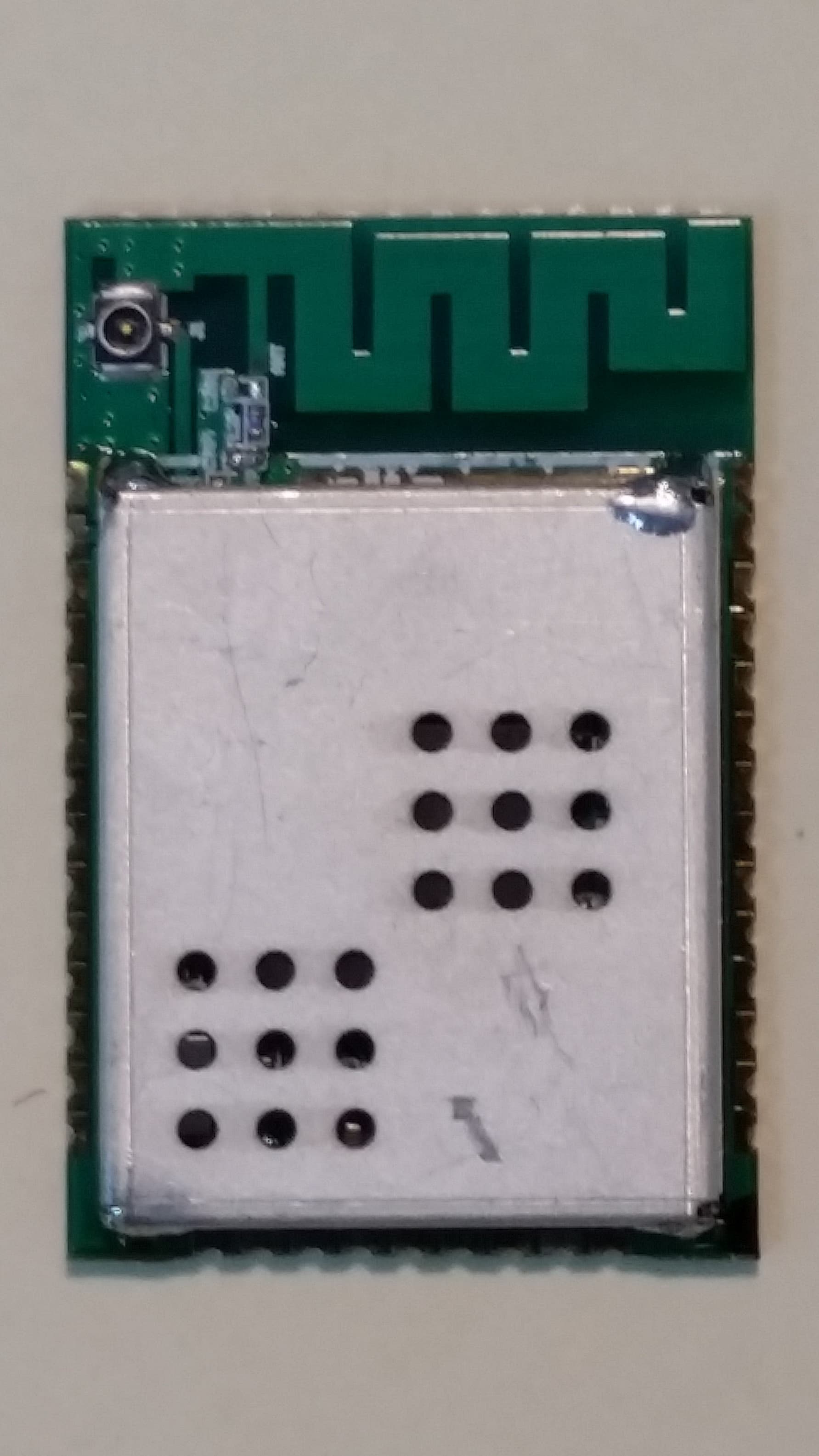
W7O24WN0
Aug 26, 2015802.11BGN 1X1 MODULE
Equipment Class
DTS - Digital Transmission System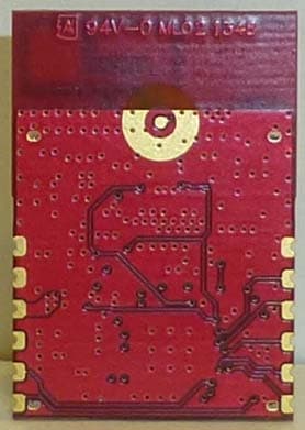
W7OMRF24J40MDME
Mar 05, 2014IEEE 802.15.4 RF Transceiver Module
Equipment Class
DTS - Digital Transmission System