WAP-CY5671CY5671 PRoC BLE Module
Cypress Semiconductor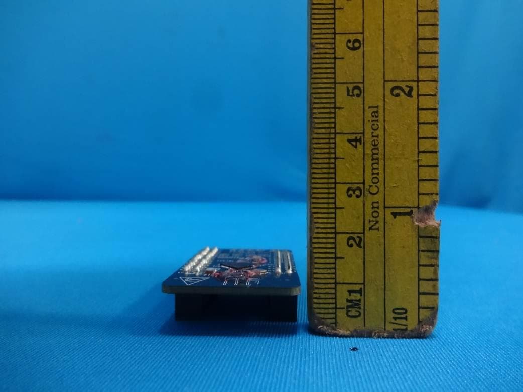
Click to zoom
Application Details
- Equipment Class
- DTS - Digital Transmission System
- Date of Grant
- Dec 31, 2014
- Application Purpose
- Original Equipment
- Date of Application
- Dec 21, 2014
- Equipment Note
- CY5671 PRoC BLE Module
- Frequency Range
- 2402.00000000 - 2480.00000000
- Company
- Cypress Semiconductor
- Country
- United States
Documents & Files
Document Text
Text extracted from the exhibit documents filed with the FCC. Open a document above to read the original.
Users Manual
CY8CKIT-042-BLE Bluetooth ® Low Energy (BLE) Pioneer Kit Guide Doc. # 001-93731 Rev. *A Cypress Semiconductor 198 Champion Court San Jose, CA 95134-1709 Phone (USA): 800.858.1810 Phone (Intnl): +1.408.943.2600 www.cypress.com CY8CKIT-042-BLE Bluetooth® Low Energy (BLE) Pioneer Kit Guide, Doc. # 001-93731 Rev. *A2 Copyrights © Cypress Semiconductor Corporation, 2014. The information contained herein is subject to change without notice. Cypress Semiconductor Corporation assumes no responsibility for the use of any circuitry other than circuitry embodied in a Cypress product. Nor does it convey or imply any license under patent or other rights. Cypress products are not warranted nor intended to be used for medical, life support, life saving, critical control or safety applications, unless pursuant to an express written agreement with Cypress. Furthermore, Cypress does not authorize its products for use as critical components in life- support systems where a malfunction or failure may reasonably be expected to result in significant injury to the user. The inclusion of Cypress products in life-support systems application implies that the manufacturer assumes all risk of such use and in doing so indemnifies Cypress against all charges. Any Source Code (software and/or firmware) is owned by Cypress Semiconductor Corporation (Cypress) and is protected by and subject to worldwide patent protection (United States and foreign), United States copyright laws and international treaty provisions. Cypress hereby grants to licensee a personal, non-exclusive, non-transferable license to copy, use, modify, create derivative works of, and compile the Cypress Source Code and derivative works for the sole purpose of creating custom software and or firmware in support of licensee product to be used only in conjunction with a Cypress integrated circuit as specified in the applicable agreement. Any reproduction, modification, translation, compilation, or representation of this Source Code except as specified above is prohibited without the express written permission of Cypress. Disclaimer: CYPRESS MAKES NO WARRANTY OF ANY KIND, EXPRESS OR IMPLIED, WITH REGARD TO THIS MATERIAL, INCLUDING, BUT NOT LIMITED TO, THE IMPLIED WARRANTIES OF MERCHANTABILITY AND FITNESS FOR A PARTICULAR PURPOSE. Cypress reserves the right to make changes without further notice to the materials described herein. Cypress does not assume any liability arising out of the application or use of any product or circuit described herein. Cypress does not authorize its products for use as critical components in life-support systems where a malfunction or failure may reasonably be expected to result in significant injury to the user. The inclusion of Cypress’ product in a life-support systems application implies that the manufacturer assumes all risk of such use and in doing so indemnifies Cypress against all charges. Use may be limited by and subject to the applicable Cypress software license agreement. CySmart, F-RAM, PRoC, Programmable System-on-Chip, and PSoC Creator are trademarks, and PSoC and CapSense are registered trademarks of Cypress Semiconductor Corporation. All other products and company names mentioned in this document may be the trademarks of their respective holders. Purchase of I 2 C components from Cypress or one of its sublicensed Associated Companies conveys a license under the Philips I 2 C Patent Rights to use these components in an I 2 C system, provided that the system conforms to the I 2 C Standard Specification as defined by Philips. As from October 1st, 2006 Philips Semiconductors has a new trade name - NXP Semiconductors. Flash Code Protection Cypress products meet the specifications contained in their particular Cypress Datasheets. Cypress believes that its family of products is one of the most secure families of its kind on the market today, regardless of how they are used. There may be methods, unknown to Cypress, that can breach the code protection features. Any of these methods, to our knowledge, would be dishonest and possibly illegal. Neither Cypress nor any other semiconductor manufacturer can guarantee the security of their code. Code protection does not mean that we are guaranteeing the product as “unbreakable.” Cypress is willing to work with the customer who is concerned about the integrity of their code. Code protection is constantly evolving. We at Cypress are committed to continuously improving the code protection features of our products. CY8CKIT-042-BLE Bluetooth® Low Energy (BLE) Pioneer Kit Guide, Doc. # 001-93731 Rev. *A3 Contents Safety Information 6 1. Introduction11 1.1Kit Contents ...............................................................................................................11 1.2Board Details .............................................................................................................12 1.3PSoC Creator™ .........................................................................................................15 1.4Getting Started...........................................................................................................16 1.5Additional Learning Resources ..................................................................................16 1.5.1 Beginner Resources.......................................................................................16 1.5.2 Application Notes ...........................................................................................16 1.5.3 PSoC Creator Example Projects ....................................................................17 1.5.4 Component Datasheets .................................................................................17 1.5.5 Bluetooth Learning Resources .......................................................................17 1.5.6 Learning From Peers .....................................................................................17 1.5.7 Other Related Resources..........................…
Text truncated - open the document above for the full version.
Users Manual
CY8CKIT-042-BLE Bluetooth® Low Energy (BLE) Pioneer Kit Guide, Doc. # 001-93731 Rev. *A106 Hardware 5.2BLE Module Board 5.2.1PSoC 4 BLE or PRoC BLE The PRoC BLE or PSoC 4 BLE is the main component on the BLE Module. It provides the RF interface and analog and digital capability. The PRoC BLE or PSoC 4 BLE pins are mapped to the Bluetooth module headers (see Figure 5-20). For more information, refer to the BLE web page. Figure 5-20. Schematics and Board Highlight of Bluetooth Module Headers for BLE Pins No Load al Pins PCA: 121-60159-01 PCB: 600-60195-01 P6.0 P6.1 /XRES P4.0 P4.1 P5.0 P5.1 XTAL24IXTAL24O P2.6P2.7P3.0P3.1P3.2P3.3P3.4P3.5P3.6P3.7 P1.6 P1.5 P1.4 P1.3 P1.2 P1.1 P2.4 P2.3 P2.2 P2.1 P2.0 P1.7 P2.5 P0.5 P0.3 P0.1 P1.0 P1.2 P0.0P0.1P0.2P0.3P0.4P0.5P0.6P0.7P1.0 VCCD VDDD VDDR VDDAVREF VDDA VDDD C13 1.2 pF ER 10x2 12 14 16 18 20 L1 6.8nH CY8C4247LQI-BL483 U1 VDDD 1 XTAL32O/P6.0 2 XTAL32I/P6.1 3 XRES 4 P4.0 5 P4.1 6 P5.0 7 P5.1 8 VSSD 9 VDDR 10 GANT1 11 ANT 12 GANT2 13 VDDR 14 P2.5 42 P2.4 41 P2.3 40 P2.2 39 P2.1 38 P2.0 37 VDDA 36 P1.7 35 P1.6 34 P1.5 33 P1.4 32 P1.3 31 P1.2 30 P1.1 29 EPAD 57 VCCD 56 VSSA 55 P3.7 54 P3.6 53 P3.5 52 P3.4 51 P3.3 50 P3.2 49 P3.1 48 P3.0 47 VDDA 46 VREF 45 P2.7 44 P2.6 43 VDDR 15 XTAL24I 16 XTAL24O 17 VDDR 18 P1.0 28 P0.0 19 P0.1 20 P0.2 21 P0.3 22 VDDD 23 P0.4 24 P0.5 25 P0.6 26 P0.7 27 J4 50 Ohm Wiggle Antenna 1122 C14 1.5 pF CY8CKIT-042-BLE Bluetooth® Low Energy (BLE) Pioneer Kit Guide, Doc. # 001-93731 Rev. *A107 Hardware 5.2.2Bluetooth Module Headers (20-Pin and 24-Pin Headers) The PSoC 4 BLE and PRoC BLE Modules connect to the Pioneer board using the two (20-pin and 24-pin) Bluetooth module headers (Figure 5-21). All GPIOs and power domains are brought out to these headers. These headers are the counterparts of the connectors in section 5.1.4. Figure 5-21. Schematics and Board Highlight of Headers Analog Pins Digital Pins P3.7P3.6 P3.5P3.4 P3.3P3.2 P3.1P3.0 P5.1P4.0 P5.0P4.1 P2.7P2.6 P2.5P2.4 P2.3P2.2 P2.1P2.0 P1.7 P1.5 P1.3 P0.5 P0.3 P0.1 P0.4 P0.2 P0.0 P1.6 /XRES P1.0 P1.1P1.2 P1.4 P0.7 P0.6 VDDA VDDR VDDD VREF J2 HEADER 10x2 12 34 56 78 910 1112 1314 1516 1718 1920 TP2 RED TP1 RED TP5 BLACK TP3 RED TP4 RED J1 HEADER 12x2 12 34 56 78 910 1112 1314 1516 1718 1920 2122 2324 CY8CKIT-042-BLE Bluetooth® Low Energy (BLE) Pioneer Kit Guide, Doc. # 001-93731 Rev. *A108 Hardware 5.2.3Wiggle Antenna Both the modules use the wiggle antenna. Refer to the Antenna Design Guide (AN91445) for details. Figure 5-22. Board Highlight of Wiggle Antenna CY8CKIT-042-BLE Bluetooth® Low Energy (BLE) Pioneer Kit Guide, Doc. # 001-93731 Rev. *A109 Hardware 5.2.4Antenna Matching Network An Antenna Matching Network is required between the BLE device and the antenna to achieve opti- mum performance (Figure 5-23). The matching network has four main tasks: ■Transform the balanced output of the radio to an unbalanced connection to the antenna (balun). ■Transform the output impedance of the radio to a 50-ohm antenna. ■Suppress harmonics to a level below the regulations level in TX mode. ■Suppress the local oscillator (LO) leakage in RX mode. Figure 5-23. Schematics and Board Highlight of Antenna Matching Network and Antenna CY8CKIT-042-BLE Bluetooth® Low Energy (BLE) Pioneer Kit Guide, Doc. # 001-93731 Rev. *A110 Hardware 5.2.5BLE Passives Module boards include a 24-MHz crystal and a 32-kHz crystal, the CMOD and shield (CTANK) circuit for CapSense, a SAR bypass capacitor, and adequate decoupling capacitors for all the power domains, as shown in Figure 5-24. Figure 5-24. Schematics and Board Highlight of External Crystal, CMOD, CTANK, Decaps, Jumpers SAR bypass CMOD Shunt Resistor C_Tank No Load No Load P4.0P4.1 VDDD VDDA VDDR VREF VCCDVDDD 0603 C20 1.0 uF 0402 C9 0.1 uF 0603 C10 1.0 uF 0603 C2 1.0 uF 0402 C1 0.1 uF C22 10000 pF 0603 C6 1.0 uF 0603 C17 1.0 uF 0603 C4 1.0 uF 0402 C5 0.1 uF 0402 C16 0.1 uF 0402 C3 0.1 uF 0603 C8 1.0 uF C21 2200 pF 0603 C19 1.0 uF 0603 C15 1.0 uF 0402 C18 0.1 uF 0805 R1 Zero Ohm 0805 R2 Zero Ohm 0603 C12 1.0 uF 0402 C11 0.1 uF 0402 C7 0.1 uF CY8CKIT-042-BLE Bluetooth® Low Energy (BLE) Pioneer Kit Guide, Doc. # 001-93731 Rev. *A111 Hardware 5.2.6Test Points All power domains are brought out as test points for easy probing. 5.3BLE Dongle Board See PSoC 4 BLE or PRoC BLE on page 106. See Wiggle Antenna on page 108. See Antenna Matching Network on page 109. See Pioneer Board LEDs on page 101. See Push Buttons on page 102. Figure 5-25. Board Highlight CY8CKIT-042-BLE Bluetooth® Low Energy (BLE) Pioneer Kit Guide, Doc. # 001-93731 Rev. *A112 Hardware 5.3.1Power System The board is powered directly using 5 V from the USB port, as shown in Figure 5-26. Figure 5-26. Power Supply Block Diagram With Protection Circuits 5.3.1.1Protection Circuits The PTC resettable fuse is connected to protect the computer's USB ports from shorts and overcur- rent. USB USB 5V PTC ESD P rotection PRoC PSoC5LP 5V 5V Headers CY8CKIT-042-BLE Bluetooth® Low Energy (BLE) Pioneer Kit Guide, Doc. # 001-93731 Rev. *A113 Hardware 5.3.2USB Type A Plug The PSoC 5LP connects to the USB port of a PC through a USB type A plug (Figure 5-27). This plug can also be used to power the board. A resettable polyfuse is used to protect the computer's USB ports from shorts and overcurrent. If more than 500 mA is applied to the USB port, the fuse will auto- matically break the connection until the short or overload is removed. The VBUS, D+, and D– lines from the USB connector are also protected against ESD events using TVS diodes. Figure 5-27. Schematics and Board Highlight of USB Type A Plug CY8CKIT-042-BLE Bluetooth® Low Energy (BLE) Pioneer Kit Guide, Doc. # 001-93731 Rev. *A114 Hardware 5.3.3User LED A user LED is provided to indicate status from the PRoC BLE device (Figure 5-28). It is also used to show the bind status. Figure 5-28. Schematics and Board Highlight of User LED BLE_STATUS 0805 R7 820 ohm 0805 LED1 Status LED Blue 21 CY8CKIT-042-BLE Bluetooth® Low Energy (BLE) Pioneer Kit Guide, Doc…
Text truncated - open the document above for the full version.
Block Diagram
www.tuv.com Appendix 5 Prüfbericht - Nr.: Test Report No. 19660133 001 Seite 1 von 1 Page 1 of 1 FCC ID : WAP-CY5671
Cover Letter(s)
Applicant/Grantee Cypress semiconductor/ WAP FCC ID: WAP-CY5671 Section 15.212 Modular Transmitters Request for Modular Approval Request for Limited Modular Approval Sl No Requirements EUT Conditions Comply (Y/N) 1 The radio elements of the modular Transmitter must have their own shielding. The physical crystal and tuning capacitors may be located external to the shielded radio elements. RF module meets the emission requirements of the FCC Part 15 without shielding N 2 The modular transmitter must have Buffered modulation/data inputs (if such inputs are provided) to ensure that the module will comply with Part 15 requirements under conditions of excessive data rates or over- modulation. Radio IC has internal buffers Y 3 The modular transmitter must have its Own power supply regulation. IC contains internal voltage regulator Y 4 The modular transmitter must comply with the antenna and transmission system requirements of Sections 15.203, 15.204(b) and 15.204(c). The antenna must either be permanently attached or employ a “unique” antenna coupler (at all connections between the module and the antenna, including the cable). The “professional installation” provision of Section 15.203 is not applicable to modules but can apply to limited modular approvals under paragraph (b) of this section. Yes the antenna is permanently attached. Y 5 The modular transmitter must be tested In a stand-alone configuration, i.e., the module must not be inside another device during testing for compliance with Part 15 requirements. Unless the transmitter module will be battery powered, it must comply with the AC line conducted requirements found in Section 15.207. AC or DC power lines and data input/output lines connected to the module must not contain ferrites; unless they will be marketed with the module (see Section 15.27(a)). The length of these lines shall be the length typical of actual use or, if that length is Module is tested with baseboard Y unknown, at least 10 centimeters to Insure that there is no coupling between the case of the module and supporting equipment. Any accessories, peripherals, or support equipment connected to the module during testing shall be unmodified and commercially available (see Section 15.31(i)). 6 The modular transmitter must be Equipped with either a permanently affixed label or must be capable of electronically displaying its FCC identification number. (A) If using a permanently affixed label, the modular transmitter must be labeled with its own FCC identification number, and, if the FCC identification number is not visible when the module is installed inside another device, then the outside of the device into which the module is installed must also display a label referring to the enclosed module. This exterior label can use wording such as the following: “Contains Transmitter Module FCC ID: XYZMODEL1” or “Contains FCC ID: XYZMODEL1.” Any similar wording that expresses the same meaning may be used. The Grantee may either provide such a label, an example of which must be included in the application for equipment Authorization, or, must provide adequate instructions along with the module which explain this requirement. In the latter case, a copy of these instructions must be included in the application for equipment authorization. (B) If the modular transmitter uses an electronic display of the FCC identification number, the Information must be readily accessible and visible on the modular transmitter or on the device in which it is installed. If the module is installed inside another device, then the outside of the device into which the module is installed must display a label referring to the enclosed module. This exterior label can use wording such as the following: “Contains FCC certified transmitter module(s).” Any similar wording that expresses the same meaning may be used. The user manual must No, Label is provided in the external packaging and on user manual due to space constrain. Y 7 The modular transmitter must comply With any specific rules or operating requirements that ordinarily apply to a complete transmitter and the manufacturer must provide adequate instructions along with the module to explain any such requirements. A copy This is detailed in the user manual. Y of these instructions must be included in The application for equipment authorization. 8 The modular transmitter must comply With any applicable RF exposure requirements in its final configuration. Yes, tested on its final configuration with baseboard. Y A limited modular approval may be granted for single or split modular transmitters that do not comply with all of the above requirements, e.g., shielding, minimum signaling amplitude, buffered modulation/data inputs, or power supply regulation, if the manufacturer can demonstrate by alternative means in the application for equipment authorization that the modular transmitter meets all the applicable Part 15 requirements under the operating conditions in which the transmitter will be used. Limited modular approval also may be granted in those instances where compliance with RF exposure rules is demonstrated only for particular product configurations. The applicant for certification must state how control of the end product into which the module will be installed will be maintained such that full compliance of the end product is always ensured. Best Regards, Signature Name/Title: Rinku Mathew/ Systems Engineer Staff Company Name: Cypress Semiconductor Date: 10-Dec-14
Cover Letter(s)
Cypress Semiconductor 198 Champion Court San Jose CA 95134 800-541-4736 / 408-943-2600 Date: 11/25/2014 Authorization letter for equipment authorization before FCC and or IC Canada, Re: FCC ID: WAP-CY8CKIT-142, WAP-CY5671 IC: 7922A-CY8CKIT142, 7922A-CY5671 To whom it may concern: Please be advised that Cypress Semiconductor Corporation, authorizes Rinku P Mathew of Cypress Semiconductors India Private Limited, to act on our behalf on all matters relating to application for equipment authorization before the federal communication Commission and Industry Canada, including signing of documents related to these matters. Cypress Semiconductor Corporation, Certifies that neither the applicant nor any party to this application, as defined in 47CFR Ch.1.2002 (b), is subjected to denial to federal benefits that includes FCC benefits, pursuant to section 5301 of anti-drug abuse act of 1998, 21 U.S.C.835 (a). Sincerely Brian Booker Applications Director Cypress Semiconductor Corporation Phone: 425-787-4469 Email: [email protected]
External Photos
www.tuv.com Appendix 2 Prüfbericht - Nr.: Test Report No. 19660134 001 Seite 1 von 2 Page 1 of 2 EUT Top View EUT Bottom View www.tuv.com Appendix 2 Prüfbericht - Nr.: Test Report No. 19660134 001 Seite 2 von 2 Page 2 of 2 EUT dimensional View EUT dimensional View
ID Label/Location Info
Label and Label Location
Internal Photos
www.tuv.com Appendix 2 Prüfbericht - Nr.: Test Report No. 19660134 001 Seite 1 von 2 Page 1 of 2 EUT Top View EUT Bottom View www.tuv.com Appendix 2 Prüfbericht - Nr.: Test Report No. 19660134 001 Seite 2 von 2 Page 2 of 2 EUT dimensional View EUT dimensional View
Operational Description
Theory of Operation/Technical Description – FCC ID: WAP-CY5671 The EUT enables customers to evaluate and develop Bluetooth Low Energy projects using the PSoC 4 BLE and PRoC BLE devices/silicon. The basic operation mode is: • BLE communication was established between CY5670 CySmart USB Dongle and CY5671 PRoC BLE Module plugged into BLE Pioneer Baseboard. RF circuit function: This CY5671 PRoC BLE Module board act as a basic breakout board for the CYBL10563-56LQXI BLE silicon. In addition to including the PRoC BLE devices, the module boards also contain the BLE passives (resistors, capacitors, external crystals, and antenna-matching network), an on-board antenna, and headers for connecting to the baseboard. The baseboard contains the power supply section (USB and battery), an on-board programmer/debugger, a 1-Mb F-RAM, an RGB LED, a five-segment CapSense slider, a proximity header, a user switch, and a reset switch for interfacing with the module. RF signal flow: Description of Antenna system (Baluns, Multiplexers) The Modules/Dongle uses the wiggle antenna (PCB antenna; Meandered Inverted-F Antenna). Refer to the Antenna Design Guide (AN91445 attached) for details. Classification of specified radio equipment Class: 2.4GHz Low Power Data Communication – Bluetooth low energy Frequency: F1D 2402MHz~2480MHz (2MHz separation 40 channels) Modulation method: GFSK; Frequency Deviation +/-250 kHz, Data Speed 1Mbps Operation power/voltage: DC Max 5V Maximum power of the module: 0dBm; (Note: This power cannot be set higher than the 0dBm)
Operational Description
www.cypress.com Document No. 001-91445 Rev. ** 1 AN91445 Antenna Design Guide Author: Gowrish B. Associated Part Family: CY8C4XX7-BL, CYBL10X6X Related Application Notes: None To get the latest version of this application note and the associated Gerber file, please visit http://www.cypress.com/go/AN91445 AN91445 explains antenna design in simple terms and recommends two Cypress-tested PCB antennas that can be implemented at a very low cost for use with the Bluetooth Low Energy (BLE) solutions that are part of Cypress’s PRoC™ and PSoC ® family. The PRoC BLE and PSoC 4 BLE 2.4 GHz radio must be carefully matched to its antenna for optimum performance. It concludes by showing how to tune the antenna in the final product. Contents Introduction ....................................................................... 1 Antenna Parameters ......................................................... 2 Recommended PCB Antennas ......................................... 2 Meandered Inverted-F Antenna (MIFA) ........................ 3 Inverted-F Antenna (IFA) .............................................. 4 Chip Antennas ................................................................... 5 Antenna Comparison......................................................... 5 Selecting the PCB Antenna ............................................... 5 Antenna Tuning ................................................................. 6 Solution 1: Antenna Length Tuning .............................. 6 Solution 2: Antenna Matching Network ........................ 7 Solution 1 Versus Solution 2 ........................................ 8 Summary ........................................................................... 9 Appendix A: 7-Step Design ............................................. 10 Appendix B: Checklist ..................................................... 11 Appendix C: References ................................................. 12 Worldwide Sales and Design Support ............................. 14 Introduction The goal of this application note is to enable you to design an optimal antenna for your application with minimal time and resources. The antenna is a vital component in a wireless system. A well-designed antenna will help to optimize the performance of the PRoC BLE and PSoC 4 BLE radio in the final product. The antenna can be considered as an energy translator. It converts electrical energy into electromagnetic waves for transmission and reconverts the electromagnetic waves into electrical energy on reception. Figure 1 gives a holistic view of a typical wireless system. Figure 1. Typical Wireless System A well-designed antenna increases the operating range of the wireless product. The more power it can transmit from the radio, the larger the distance it can cover for a given packet error rate (PER). Other benefits are less obvious. For example, for a given range, a well-designed antenna radiates more power and thus has a higher margin for error (caused by interference or noise). This reduces the PER and improves the communication quality. The lower the PER (due to the higher margin for error), the fewer will be the retransmissions, thus saving battery energy. MN Matching Network Radio Transmission Line (50 ) Antenna PRoC BLE / PSoC 4 BLE Antenna Design Guide www.cypress.com Document No. 001-91445 Rev. ** 2 Therefore, an optimal antenna design is important for low- energy applications. It is generally believed that antenna design is difficult because the antenna is sensitive to PCB size, nearby plastic casing, and other factors, that can detune it. This application note gives a step-by-step antenna design procedure to optimize the radio performance of a PRoC BLE or PSoC 4 BLE design. Antenna Parameters Following are some key antenna performance parameters, with an emphasis on physical significance. Return loss: Return loss of an antenna signifies how well the antenna is matched to the 50 transmission line (TL). TL impedance is typically 50 , although it could be a different value. The industry standard for commercial antennas and testing equipment is 50- impedance, so it is most convenient to use this value. Return loss indicates how much of the incident power is reflected by the antenna due to mismatch (Equation 1). Ideally, the entire incident power is radiated without any reflection from the antenna. If the return loss is infinite, the antenna is said to be perfectly matched to the TL, as shown in Figure 2. S 11 is the negation of return loss expressed in decibels. As a rule of thumb, a return loss ≥ 10 dB (equivalently, S 11 ≤ –10 dB) is considered sufficient. Table 1 relates the return loss (dB) to the power reflected from the antenna (percent). Equation 1 Figure 2. Return Loss Table 1. Return Loss and Power Reflected From Antenna S 11 (dB) Return Loss (dB) P reflected / P incident (%) P radiated / P incident (%) –20 20 1 99 –10 10 10 90 –3 3 50 50 –1 1 79 21 Bandwidth: Bandwidth indicates the frequency response of an antenna. It signifies how well the antenna is matched to the 50- transmission line over the entire band of interest, that is, between 2.40 GHz and 2.48 GHz for BLE applications. Radiation efficiency: A portion of non-reflected power (Figure 2) gets dissipated as heat or as thermal loss in the antenna. Thermal loss is due to the dielectric loss in the FR4 substrate and the conductor loss in the copper trace. This information is characterized as radiation efficiency. A radiation efficiency of 100 percent indicates that all non-reflected power is radiated to air. Radiation pattern: Radiation pattern indicates the directional property of radiation, that is, which directions have more radiation and which have less. This information helps to orient the antenna properly. Gain: Gain gives information on radiation in the direction of interest, compared to the isotropic antenna, which radiates uniformly in all directions spherically. An analogy for the isotropic antenna is…
Text truncated - open the document above for the full version.
RF Exposure Info
www.tuv.com Appendix 4 Prüfbericht - Nr.: Test Report No. 19660133 001 Seite 1 von 1 Page 1 of 1 RF Exposure Report RESULT: Passed Test standard : FCC KDB Publication 447498 Since maximum peak output power of the transmitter at 2402MHz is 1.15318 mW < 10 mW, hence the EUT is excluded from SAR evaluation according to FCC KDB publication 447498 D01 v05: Mobile Portable RF Exposure.
Schematics
55 44 33 22 11 D D C C B B A A SAR bypass CMOD Shunt Resistor C_Tank KHz Crystal MHz Crystal TXRX Analog Pins Serial Interface No Load No Load No Load No Load No Load Digital Pins No Load No Load No Load No Load No Load No Load PCA: 121-60160-01PCB: 600-60196-01FAB DRW: 610-60188-01ASSY DRW: 620-60196-01 P4.0 P4.1 P6.0P6.1 XTAL24OXTAL24I P6.0P6.1/XRESP4.0P4.1P5.0P5.1 XTAL24I XTAL24O P2.6 P2.7 P3.0 P3.1 P3.2 P3.3 P3.4 P3.5 P3.6 P3.7 P1.5P1.4 /XRES P1.6P1.5P1.4P1.3P1.2P1.1P2.4P2.3P2.2P2.1P2.0P1.7P2.5 P3.7 P3.6 P3.5 P3.4 P3.3 P3.2 P3.1 P3.0 P5.1 P4.0 P5.0 P4.1 P2.7 P2.6 P2.5 P2.4 P2.3 P2.2 P2.1 P2.0P1.7P1.5P1.3 P0.5P0.3P0.1 P0.4P0.2P0.0P1.6 /XRESP1.0 P1.1 P1.2 P1.4 P0.7P0.6 P0.0 P0.1 P0.2 P0.3 P0.4 P0.5 P0.6 P0.7 P1.0 VDDDVDDAVDDR VCCD VDDD VREF VDDR VDDA VREF VDDR VDDD VDDA VDDD VCCD VDDD VDDA VDDA VDDR VDDD VREF VDDD TitleSize Document Number R e v Date: Sheet o f CYPRESS SEMICONDUCTOR © 2014 04 CY5671 PRoC BLE Module A4 Tuesday, September 30, 2014 630-60192-01 Title Size Document Number R e v Date: Sheet o f CYPRESS SEMICONDUCTOR © 2014 04 CY5671 PRoC BLE Module A4 Tuesday, September 30, 2014 630-60192-01 Title Size Document Number R e v Date: Sheet o f CYPRESS SEMICONDUCTOR © 2014 04 CY5671 PRoC BLE Module A4 1 1 Tuesday, September 30, 2014 630-60192-01 0603 C101.0 uF 0402 C9 0.1 uF C13 1.2 pF 0603 C201.0 uF J2 HEADER 10x2 1 2 3 4 5 6 7 8 9 10 11 12 13 14 15 16 17 18 19 20 0603 C21.0 uF L4 330 OHM @ 100MHz 0402 C1 0.1 uF TP2RED C2336 pF C22 10000 pF 0603 C25100 pF 0603 C41.0 uF 0603 C171.0 uF 0603 C61.0 uF 0402 C3 0.1 uF 0402 C16 0.1 uF 0402 C5 0.1 uF C212200 pF L3 330 OHM @ 100MHz TP1RED 0603 C81.0 uF 0603 C191.0 uF R1 Zero Ohm 0402 C18 0.1 uF 0603 C151.0 uF J3 4 HEADER 1234 R2 Zero Ohm L1 6.8nH 0603 C121.0 uF C2418 pF TP3RED 0402 C11 0.1 uF Y1 32.768KHz 12 TP5BLACK CYBL10563-56LQXI U1 VDDD 1 XTAL32O/P6.0 2 XTAL32I/P6.1 3 XRES 4 P4.0 5 P4.1 6 P5.0 7 P5.1 8 VSSD 9 VDDR 10 GANT1 11 ANT 12 GANT2 13 VDDR 14 P2.5 42 P2.4 41 P2.3 40 P2.2 39 P2.1 38 P2.0 37 VDDA 36 P1.7 35 P1.6 34 P1.5 33 P1.4 32 P1.3 31 P1.2 30 P1.1 29 EPAD 57 VCCD 56 VSSA 55 P3.7 54 P3.6 53 P3.5 52 P3.4 51 P3.3 50 P3.2 49 P3.1 48 P3.0 47 VDDA 46 VREF 45 P2.7 44 P2.6 43 VDDR 15 XTAL24I 16 XTAL24O 17 VDDR 18 P1.0 28 P0.0 19 P0.1 20 P0.2 21 P0.3 22 VDDD 23 P0.4 24 P0.5 25 P0.6 26 P0.7 27 Y224Mhz 1 2 3 4 TP4 RED R3 4.7K L2 330 OHM @ 100MHz J1 HEADER 12x2 1 2 3 4 5 6 7 8 9 10 11 12 13 14 15 16 17 18 19 20 21 22 23 24 J4 50 Ohm Wiggle Antenna 11 22 C141.5 pF 0402 C7 0.1 uF
Test Report
www.tuv.com Test Report No.: 19660133 001 Date: 19.03.2014 Page 2 of 25 Test Result Summary Clause Test Item Result FCC 15.247(b) (3) Maximum Conducted Peak Output Power Pass FCC 15.247(a) (2) DTS (6dB) Bandwidth Pass FCC 15.247(e) Power Spectral Density Pass FCC 15.247(d) Band-edge compliance Pass FCC 15.209 / FCC 15.205 Spurious Radiated Emissions and Restricted Bands of Operation Pa…
Text truncated - open the document above for the full version.
Contact Information
Applicant
Juan Martinez(Senor System Engineer)
Test Firm
TUV Rheinland (India) Pvt. Ltd.,B GURUPRASAD
Technical Specifications
| # | Rule Parts | Frequency Range | Power Output |
|---|---|---|---|
| 1 | 15C | 2.40 GHz - 2.48 GHz | 1.15 mW |
Other Applications from Cypress Semiconductor
WAP829I20
Aug 04, 2024AIROC Bluetooth LE Module
Equipment Class
DTS - Digital Transmission System
WAP739I05
Aug 01, 2024AIROC Matter Module
Equipment Class
DTS - Digital Transmission SystemWAP829I10
Jan 16, 2024AIROC Bluetooth LE Module
Equipment Class
DTS - Digital Transmission System
WAP3068
Jun 28, 2020EZ-BT WICED Module
Equipment Class
DTS - Digital Transmission System
WAP3066
Jun 23, 2020EZ-BT WICED Module
Equipment Class
DSS - Part 15 Spread Spectrum Transmitter