WAP3063EZ-BT WICED Module
Cypress Semiconductor
Click to zoom
Application Details
- Equipment Class
- DTS - Digital Transmission System
- Date of Grant
- Jan 14, 2020
- Application Purpose
- Original Equipment
- Date of Application
- Jan 14, 2020
- Equipment Note
- EZ-BT WICED Module
- Frequency Range
- 2402.00000000 - 2480.00000000
- Company
- Cypress Semiconductor
- Country
- United States
Documents & Files
Document Text
Text extracted from the exhibit documents filed with the FCC. Open a document above to read the original.
Users Manual
PRELIMINARY CYBT-273063-02 CYBT-263064-02 CYBT-263065-02 EZ-BT™ Module Cypress Semiconductor Corporation• 198 Champion Court• San Jose,CA 95134-1709 • 408-943-2600 Document Number: 002-29354 Rev. ** Revised December 26, 2019 CYBT-273063-02, CYBT-263064-02, CYBT-263065-02, EZ-BT™ Module General Description The CYBT-2X30XX-02 is a dual-mode Bluetooth BR/EDR and Low Energy (BLE) wireless module solution. The CYBT-2X30XX-02 includes an onboard crystal oscillator, passive components, PA/LNA, and the Cypress CYW20819 silicon device. The CYBT-2X30XX-02 supports a number of peripheral functions (ADC, PWM), as well as multiple serial communication protocols (UART, SPI, I 2 C, I 2 S/PCM). The CYBT-2X30XX-02 includes a royalty-free stack compatible with Bluetooth 5.0 in a 12.0 × 16.61 × 1.70 mm module form-factor. The CYBT-2X30XX-02 is offered in three certified versions CYBT-273063-02, CYBT-263064-02, and CYBT-263065-02. The CYBT-273063-02 includes an integrated trace antenna. The CYBT-263064-02 supports an external antenna via a u-FL connector. The CYBT-263065-02 supports an external antenna through a RF solder pad output. CYBT-2X30XX-02 includes onboard external power/low noise amplifier, qualified by Bluetooth SIG, and includes regulatory certification approval for FCC, ISED, MIC, and CE. Module Description ■Module size: 12.5 mm × 19 mm × 1.95 mm ■Complies with Bluetooth Core Specification version 5.0 and includes support for BR, EDR 2/3 Mbps, eSCO, BLE, LE 2 Mbps, as well as Bluetooth Mesh. ❐QDID: TBD ❐Declaration ID: TBD ■Certified to FCC, ISED, MIC, and CE standards ■256-KB on-chip Flash, 176-KB on-chip RAM ■Industrial temperature range: –30 °C to +85 °C ■Integrated Arm ® Cortex ® -M4 microprocessor core with floating point unit (FPU) RF Characteristics ■Maximum TX output power: +17.0 dBm ■BLE RX Receive Sensitivity: –95.0 dBm Power Consumption ■TX current consumption ❐BLE silicon: 5.8 mA (radio only, 4 dBm) ❐8TR8201: 8 mA Typ (PA/LNA only) ■RX current consumption ❐Bluetooth silicon: 5.9 mA (radio only) ❐8TR8201: 75 mA Typ (PA/LNA only, +20 dBm Pout) ❐8TR8201: ?? mA Typ (PA/LNA only, +7.5 dBm Pout) ■Cypress CYW20819 silicon low power mode support ❐PDS: 16.5 μA with 176 KB RAM retention ❐ePDS: 8.7 μA ❐HIDOFF (wake on external or timed interrupt): 1.75 μA Functional Capabilities ■Up to 20 GPIOs ■I 2 C, I2S, UART, and PCM interfaces ■Two Quad-SPI interfaces ■Auxiliary ADC with up to 15 analog channels ■Programmable key scan 20 × 8 matrix ■General-purpose timers and six PWMs ■Real-time clock (RTC) and watchdog timers (WDT) ■Bluetooth Basic Rate (BR) and Enhanced Data Rate (EDR) Support ■BLE protocol stack supporting generic access profile (GAP) Central, Peripheral, Observer, or Broadcaster roles Benefits CYBT-2X30XX-02 is fully integrated and certified solution that provides all necessary components required to operate Bluetooth communication standards. ■Proven hardware design ready to use ■Ultra-flexible supermux I/O design allows maximum flexibility for GPIO function assignment ■Over-the-air update capable for development or field updates ■Bluetooth SIG qualified. ■ModusToolbox™ provides an easy-to-use integrated design environment (IDE) to configure, develop, program, and test your Bluetooth application Document Number: 002-29354 Rev. ** Page 2 of 45 PRELIMINARY CYBT-273063-02 CYBT-263064-02 CYBT-263065-02 More Information Cypress provides a wealth of data at www.cypress.com to help you to select the right module for your design, and to help you to quickly and effectively integrate the module into your design. References ■Overview: EZ-BLE/EZ-BT Module Portfolio, Module Roadmap ■Development Kits: ❐CYBT-273063-EVAL, CYBT-273063-02 Evaluation Board ❐CYBT-263064-EVAL, CYBT-263064-02 Evaluation Board ❐CYBT-213043-MESH, Mesh Evaluation Kit ❐CYW920819Q40EVB-01, Evaluation Kit for CYW20819 silicon device ■Test and Debug Tools: ❐CYSmart, Bluetooth ® LE Test and Debug Tool (Windows) ❐CYSmart Mobile, Bluetooth ® LE Test and Debug Tool (Android/iOS Mobile App) ■Knowledge Base Article ❐KBA97095 - EZ-BLE™ Module Placement ❐RF Regulatory Certifications for CYBT-2X30XX-02 EZ-BT WICED Modules (TBD) ❐KBA213976 - FAQ for BLE and Regulatory Certifications with EZ-BLE modules ❐KBA210802 - Queries on BLE Qualification and Declaration Processes ❐KBA218122 - 3D Model Files for EZ-BLE/EZ-BT Modules ❐KBA223428 - Programming an EZ-BT WICED Module ❐KBA225450 - Putting 2073x, 2070x, and 20719 Based De- vices or Modules in HCI Mode Development Environments ModusToolbox Integrated Development Environment (IDE) ModusToolbox simplifies development for IoT designers. It delivers easy-to-use tools and a familiar microcontroller (MCU) integrated development environment (IDE) for Windows ® , macOS ® , and Linux ® . It provides a sophisticated environment for system setup, wireless connectivity libraries, power analysis, application-specific configurators for Bluetooth ® Low Energy (BLE), CapSense ® , as well as other peripherals. In addition, code examples, documentation, technical support and community forums are available to help your IoT development process along. These tools and features enable an IoT designer to develop innovative IoT applications efficiently and with ease. Technical Support ■Cypress Community: Whether you are a customer, partner, or a developer interested in the latest Cypress innovations, the Cypress Developer Community offers you a place to learn, share, and engage with both Cypress experts and other embedded engineers around the world. ■Frequently Asked Questions (FAQs): Learn more about our Bluetooth ecosystem. ■Visit our support page and create a technical support case or contact a local sales representatives. If you are in the United States, you can talk to our technical support team by calling our toll-free number: +1-800-541-4736. Select option 2 at the prompt. Document Number: 002-29354 Rev. ** Page 3 of 45 PRELIMINARY CYBT-273063-02 CYBT-263064-02 CYBT-263065-02 Contents Overview ..............…
Text truncated - open the document above for the full version.
Cover Letter(s)
Cypress Semiconductor 198 Champion Court, San Jose, CA, USA, 95134 Date: 1/10/2020 Authorization letter for equipment authorization before FCC and/or IC Canada, Re: FCC ID: WAP3063 IC: 7922A-3063 To whom it may concern: Please be advised that Cypress Semiconductor Corporation authorizes Yedan LI of Cypress Semiconductor Technology (shanghai) co. ltd., to act on our behalf on all matters relating to application for equipment authorization before the federal communication Commission and Industry Canada, including signing of documents related to these matters. Cypress Semiconductor Corporation, Certifies that neither the applicant nor any party to this application, as defined in 47CFR Ch.1.2002 (b), is subjected to denial to federal benefits that includes FCC benefits, pursuant to section 5301 of anti-drug abuse act of 1998, 21 U.S.C.835 (a). Sincerely David Solda Cypress Semiconductor Corporation Phone: (408)943-2600 1639 Email: [email protected] Business Unit Vice President
Cover Letter(s)
Cypress Semiconductor Office of Engineering Technology Federal Communications Commission 7435 Oakland Mills Road Columbia, MD21046 Subject; Request for Long Term Confidentiality FCC ID: WAP3063 To Whom It May Concern, Pursuant to the provisions of the Commission’s rules Title 47 Sections §0.457 and §0.459, we are requesting the Commission to withhold the following attachment(s) as confidential documents from public disclosure indefinitely. These documents contain detailed system and equipment descriptions and are considered as proprietary information in operation of the equipment. The public disclosure of these documents might be harmful to our company and would give competitors an unfair advantage in the market. Schematic Diagram Block Diagram Parts List Operational Description Tune Up It is our understanding that all measurement test reports, FCC ID label format and correspondence during the certification review process cannot be granted as confidential documents and this information will be available for public review once the grant of equipment authorization is issued. Print name: Yedan LI Signed name: Date: January 10, 2020 Company: Cypress Semiconductor Address: 198 Champion Ct, San Jose, California 95134, United States
Cover Letter(s)
Cypress Semiconductor POWER OF ATTORNEY DATE: January 9, 2020 To: Federal Communications Commission, Authorization & Evaluation Division, 7435 Oakland Mills Road, Columbia, MD 21046 We, the undersigned, hereby authorize TA Technology (Shanghai) Co., Ltd. /Lu Rui on our behalf, to apply to FCC on our equipment for FCC ID: WAP3063. Any and all acts carried out by TA Technology (Shanghai) Co., Ltd. / Lu Rui on our behalf shall have the same effect as acts of our own. Sincerely, Signature: Print name: Yedan LI Company: Cypress Semiconductor
External Photos
External Photo Company: Cypress Semiconductor Model: CYBT-263065-02 CYBT-263064-02 CYBT-273063-02
ID Label/Location Info
Label Location Company: Cypress Semiconductor FCC ID: WAP3063 Label Location Company: Cypress Semiconductor FCC ID: WAP3063 Label Location Company: Cypress Semiconductor FCC ID: WAP3063
Internal Photos
Internal Photo Company: Cypress Semiconductor Model: CYBT-263065-02 CYBT-263064-02 CYBT-273063-02 Internal Photo Company: Cypress Semiconductor Model: CYBT-263065-02 CYBT-263064-02 CYBT-273063-02
RF Exposure Info
MPE TEST REPORT Applicant Cypress Semiconductor FCC ID WAP3063 Product EZ-BT WICED Module Model CYBT-273063-02 CYBT-263064-02 CYBT-263065-02 Report No. R1911A0639-M1 Issue Date January 3, 2020 TA Technology (Shanghai) Co., Ltd. tested the above equipment in accordance with the requirements in FCC 47 CFR Part 1 1.1310. The test results show that the equipment tested is capable of demonstrating compliance with the requirements as documented in this report. Performed by: Yu Wang Approved by: Guangchang Fan TA Technology (Shanghai) Co., Ltd. No.145, Jintang Rd, Tangzhen Industry Park, Pudong Shanghai, China TEL: +86-021-50791141/2/3 FAX: +86-021-50791141/2/3-8000 MPE Test Report Report No.: R1911A0639-M1 TA Technology (Shanghai) Co., Ltd. TA-MB-01-013S Page 2 of 9 This report shall not be reproduced except in full, without the written approval of TA Technology (Shanghai) Co., Ltd. Table of Contents 1 Test Laboratory ............................................................................................................................... 3 1.1 Notes of the Test Report ......................................................................................................... 3 1.2 Testing Location ...................................................................................................................... 3 1.3 Laboratory Environment .......................................................................................................... 4 2 Description of Equipment under Test .............................................................................................. 5 3 Maximum conducted output power (measured) and antenna Gain ................................................ 6 4 Test Result ..................................................................................................................................... 7 MPE Test Report Report No.: R1911A0639-M1 TA Technology (Shanghai) Co., Ltd. TA-MB-01-013S Page 3 of 9 This report shall not be reproduced except in full, without the written approval of TA Technology (Shanghai) Co., Ltd. 1 Test Laboratory 1.1 Notes of the Test Report This report shall not be reproduced in full or partial, without the written approval of TA technology (shanghai) co., Ltd.The results documented in this report apply only to the tested sample, under the conditions and modes of operation as described herein .Measurement Uncertainties were not taken into account and are published for informational purposes only. This report is written to support regulatory compliance of the applicable standards stated above. 1.2 Test facility FCC (Designation number: CN1179, Test Firm Registration Number: 446626) TA Technology (Shanghai) Co., Ltd. has been listed on the US Federal Communications Commission list of test facilities recognized to perform electromagnetic emissions measurements. A2LA (Certificate Number: 3857.01) TA Technology (Shanghai) Co., Ltd. has been listed by American Association for Laboratory Accreditation to perform electromagnetic emission measurement. 1.3 Testing Location Company: TA Technology (Shanghai) Co., Ltd. Address: No.145, Jintang Rd, Tangzhen Industry Park, Pudong Shanghai, China City: Shanghai Post code: 201201 Country: P. R. China Contact: Xu Kai Telephone: +86-021-50791141/2/3 Fax: +86-021-50791141/2/3-8000 Website: http://www.ta-shanghai.com E-mail: [email protected] MPE Test Report Report No.: R1911A0639-M1 TA Technology (Shanghai) Co., Ltd. TA-MB-01-013S Page 4 of 9 This report shall not be reproduced except in full, without the written approval of TA Technology (Shanghai) Co., Ltd. 1.4 Laboratory Environment Temperature Min. = 18C, Max. = 25 C Relative humidity Min. = 30%, Max. = 70% Ground system resistance < 0.5 Ambient noise is checked and found very low and in compliance with requirement of standards. Reflection of surrounding objects is minimized and in compliance with requirement of standards. MPE Test Report Report No.: R1911A0639-M1 TA Technology (Shanghai) Co., Ltd. TA-MB-01-013S Page 5 of 9 This report shall not be reproduced except in full, without the written approval of TA Technology (Shanghai) Co., Ltd. 2 Description of Equipment under Test Client Information Applicant Cypress Semiconductor Applicant address 198 Champion Ct, San Jose, California 95134,United States Manufacturer Cypress Semiconductor Manufacturer address 198 Champion Ct, San Jose, California 95134,United States General Technologies Model CYBT-273063-02 CYBT-263064-02 CYBT-263065-02 SN 1# Hardware Version REV1.0 Software Version REV1.0 Date of Testing: December 6, 2019 ~ December 20, 2019 Note: 1. The EUT is sent from the applicant to TA and the information of the EUT is declared by the applicant. 2. All indications of Pass/Fail in this report are opinions expressed by TA Technology (Shanghai) Co., Ltd. based on interpretations and/or observations of test results. Measurement Uncertainties were not taken into account and are published for informational purposes only. Difference Configuration Statement Model CYBT-273063-02CYBT-263064-02 CYBT-263065-02 The configuration of antenna PCB antenna External antenna via RF pin on the bottom of the module External dipole antenna via UFL connector Antenna gain 0.7dBi 2.0dBi 2.0dBi Others The same The same The same The difference between the two EUT is only the configuration of antenna and antenna gain. There are more than one Configure, each one should be applied throughout the compliance test respectively, however, the worst case (CYBT-263065-02) will be recorded for conducted items and the radiated items are recorded for all. MPE Test Report Report No.: R1911A0639-M1 TA Technology (Shanghai) Co., Ltd. TA-MB-01-013S Page 6 of 9 This report shall not be reproduced except in full, without the written approval of TA Technology (Shanghai) Co., Ltd. 3 Maximum conducted output power (measured) and antenna Gain The numeric gain (G) of the antenna with a gain specified in dB is determined by Numeric ga…
Text truncated - open the document above for the full version.
Test Report
RF TEST REPORT Applicant Cypress Semiconductor FCC ID WAP3063 Product EZ-BT WICED Module Model CYBT-273063-02 CYBT-263064-02 CYBT-263065-02 Report No. R1911A0639-R2 Issue Date January 3, 2020 TA Technology (Shanghai) Co., Ltd. tested the above equipment in accordance with the requirements in FCC CFR47 Part 15C (2018). The test results show that the equipment tested is capable of demonstrating compliance with the requirements as documented in this report. Performed by: Peng Tao Approved by: Kai Xu TA Technology (Shanghai) Co., Ltd. No.145, Jintang Rd, Tangzhen Industry Park, Pudong Shanghai, China TEL: +86‐021‐50791141/2/3 FAX: +86‐021‐50791141/2/3‐8000 RF Test Report Report No.: R1911A0639-R2 TA Technology (Shanghai) Co., Ltd. TA-MB-04-005R Page 2 of 39 This report shall not be reproduced except in full, without the written approval of TA Technology (Shanghai) Co., Ltd. TABLE OF CONTENT 1. Test Laboratory ............................................................................................................................ 4 1.1. Notes of the test report ......................................................................................................... 4 1.2. Testing Location ................................................................................................................... 4 2. General Description of Equipment under Test .............................................................................. 5 2.1. Applicant and Manufacturer Information ............................................................................... 5 2.2. General information .............................................................................................................. 5 3. Applied Standards ........................................................................................................................ 7 4. Test Configuration ........................................................................................................................ 8 5. Test Case Results ........................................................................................................................ 9 5.1. Maximum output power ........................................................................................................ 9 5.2. 6dB Bandwidth ................................................................................................................... 11 5.3. Band Edge ......................................................................................................................... 15 5.4. Power Spectral Density ...................................................................................................... 17 5.5. Spurious RF Conducted Emissions .................................................................................... 20 5.6. Unwanted Emission ........................................................................................................... 23 5.7. Conducted Emission .......................................................................................................... 36 6. Main Test Instruments ................................................................................................................ 39 RF Test Report Report No.: R1911A0639-R2 TA Technology (Shanghai) Co., Ltd. TA-MB-04-005R Page 3 of 39 This report shall not be reproduced except in full, without the written approval of TA Technology (Shanghai) Co., Ltd. Summary of measurement results Number Test Case Clause in FCC rules Verdict 1 Maximum conducted output power 15.247(b)(3) PASS 2 6 dB bandwidth 15.247(a)(2) PASS 3 Power spectral density 15.247(e) PASS 4 Band Edge 15.247(d) PASS 5 Spurious RF Conducted Emissions 15.247(d) PASS 6 Unwanted Emissions 15.247(d),15.205,15.209 PASS 7 Conducted Emissions 15.207 PASS Date of Testing: December 6, 2019 ~ December 20, 2019 Note: All indications of Pass/Fail in this report are opinions expressed by TA Technology (Shanghai) Co., Ltd. based on interpretations and/or observations of test results. Measurement Uncertainties were not taken into account and are published for informational purposes only. RF Test Report Report No.: R1911A0639-R2 TA Technology (Shanghai) Co., Ltd. TA-MB-04-005R Page 4 of 39 This report shall not be reproduced except in full, without the written approval of TA Technology (Shanghai) Co., Ltd. 1. Test Laboratory 1.1. Notes of the test report This report shall not be reproduced in full or partial, without the written approval of TA technology (shanghai) co., Ltd. The results documented in this report apply only to the tested sample, under the conditions and modes of operation as described herein .Measurement Uncertainties were not taken into account and are published for informational purposes only. This report is written to support regulatory compliance of the applicable standards stated above. 1.2. Test facility FCC (Designation number: CN1179, Test Firm Registration Number: 446626) TA Technology (Shanghai) Co., Ltd. has been listed on the US Federal Communications Commission list of test facilities recognized to perform electromagnetic emissions measurements. A2LA (Certificate Number: 3857.01) TA Technology (Shanghai) Co., Ltd. has been listed by American Association for Laboratory Accreditation to perform electromagnetic emission measurement. 1.3. Testing Location Company: TA Technology (Shanghai) Co., Ltd. Address: No.145, Jintang Rd, Tangzhen Industry Park, Pudong City: Shanghai Post code: 201201 Country: P. R. China Contact: Xu Kai Telephone: +86-021-50791141/2/3 Fax: +86-021-50791141/2/3-8000 Website: http://www.ta-shanghai.com E-mail: [email protected] RF Test Report Report No.: R1911A0639-R2 TA Technology (Shanghai) Co., Ltd. TA-MB-04-005R Page 5 of 39 This report shall not be reproduced except in full, without the written approval of TA Technology (Shanghai) Co., Ltd. 2. General Description of Equipment under Test 2.1. Applicant and Manufacturer Information Applicant Cypress Semicon…
Text truncated - open the document above for the full version.
Test Setup Photos
RF Test Setup Report No.: R1911A0639 TA Technology (Shanghai) Co., Ltd. TA-MB-04-005R Page 1 of 2 This report shall not be reproduced except in full, without the written approval of TA Technology (Shanghai) Co., Ltd. Part15C Test Setup 30MHz-1GHz 1GHz-18GHz Picture 1 Radiated Emission Test Setup RF Test Setup Report No.: R1911A0639 TA Technology (Shanghai) Co., Ltd. TA-MB-04-005R Page 2 of 2 This report shall not be reproduced except in full, without the written approval of TA Technology (Shanghai) Co., Ltd. Picture 2 Conducted Emission Test Setup
Contact Information
Applicant
Juan Martinez(Senor System Engineer)
Test Firm
TA Technology (Shanghai) Co., Ltd.Mr. Zhihui Liu
[email protected]86-21-50791141
Technical Specifications
| # | Rule Parts | Frequency Range | Power Output |
|---|---|---|---|
| 1 | 15C | 2.40 GHz - 2.48 GHz | 38.00 mW |
Other Applications from Cypress Semiconductor
WAP829I20
Aug 04, 2024AIROC Bluetooth LE Module
Equipment Class
DTS - Digital Transmission System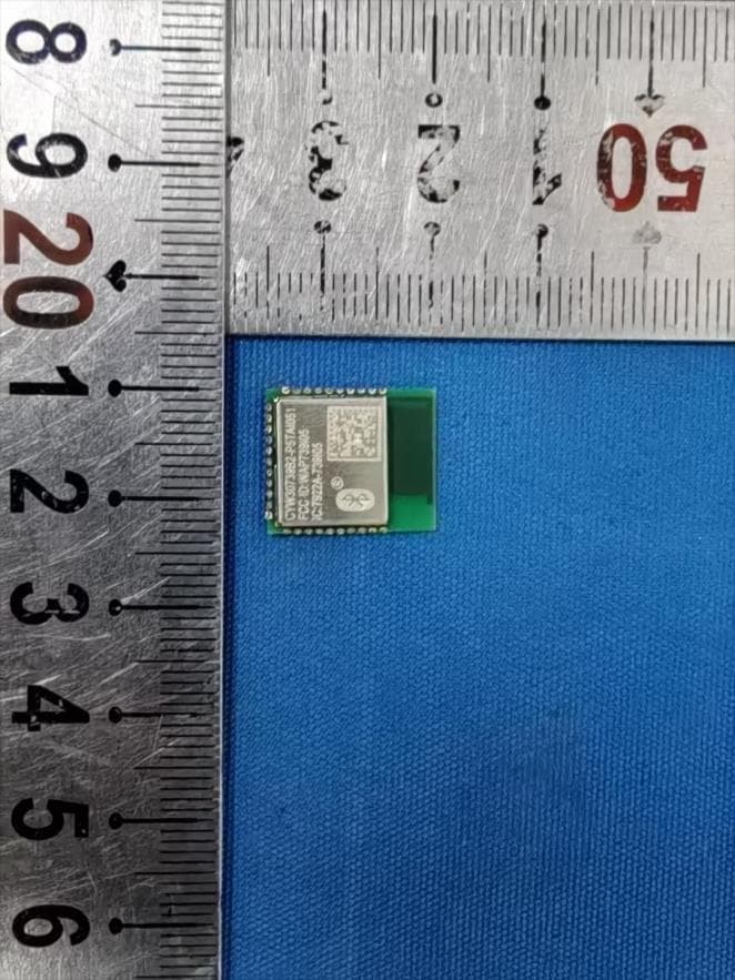
WAP739I05
Aug 01, 2024AIROC Matter Module
Equipment Class
DTS - Digital Transmission SystemWAP829I10
Jan 16, 2024AIROC Bluetooth LE Module
Equipment Class
DTS - Digital Transmission System
WAP3068
Jun 28, 2020EZ-BT WICED Module
Equipment Class
DTS - Digital Transmission System
WAP3066
Jun 23, 2020EZ-BT WICED Module
Equipment Class
DSS - Part 15 Spread Spectrum Transmitter