WS2-WG1300E00Wireless LAN EM board for Module (802.11 bg)
Jorjin Technologies Inc.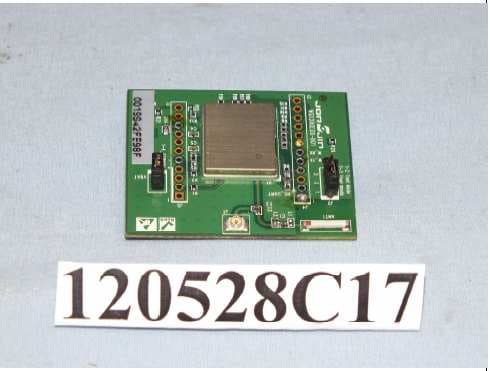
Click to zoom
Application Details
- Equipment Class
- DTS - Digital Transmission System
- Date of Grant
- Jul 09, 2012
- Application Purpose
- Original Equipment
- Date of Application
- Jul 09, 2012
- Equipment Note
- Wireless LAN EM board for Module (802.11 bg)
- Frequency Range
- 2412.00000000 - 2462.00000000
- Company
- Jorjin Technologies Inc.
- Country
- Taiwan
Documents & Files
Document Text
Text extracted from the exhibit documents filed with the FCC. Open a document above to read the original.
Users Manual
Copyright © JORJIN TECHNOLOGIES INC. 2012 http://WWW.JORJIN.COM.TW CONFIDENTIAL a module solution provider WG1300-00 EM Board User Guide Revision 0.1 Doc No: WG1300-00 EM Board-UG-D01 Copyright © JORJIN TECHNOLOGIES INC. 2012 http://WWW.JORJIN.COM.TW CONFIDENTIAL Page 1 Index 1. INTRODUCTION...........................................................................1 2. WG1300-00 EM BOARD ........................................................................................ 2 2.1. TOP SIDE ............................................................................................................. 2 2.2. BOTTOM SIDE .................................................................................................... 5 2.3. Hardware setup...........................................................................7 2.4. Schematics.................................................................................8 2.5. Bill of Material (BOM)..................................................................9 3. APPLICATION EXAMPLES............................................................10 4. HISTORY CHANGE ............................................................................................. 11 Doc No: WG1300-00 EM Board-UG-D01 Copyright © JORJIN TECHNOLOGIES INC. 2012 http://WWW.JORJIN.COM.TW CONFIDENTIAL Page 2 1. INTRODUCTION The purpose of this user guide is to help user understanding how to use WG1300-00 EM (Evaluation Module) board to complete hardware setup for test to evaluate the performances of CC3000-WG1300-00 SiP Module. 2. WG1300-00 EM BOARD In the following sub-sections, it’ll divide into TOP and BOTTOM Side to explain details on the key parts and its features. 2.1. TOP Side Figure 1 is TOP-Side picture of WG1300-00 EM Board. Figure 1. TOP Side of WG1300-00 EM Board The picture above marks some key parts and jumpers and Table 1 below shows the explanations to them in the details. J3 J2 J5 J4 J1 Antenna CC3000-WG1300-00 Module Doc No: WG1300-00 EM Board-UG-D01 Copyright © JORJIN TECHNOLOGIES INC. 2012 http://WWW.JORJIN.COM.TW CONFIDENTIAL Page 3 Items Key Parts Descriptions 1 CC3000-WG1300-00 Module The core module for performance evaluation. It’s related feature can be referred to its datasheet. 2 Antenna It can used for radiated test by reworking cpacitor to correct pads. 3 J1 It’s a U.FL RF connector via which you can proceed conducted power test. 4 J2 It is a jumper via which we can swap testing modes, test mode and operation mode. When pin 2 and pin 3 are shorted, it runs in operation mode and it operate in test mode when pin 1 and pin 2 are shorted. 5 J3 It is a jumper for testing power consumption. In operation mode, pins of the jumper is shorted. For power testing, the jumper is removed and ammeter crosses the pins to do the testing. 6 J4 Refer to Table 2. For more details on these through-hole test points 7 J5 Refer to Table 3. For more details on these through-hole test points Table 1. TOP-Side Key parts of WG1300-00 EM Board Table 2 below shows the signal descriptions of J4 Pin Number Pin Name Pin Type Descriptions 1 GND Ground 2 NS_UARTD I/O Networking subsystem UART Debug line 3 FUNC4 -- Leave floating 4 WL_UART_DBG I/O UART Debug Line 5 WL_RS232_TX O Test RS232 transmit output; Leave floating for normal operation 6 WL_RS232_RX I Test RS232 receive output; Leave floating Doc No: WG1300-00 EM Board-UG-D01 Copyright © JORJIN TECHNOLOGIES INC. 2012 http://WWW.JORJIN.COM.TW CONFIDENTIAL Page 4 for normal operation 7 GND Ground 8 WL_SPI_CS I Host interface SPI Chip Select 9 WL_SPI_DOUT O Host interface SPI Data Ouput 10 WL_SPI_IRQ O Host Interface SPI Interrupt Request 11 WL_SPI_DIN I Host Interface SPI Data Input 12 WL_SPI_CLK I Host interface SPI Clock input Table 2. TOP-Side J4 of WG1300-00 EM Board Table 3 below shows the signal descriptions of J5 Pin Number Pin Name Pin Type Descriptions 1 SCL_CC3000 O I2C Clock signal output from CC3000. This pin is connected to SCL_EEPROM via a 0-Ohm resister and is not used by end users. 2 SCL_EEPROM I I2C Clock signal input from EEPROM inside CC3000-WG1300-00 SiP Module. This pin is connected to SCL_CC3000 via a 0-Ohm resister and is not used by end users. 3 SDA_CC3000 I/O I2C Data signal from CC3000. This pin is connected to SDA_EEPROM via a 0-Ohm resister and is not used by end users. 4 SDA_EEPROM I/O I2C Data signal from EEPROM inside CC3000-WG1300-00 SiP Module. This pin is connected to SDA_CC3000 via a 0-Ohm resister and is not used by end users. 5 VBAT_SW_EN I Active-high enable signal from Host device. 6 GND Ground 7 GND Ground 8 VIO_HOST PI VIO power supply from HOST to Module. For MSP430 Host platform, VIO_HOST=VBAT_IN. For other platforms which have different voltage levels from Doc No: WG1300-00 EM Board-UG-D01 Copyright © JORJIN TECHNOLOGIES INC. 2012 http://WWW.JORJIN.COM.TW CONFIDENTIAL Page 5 Battery voltages’, R14 can be remove to support such a case. 9 VBAT_IN PI Battery voltage input to Module. For MSP430 Host platform, VIO_HOST=VBAT_IN. For other platforms which have different voltage levels from Battery voltages’, R14 can be remove to support such a case. 10 GND Ground 11 EXT_32KHz I External Slow Clock input from Host device. It can be used for the SiP Module inside which hasn’t slow clock source. Table 3. TOP-Side J5 of WG1300-00 EM Board 2.2. BOTTOM Side Figure 2 is BOTTOM-Side picture of WG1300-00 EM Board. Figure 2. Bottom Side of WG1300-00 EM Board There are two EM Board mating connectors which are used for connecting to Host platform and are mounted on the bottom side as the picture above. Table 4 and Table 5 show the descriptions on the J6 J7 Doc No: WG1300-00 EM Board-UG-D01 Copyright © JORJIN TECHNOLOGIES INC. 2012 http://WWW.JORJIN.COM.TW CONFIDENTIAL Page 6 signals brought out from these two EM mating connectors. J6 Pin Number Pin Name Module Pin Type Description 1 GND Ground 5 EXT_32KHz I External Slow Clock input from Host device. It can be used for the SiP Module inside which hasn’t slo…
Text truncated - open the document above for the full version.
Users Manual
Federal Communication Commission Interference Statement This device complies with Part 15 of the FCC Rules. Operation is subject to the following two conditions: (1) This device may not cause harmful interference, and (2) this device must accept any interference received, including interference that may cause undesired operation. This equipment has been tested and found to comply with the limits for a Class B digital device, pursuant to Part 15 of the FCC Rules. These limits are designed to provide reasonable protection against harmful interference in a residential installation. This equipment generates, uses and can radiate radio frequency energy and, if not installed and used in accordance with the instructions, may cause harmful interference to radio communications. However, there is no guarantee that interference will not occur in a particular installation. If this equipment does cause harmful interference to radio or television reception, which can be determined by turning the equipment off and on, the user is encouraged to try to correct the interference by one of the following measures: - Reorient or relocate the receiving antenna. - Increase the separation between the equipment and receiver. - Connect the equipment into an outlet on a circuit different from that to which the receiver is connected. - Consult the dealer or an experienced radio/TV technician for help. FCC Caution: Any changes or modifications not expressly approved by the party responsible for compliance could void the user's authority to operate this equipment. This transmitter must not be co-located or operating in conjunction with any other antenna or transmitter. Radiation Exposure Statement: This equipment complies with FCC radiation exposure limits set forth for an uncontrolled environment. This equipment should be installed and operated with minimum distance 20cm between the radiator & your body. This device is intended only for OEM integrators under the following conditions: 1) The antenna must be installed such that 20 cm is maintained between the antenna and users, and 2) The transmitter module may not be co-located with any other transmitter or antenna. As long as 2 conditions above are met, further transmitter test will not be required. However, the OEM integrator is still responsible for testing their end-product for any additional compliance requirements required with this module installed IMPORTANT NOTE: In the event that these conditions can not be met (for example certain laptop configurations or co-location with another transmitter), then the FCC authorization is no longer considered valid and the FCC ID can not be used on the final product. In these circumstances, the OEM integrator will be responsible for re-evaluating the end product (including the transmitter) and obtaining a separate FCC authorization. End Product Labeling This transmitter module is authorized only for use in device where the antenna may be installed such that 20 cm may be maintained between the antenna and users. The final end product must be labeled in a visible area with the following: “Contains FCC ID: WS2-WG1300E00”. The grantee's FCC ID can be used only when all FCC compliance requirements are met. Manual Information To the End User The OEM integrator has to be aware not to provide information to the end user regarding how to install or remove this RF module in the user’s manual of the end product which integrates this module. The end user manual shall include all required regulatory information/warning as show in this manual.
Cover Letter(s)
FCC ID: WS2-WG1300E00 Report No.: RF 120528C17 Modular Approval Request Letter Bureau Veritas Consumer Products Services (H.K.) Ltd., Taoyuan Branch July 6, 2012 Dear Application Examiner, JORJIN TECHNOLOGIES INC., It’s a Wireless LAN EM board for Module (802.11 bg), FCC ID: WS2-WG1300E00 would like to have your authorization as a modular approval specific to the mobile RF exposure condition. The requirements of section 15.212 of FCC rules have been met and shown on the following statements. 1. “The modular transmitter must have its own RF shielding.” The radio portion of this module has been shielded, please see exhibition External Photo. 2. “The modular transmitter must have buffered modulation/data inputs.” The EUT has buffered data inputs, it is integrated in chip CC3000. 3. “The modular transmitter must have its own power supply regulation.” The part number of this regulator is TPS79718 4. “The modular transmitter must comply with the antenna requirements of section 15.203 and 15.204(C).” The EUT meets the FCC antenna requirements. The spurious emission, unique antenna connector and photo of antennas are shown in the test report. 5. “The modular transmitter must be tested in a stand-alone configuration” The EUT was tested in a stand-alone configuration via a extender. Please see section Photographs of Test Configuration in the test report, the EUT was plugged in this extender. 6. “The modular transmitter must be labeled with its own FCC ID number.” Please see exhibition Label Sample for the FCC ID of this module. And also in the exhibition Users Manual, there are instructions give to the OEM on how to label the end product. FCC ID: WS2-WG1300E00 Report No.: RF 120528C17 7. “The modular transmitter must comply with any specific rule or operating requirements applicable to the transmitter and the manufacturer must provide adequate instructions along with the module to explain any such requirements.” The EUT is compliant with all applicable FCC rules. Detail instructions for maintaining compliance are given in the Users Manual. 8. “The modular transmitter must comply with any applicable RF exposure requirements.” The EUT is compliant with all applicable RF exposure requirements. RF Exposure is addressed in the RF exposure exhibition. Please contact me if you have any further questions. Thanks for your attention. Best Regards, signature Gary Chang Technical Manager Bureau Veritas Consumer Products Services (H.K.) Ltd., Taoyuan Branch
ID Label/Location Info
Model No:WG1300E00 FCC ID: WS2-WG1300E00 IC: 10462A-J1300E00 27mm 15mm
Internal Photos
Page 2 Page 3
Operational Description
FCC ID: WS2-WG1300E00 Report No.: RF 120528C17 Operational Description This device is a Wireless LAN EM board for Module (802.11 bg), which operates in 2.4GHz band; the maximum data rate could be up to 54Mbps which OFDM technique. If the signal to noise radio is too poor which could not support 54Mbps, the 11Mbps data rate with DSSS technique will be applied. The transmitter of the EUT is powered by the 3.3Vdc from host equipment. The antennas is chip antenna. The other instruction, please have a look at the users manual.
RF Exposure Info
Report No.: SA120528C17 1 of 5 Report Format Version 5.0.0 RF EXPOSURE REPORT REPORT NO.: SA120528C17 MODEL NO.: WG1300E00 FCC ID: WS2-WG1300E00 RECEIVED: May 28, 2012 TESTED: May 31 ~ Jun. 05, 2012 ISSUED: Jun. 13, 2012 APPLICANT: JORJIN TECHNOLOGIES INC. ADDRESS: 5F., No. 28, Lane 141, Sing-ai Rd., Neihu District, Taipei City 114, Taiwan ISSUED BY: Bureau Veritas Consumer Products Services (H.K.) Ltd., Taoyuan Branch LAB ADDRESS: No. 47, 14th Ling, Chia Pau Vil., Lin Kou Dist., New Taipei City, Taiwan ( R.O.C. ) TEST LOCATION: No. 19, Hwa Ya 2nd Rd, Wen Hwa Tsuen, Kwei Shan Hsiang, Taoyuan Hsien 333, Taiwan, R.O.C. This report is for your exclusive use. Any copying or replication of this report to or for any other person or entity, or use of our name or trademark, is permitted only with our prior written permission. This report sets forth our findings solely with respect to the test samples identified herein. The results set forth in this report are not indicative or representative of the quality or characteristics of the lot from which a test sample was taken or any similar or identical product unless specifically and expressly noted. Our report includes all of the tests requested by you and the results thereof based upon the information that you provided to us. You have 60 days from date of issuance of this report to notify us of any material error or omission caused by our negligence, provided, however, that such notice shall be in writing and shall specifically address the issue you wish to raise. A failure to raise such issue within the prescribed time shall constitute your unqualified acceptance of the completeness of this report, the tests conducted and the correctness of the report contents. Unless specific mention, the uncertainty of measurement has been explicitly taken into account to declare the compliance or non-compliance to the specification. Report No.: SA120528C17 2 of 5 Report Format Version 5.0.0 TABLE OF CONTENTS RELEASE CONTROL RECORD ................................................................................................ 3 1. CERTIFICATION ............................................................................................................. 4 2. RF EXPOSURE ............................................................................................................... 5 2.1 LIMITS FOR MAXIMUM PERMISSIBLE EXPOSURE (MPE) ......................................... 5 2.2 MPE CALCULATION FORMULA .................................................................................... 5 2.3 CLASSIFICATION ........................................................................................................... 5 2.4 CALCULATION RESULT OF MAXIMUM CONDUCTED POWER .................................. 5 Report No.: SA120528C17 3 of 5 Report Format Version 5.0.0 RELEASE CONTROL RECORD ISSUE NO. REASON FOR CHANGE DATE ISSUED SA120528C17 Original release Jun. 13, 2012 Report No.: SA120528C17 4 of 5 Report Format Version 5.0.0 1. CERTIFICATION PRODUCT: Wireless LAN EM board for Module (802.11 bg) MODEL: WG1300E00 BRAND: Jorjin APPLICANT: JORJIN TECHNOLOGIES INC. TESTED: May 31 ~ Jun. 05, 2012 TEST SAMPLE: ENGINEERING SAMPLE STANDARDS: FCC Part 2 (Section 2.1091) FCC OET Bulletin 65, Supplement C (01-01) IEEE C95.1 The above equipment (Model: WG1300E00) has been tested by Bureau Veritas Consumer Products Services (H.K.) Ltd., Taoyuan Branch, and found compliance with the requirement of the above standards. The test record, data evaluation & Equipment Under Test (EUT) configurations represented herein are true and accurate accounts of the measurements of the sample’s EMC characteristics under the conditions specified in this report. PREPARED BY : , DATE:Jun. 13, 2012 Pettie Chen / Specialist APPROVED BY : , DATE:Jun. 13, 2012 Gary Chang / Technical Manager Report No.: SA120528C17 5 of 5 Report Format Version 5.0.0 2. RF EXPOSURE 2.1 LIMITS FOR MAXIMUM PERMISSIBLE EXPOSURE (MPE) FREQUENCY RANGE (MHz) ELECTRIC FIELD STRENGTH (V/m) MAGNETIC FIELD STRENGTH (A/m) POWER DENSITY (mW/cm 2 ) AVERAGE TIME (minutes) LIMITS FOR GENERAL POPULATION / UNCONTROLLED EXPOSURE 300-1500 ... ... F/1500 30 1500-100,000 ... ... 1.0 30 F = Frequency in MHz 2.2 MPE CALCULATION FORMULA Pd = (Pout*G) / (4*pi*r 2 ) where Pd = power density in mW/cm 2 Pout = output power to antenna in mW G = gain of antenna in linear scale Pi = 3.1416 R = distance between observation point and center of the radiator in cm 2.3 CLASSIFICATION The antenna of this product, under normal use condition, is at least 20cm away from the body of the user. So, this device is classified as Mobile Device. 2.4 CALCULATION RESULT OF MAXIMUM CONDUCTED POWER Frequency BAND (MHz) Max power (dBm) Antenna gain (dBi) Distance (cm) Power Density (mW/cm 2 ) Limit (mW/cm 2 ) 2412-2462 23.12 2.5 20 0.073 1
Test Setup Photos
1 PHOTOGRAPHS OF THE TEST CONFIGURATION CONDUCTED EMISSION TEST 2 3 RADIATED EMISSION TEST 4
Contact Information
Applicant
Alan Lin(Engineering Vice President)
Technical Contact
Bureau Veritas CPS (H.K.) Ltd. Taoyuan BranchGary Chang
[email protected]886-3-3183232
No. 19, Hwa Ya 2nd Rd., Kwei Shan Hsiang · Taoyuan Hsien · Taiwan
Non-Technical Contact
Bureau Veritas CPS (H.K.) Ltd. Taoyuan BranchCeline Chou
[email protected]886-3-3183232
Test Firm
Bureau Veritas CPS (H.K.) Ltd. Taoyuan BranchRichard Chen
Technical Specifications
| # | Rule Parts | Frequency Range | Power Output |
|---|---|---|---|
| 1 | 15C | 2.41 GHz - 2.46 GHz | 205.00 mW |
Other Applications from Jorjin Technologies Inc.
WS2-MT5C0103A
Jul 24, 2026Radar Product
Equipment Class
FDS - Part 15 Field Disturbance Sensor
WS2-WB2072-00
May 02, 2021Bluetooth Module
Equipment Class
DTS - Digital Transmission System
WS2-WG3221B
Apr 28, 2020WiFi and Bluetooth module
Equipment Class
DSS - Part 15 Spread Spectrum Transmitter
WS2-WG1400-00
Nov 26, 2015Wireless module
Equipment Class
DTS - Digital Transmission System
WS2-WG7833B0
Aug 27, 2015Wireless Module
Equipment Class
DSS - Part 15 Spread Spectrum Transmitter